
Abstract
Power modules in electric vehicles (EVs) are essential electronic components that manage and convert electrical power between the battery and other vehicle systems, such as the motor. The electronics are required to operate at higher temperatures (>200 oC) and fields (>0.5 MV/cm) than in conventional consumer goods such as phones and tablets. This requires the use of, e.g., SiC based semiconductor technology, along with associated filters/capacitors that can withstand high temperature/fields. Such capacitors have a large energy density arising from the ability of the dielectric to withstand repeated application of high fields (>0.5 MV/cm) without breakdown. This article reviews examples and presents new data and concepts on high energy density dielectrics intended for use in power electronic. In particular, the article focuses on a new class of dielectrics which have high permittivity (>1000) but do not saturate at high field and exhibit a quasi-linear polarisation-field response. The roles of chemical, polar and octahedral tilt disorder are assessed and a new mechanism proposed by which tilt disorder restricts strain coupling and therefore polar coupling, leading to a quasi-linear response in polarisation-field (P-E) loops. The influences of local variations in stoichiometry and multi-valent and multi-sized substituents in these polar lattices to attain enhanced resistivity are also discussed. The article therefore illustrates how a combination of high resistivity and tilt disorder are pivotal in the design of a new generation of high energy density capacitors for power electronics.
Introduction
Power electronics will play a central role in the impending energy transition from fossil fuels to electrification, which will profoundly change transport and energy distribution infrastructure. New wide-bandgap semiconductor technologies provide active components that can operate at 200 °C or above, allowing reductions in heatsink size and equipment weight. 1 However, the high switching speeds of these wide-bandgap devices require that passive and active components must be in close proximity (i.e., co-packaged), demanding high temperature operation of the passive components. The development of next generation Class-II dielectrics with a wide operating temperature range, from −55 to 200–300 °C (operating window for power electronics), is thus of global importance. In addition, they must work at higher operating fields (>500 kV/cm), be Pb-free and not prohibitively expensive to manufacture, i.e., compatible with base metal electrodes (BME) such as Ni.
Over the last decade many attempts have been made to replace BaTiO3, the dominant dielectric in the manufacture of multilayer ceramic capacitors (MLCCs) in consumer electronics, for one better suited to power electronics. The breakdown strength and operating temperature of classic X7R BaTiO3-based dielectrics are too low and the dielectric ‘tunes’ at high field, limiting the permittivity to ∼300 rather than 2000 at low field. To date, high permittivity compositions such as Bi-based relaxors (REL) 2 and various anti-ferroelectric (AFE) 3 compositions have been proposed but they are either incompatible with low-cost electrodes (Bi reacts with Ag-0.1Pd and Ni) and/or exhibit large strains leading to mechanical failure due to either a field induced transition from AFE to FE or REL to FE. As a result, the default mode in power electronics is currently CaZrO3 based dielectrics whose volumetric efficiency is low due to their low permittivity (εr ∼30). 4
Much emphasis in the field of high voltage capacitors has been placed on recovery/discharge energy density (Wrec, given by the area to the left of a unipolar P-E curve (shaded areas in Figure 1).2,3 Wrec is an excellent ‘Figure of Merit’ to compare materials for power electronic applications, particularly if the P-E loops are obtained as a function of temperature since high maximum electric field (Emax) necessitates high breakdown strength and dP/dE = ε.2,3 Figure 1(a) illustrates a FE response in which dP/dE = 0 at high field (tunes). Figure 1(b) is from a relaxor (REL) in which dP/dE → 0, i.e., the dielectric still tunes and permittivity reduces at high field but not to the extent of FE materials. Figure 1(c) is an example of a linear (or quasi-linear) dielectric (QLD) in which dP/dE is effectively constant (k) and does not tune. QLDs differ from conventional linear dielectrics in that they have considerably higher εr (>600) as opposed to 10 for alumina 5 or 30 for CaZrO3. 4 Such large values of εr with virtually linear P-E response is until recently unknown. We propose therefore that an ideal dielectric for high field applications should not tune (dP/dE = k), have a high εr (>500) and should not significantly deviate from its room temperature characteristics above 200 oC (temperature stable). The area enclosed by the P-E loops in Figure 1 approximates to high field loss (Wloss) and gives the efficiency (η) of the dielectric during discharge as Wrec/(Wrec + Wloss). Opening of the loop, relates to the switching of domains and/or the movement of defects (i.e., ionic and/or electronic conduction) under the applied field. Both are a source of dielectric loss in the system and can lead to self-heating of the MLCC. η therefore is an ideal ‘Figure of Merit’ to assess the high field loss and should be close to 100% for MLCCs for power electronics. 2
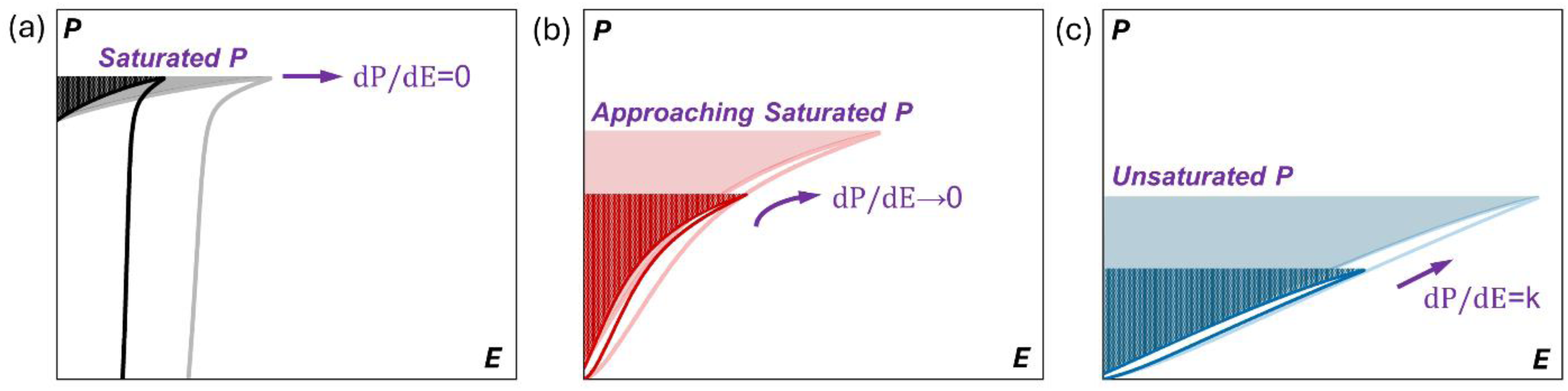
Schematic of unipolar P-E loops of different dielectrics for electrostatic energy storage: a) ferroelectric (dP/dE = 0); b) relaxor ferroelectric (dP/dE → 0) and c) quasi-linear dielectrics (dP/dE = constant, k).
There are a number of AFE systems, mainly based on NaNbO3 (NN) and AgNbO3 (AN) which have been explored for pulsed power application. 3 They have a high energy density but for high voltage capacitors a sudden step change in permittivity at the field induced transition, prohibits their use in power electronics. Instead, relaxor or paraelectric systems are preferred in which the change in εr as a function of field and temperature is more predictable.6–12 Empirically, the importance of chemical disorder in the development of high voltage dielectric relaxor-ferroelectric and paraelectric ceramics is well established.6–12 Many authors now choose to express perovskite compositions using a single ABO3 formula, i.e., with multiple A- and B-site ions, rather than as ternary or quaternary solid solutions, thereby emphasising the ‘high entropy’ within the composition.13,14 High entropy oxides consist of five or more metallic elements in near-equimolar proportions, forming a single-phase solid solution. The high configurational entropy is said to stabilise these materials in either non-equilibrium crystal structures and/or imparts them with novel properties. 15 There is no strong evidence of stabilisation of non-equilibrium structures within high voltage/energy dielectrics since all materials form conventional solid solutions.16,17 In some cases however, end members are introduced into the solid solution which do not in themselves form a stable perovskite structure, such as BiMg2/3Nb1/3O3 in BaTiO3 – BiFeO3 – BiMg2/3Nb1/3O3.18,19 Whilst it can be argued that BiMg2/3Nb1/3O3 is ‘entropy stabilised’, equally Mg2+ and Nb5+ may be viewed as entering into solid solution as ionically compensated dopants, an effect that has been known for number of years. More fundamentally, considerations of entropy constitute a phenomenological approach dealing with macroscopic properties which by definition do not engender a microscopic or mechanistic understanding. It should also be noted that the materials described in ref Wang et al. 20 are composed of ∼80% NN and do not conform to any definition commonly used for high entropy dielectrics yet exhibit some of the highest values of Wrec reported to date for MLCCs.
Nonetheless, it is evident that increasing the number of different A- and B-site species within systems that contain highly polarisable cations such as Bi, Nb, Ti and Pb reduces polar order, forcing a relaxor or paraelectric state.6–12 The distribution of valence states/ion-size throughout the A and B-sites contributes to a high breakdown strength, despite no macroscopic driving force for the formation of defects since they are substituted into the lattice with the appropriate ionic compensation, i.e., they are stoichiometric substituents.6–12 However, non-stoichiometric defects may form locally which are compensated over larger volumes, creating a short range ordered multi-defect state that appears critical for optimising breakdown strength and by default energy density. In this article, we will describe examples of the stoichiometric alloying effect and postulate about the possible mechanisms by which resistivity is enhanced.
Almost all papers, consider chemical and polar disorder as factors that contribute to the design of high voltage/energy density dielectric ceramics.6–12 Only a few in contrast, consider the role of distortions of the BO3 octahedral framework, despite the largest energy densities and break down strengths in perovskite structured dielectrics being associated with octahedral tilted or short range tilted systems.20,21 Moreover, the recent demonstration of large energy densities in a tetragonal tungsten bronze (TTB) structured ferroics whose octahedral tilt structure forms a frustrated incommensurate lattice, 22 reinforces the view that octahedral tilt disorder is pivotal in designing ceramics for high voltage/energy density applications.
Role of doping/alloying in the control of electrical properties
A) Intrinsic resistivity and breakdown strength
The two main factors that influence insulation resistance (IR) and breakdown strength (BDS) are the (physical) ceramic and electrical microstructure of the dielectric body, which may or may not be the same. The physical microstructure can contain many different features, for example, a distribution of grain sizes and shapes and level/shape/distribution of porosity, inter-grain boundary regions of different thickness and/or composition, intra-grain regions based on core and shell regions and/or surface layers on the ‘skin’ of the ceramics with different composition and/or distribution of defects such as oxygen vacancies. Each of these regions (if present) can have their own electrical properties (e.g., values of permittivity and conductivity) and depending on their relative values can influence the measured electrical properties. The electrical microstructure is based on how the current is transported through these various electro-active regions (for IR) and how the electric field is supported within the ceramic (for BDS).
In general, most researchers use only low field measurements to assess IR of ceramics via methods such as Impedance Spectroscopy (IS), where a low ac signal, typically 100 mV across a wide frequency range (e.g., 10−2 to 106 Hz) is applied across a sample that is 1–2 mm thick with symmetric (top and bottom) electrodes. 23 In contrast BDS on the same samples is often estimated from P-E measurements where much higher ac fields, e.g., > 300 kV/cm are applied at a selected frequency, e.g., 1 Hz. 2 These are very different measurements and provide different but complimentary information on the electrical microstructure and properties, notwithstanding that the electrical properties of many of these regions may exhibit non-ohmic (i.e., voltage dependent) behaviour. Furthermore, to test ceramics at higher fields and avoid arcing (or air breakdown) around the sample, it has become common practice in P-E measurements to employ a smaller-area top electrode paired with a full bottom electrode. 24 For small top-electrode areas, this configuration can generate significant non-uniformity and extremely high electric fields, along with spreading resistance effects near the top contact. Such issues distort P-E loop shapes (and thus the extracted values for Wrec, Wloss and η), as well as BDS estimates. 24 For example, in BaTiO3 ceramics, increasing the thickness-to-top-electrode radius ratio (S/r) from 0.17 to 1.96 broadens and distorts loops, raising Wrec by approximately 1.4 times and drops η from 29 to 8%. These effects arise from geometric confinement and electrode interference, leading to underestimation of the local field at high S/r values. To promote reproducibility and fair comparisons, researchers should report electrode areas, sample thicknesses, and S/r ratios alongside P-E data. Although no universal standard exists, it is advisable to use top and bottom electrodes of equal area (covering > 80% of the sample surface) for bulk ceramics, thereby minimising field non-uniformity and approximating full top-bottom configurations. Equally important is correcting for thickness effects; thus, good metrology demands disclosure of both electrode areas and sample thickness in P-E studies. Normalisation offers an effective way to mitigate thickness- and area-related biases. Thinner samples (< 0.2 mm) can boost Emax up to fourfold through defect reduction, while smaller areas (< 1 cm2) roughly double ΔP (and hence Wrec), as reported by Wang et al. 25 It is recommended to normalise energy-storage performance using thickness-independent metrics such as Wn = Wrec/Emax and area-independent ones such as Wn = Wrec/ΔP, enabling cross-format comparisons across bulk, multilayer, and thin-film systems.
In the case of IS, it is often possible to assess (at least at low electric fields) the IR electrical properties of different electro-active regions, whereas for P-E measurements this is not possible as the area within the loops contains contributions from dipoles through domain switching, and conduction though e.g., the migration of oxygen vacancies with samples.
The brickwork layer model (BLM) is often used to analyse IS data of electroceramics and works well when the grain boundary regions are more resistive than the grains (bulk), i.e Rgb >> Rb, levels of porosity are low (< 5 vol%) and there is a uniform grain structure. 22 In this model, the current pathway is assumed to be a simple series connection of these electroactive regions and the total (IR) resistance is Rb + Rgb. Thus, to maximise IR, it is advantageous to have small grains to ensure a high-volume fraction of grain boundaries and to minimise porosity to avoid arcing within the ceramic that can lead to low BDS during P-E measurements. If the grains contain a core-shell microstructure, then providing Rshell >> Rcore the BLM is still applicable and the total resistance of the ceramic is Rcore + Rshell + Rgb.23,26 The electrical homogeneity of the grains is best probed by analysing the complex electric modulus formalism (M*) which is sensitive to small (and therefore bulk-type) capacitances. The total resistance of the ceramics is best analysed by the complex impedance formalism (Z*) which is dominated by the most resistive regions which is typically the grain boundaries, if they are electro-active. Combined -Z″ and M″ spectra are therefore often a convenient way to present IS data to visually assess the electrical homogeneity of electroceramics.23,26
B) Defect chemistry in ferroics
Most ferroic perovskite and TTB materials are based on B-site do cations, i.e., BaTiO3, Pb(Zr,Ti)O3, NaNbO3, (Na1/2Bi1/2)TiO3 and (Ba,Sr)Nb2O6. They exhibit wide band gaps (> 3 eV) and are therefore a natural choice as dielectric materials since their intrinsic conductivity (i.e., conduction across the band gap between a filled valence band and empty conduction band) should remain low until high temperatures. One exception is BiFeO3 which is based on Fe3+ (d5) with a band gap of 2.8 eV but this remains sufficient to adequately assess the dielectric behaviour. Due to their low levels of intrinsic conduction near room temperature (RT), the leakage conduction mechanism(s) are either predominantly extrinsic due to aliovalent impurities (i.e., donors or acceptors) and/or due to non-stoichiometry associated with a significant deviation from A/B = 1 in nominally stoichiometric ABO3 perovskites. This A/B non-stoichiometry may exist intrinsically in the material and/or be induced by ceramic processing. Examples are given below to illustrate how unintentional impurities (BaTiO3), small variations in A/B ratios ((Na1/2Bi1/2)TiO3) and loss of Bi2O3 (BiFeO3) during processing can dominate the conduction properties in single perovskites, precursor to considering the binary/ternary/quaternary systems in high energy density applications.

Electrons are required to form the O2− ions and therefore holes are created in the valence band (or as O− as opposed to O2− ions in the lattice 28 ) and low levels of p-type conduction arise. The residual oxygen vacancies are not the predominant source of conduction under low electric fields but are a source of oxide-ion (ionic) conduction under high electric fields where ion migration can be appreciable. 29 For high field dielectric applications, the presence of oxygen vacancies are detrimental to material performance and their concentration should be minimised.
(
Low levels of A-site non-stoichiometry can be induced by changing the Na/Bi ratio in the nominal starting composition and/or by volatilisation of Bi2O3 during ceramic processing of nominally stoichiometric NBT.30,32 The level of Bi2O3 volatilisation is influenced by the polymorphic form of the TiO2 reagent (anatase or rutile) used in the solid-state reaction method. The former is more effective in suppressing Bi2O3 loss by forming sillenite Bi12TiO20 prior to forming perovskite NBT.
34
In this way, nominally stoichiometric NBT prepared using anatase is an excellent dielectric which remains electrically insulating with bulk conductivity, σ ∼ 2 mS/cm (at 600 oC) with an activation energy for bulk conduction of 1.7 eV (approximately half the band gap). In contrast, significant Bi2O3 loss occurs when using rutile as there is no formation of Bi-rich precursor phase(s) at lower temperature prior to perovskite NBT and this generates A-site and oxygen vacancies during ceramic processing according to the following equation

This gives rise to bulk (grain) oxide-ion conductivity that is 3 orders of magnitude higher at 600 oC with an activation energy of < 0.5 eV. 34 This is another example of the important influence that starting reagents (structure and purity) can have in controlling the resulting electrical properties of the target material. It also demonstrates how challenging it can be to achieve the desired electrical properties in ceramics prepared by solid state reactions when low levels (commonly < 1 at%) of impurities and/or non-stoichiometry can have such dramatic effects.
Studies (using rutile TiO2) have confirmed the Na/Bi starting ratio plays a significant role in the electrical properties and to be a reliable method to ensure either dielectric or oxide-ion (electrolyte) behaviour in NBT. Nominal non-stoichiometry was induced by preparing both Bi- and Na-excess/deficient NBT materials, viz Na1/2Bi1/2 + xTiO3 + 1.5−x/2 (x = -0.01, NB0.49 and +0.01, NB0.51) and Na1/2 + yBi1/2TiO3 + 0.50y (y = -0.01, N0.49B and +0.01, N0.51B), respectively. In cases where Na/Bi < 1 (NB0.51 and N0.49B) dielectric behaviour was observed, whereas for Na/Bi > 1 (NB0.49 and N0.51B) electrolyte behaviour was obtained, Figure 2(a). 34 Full explanations of these different types of un-doped behaviour can be found elsewhere 29 ; however, it is important to appreciate that oxide-ion conduction in NBT (and other perovskites) occurs by a hopping mechanism via a saddle point (or bottle neck) between two A-site cations and a B-site cation.
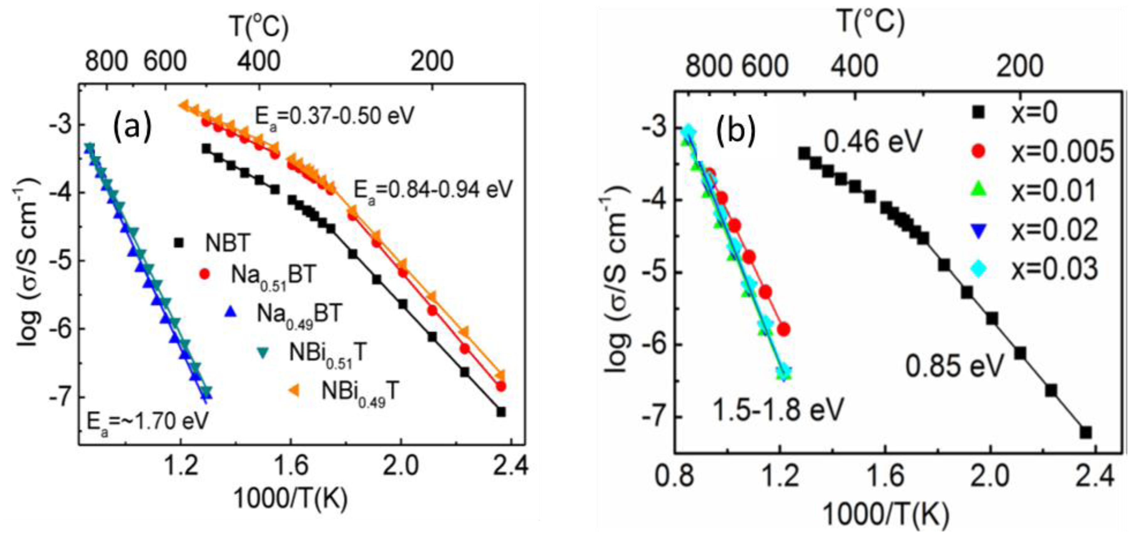
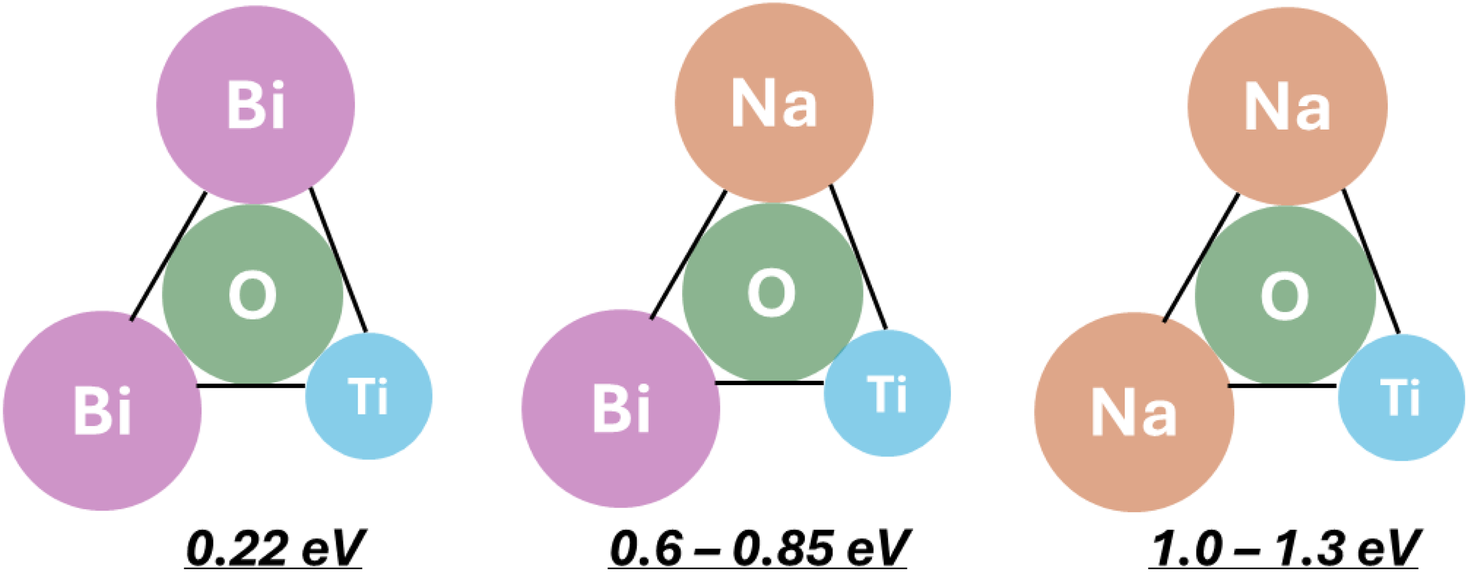
The activation energy, Ea for the oxide ion conduction in NBT (where the Na and Bi ions are disordered on the A-sites) is extremely sensitive to the local bonding of oxygen with the surrounding cations and has been calculated to vary from ∼ 0.22 eV where both A-site ions are Bi ions to > 1.0 eV when both are Na ions, Figure 3.
33
The experimental Ea values are closer to the intermediate case of mixed Na/Bi occupation which is in broad agreement with average (disordered A site) crystal structure. This example, where Bi and Na are nominally the same size yet large differences in Ea occur, illustrates that simple crystallochemical considerations such as size (and therefore) strain may not always explain variations in oxide ion conductivity in perovskites.36,37 In the case of NBT, other considerations such as the weaker bond strength of Bi to O compared to Na and its higher polarizability are important factors. The local arrangement of the A and B site cations in perovskites and their influence on any oxide-ion conductivity is therefore a combination of multiple contributing factors. ‘Classic’ acceptor and donor doping strategies can be used to enhance or suppress the oxide-ion conductivity in undoped NBT. In these cases, ionic compensation (as opposed to electronic defects) is more favourable and several options are available.
32
For example, either A or B-site acceptor doping with low levels of Sr2+ for Bi3+ and Mg2+ for Ti4+, respectively can increase the level of oxygen vacancies via the following equations and enhance the oxide ion conductivity


In contrast donor doping with Nb5+ for Ti4+ can be effective in filling oxygen vacancies and switch oxide-ion conducting undoped NBT into an excellent dielectric material, Figure 2(b).
38

Thus far, only single dopants have been considered where the choice of appropriate aliovalent dopants is well established as an effective way to optimise the electrical performance. This minimises IR and therefore promotes the higher BDS required for high energy density applications. However, most materials that are being developed are not based on single materials but are solid solutions of binary/ternary/quaternary systems based on various nominally stoichiometric perovskites. These are commonly a combination of I-V, II-IV and III-III-type ABO3, e.g., NaNbO3-SrTiO3-La(Mg1/2Ti1/2)O3. Although nominally stoichiometric, local variations in stoichiometry may occur (due to A/B ≠1) and properties vary/fluctuate (due to donor- and/or acceptor-rich regions) on a submicron level. Achieving chemical (and therefore electrical) homogeneity in such multi-cation-rich perovskites is not trivial given the different diffusion kinetics (and volatility) of the various cations involved and their ability to act as possible donor and/or acceptor dopants.
A simple but illustrative example is that of nominally compensated, acceptor-donor doping of TiO2 by couples such as In3+-Nb5+ and Ga3+-Nb5+ at low dopant levels, i.e., [(Ga or In)1/2Nb1/2]xTi1−xO2 with x ≤ 0.10. These materials attracted attention as apparent colossal permittivity materials with temperature- and frequency-independent permittivity > 104 and dielectric loss < 0.1 from ∼ 50 to 450 K. This behaviour was initially attributed to electron-pinned defect dipoles at low dopant concentrations 40 however, subsequent studies demonstrated a much simpler explanation associated with electrical heterogeneity in the material due to the challenges associated with controlling the precise acceptor-donor stoichiometry at these low (< 10 at%) doping levels during the growth of single crystals 41 and ceramic processing. 42 Due to the higher volatility of Ga and In acceptor dopants, low levels of non-stoichiometry in the Nb-acceptor couple develop due to loss of Ga and In and the excess donors are electronically compensated by partial reduction of Ti4+ (do) to Ti3 + (d1) which induces n-type (electronic) semiconductivity in the grains. The grain boundaries and /or surface layers in the ceramics are electrically more resistive and this results in the development of Schottky barriers at grain boundaries and/or surface layer-electrode (non-ohmic) contacts. These mechanisms and apparent colossal permittivity are similar to that reported in CaCu3Ti4O12.43–45
From an electrical perspective it is important that electrical homogeneity is obtained to ensure high IR (or low conductivity) and BDS is obtained in these multicomponent perovskites and TTBs. IS can be a useful probe, at least on a micron level, to ensure the electrical microstructure is sufficiently homogeneous in such ceramics without knowing the precise distributions of the various cations. We illustrate this via three examples.
C) Worked examples of doping/alloying to enhance resistivity
0.6BiFeO3-0.4SrTiO3-xNb where x = 0.00, 0.01, 0.03 6
The first example is the influence of Nb2O5 additions on 0.6BiFeO3-0.4SrTiO3 ceramics. Without any addition of Nb2O5, the ceramics are leaky semiconductors due to the issues discussed above for BiFeO3, and a measurable IS response can be obtained from room temperature, RT. Based on Z* plots, x = 0.00 ceramics have a total resistivity of ∼ 180 kΩcm at RT, Figure 4(a). The corresponding combined -Z″ and M″ spectroscopic plots both display two broad and overlapping peaks with the largest peaks in the -Z″ and M″ peaks separated by ∼ 2 orders of magnitude on a log frequency scale, Figure 4(b). This indicates at least two electroactive components and therefore electrical heterogeneity in x = 0.00 ceramics. In contrast, x = 0.01 and 0.03 are electrically insulating at RT and useful IS data can only be obtained > 400 oC. Z* plots at 430 oC show a single arc with total resistivity of ∼ 40 to 60 kΩcm, Figure 4(a) and the corresponding combined -Z″, M″ spectra (of x = 0.01 Nb addition) to contain a single, near-ideal Debye peak that overlap on a log f scale, Figure 4(c). This indicates a single electroactive response and is consistent with a homogeneous electrical microstructure. In most circumstances, the largest M″ peak corresponds to a bulk (grain) dominated response and an Arrhenius plot of conductivity based on this analysis for all these ceramics is shown in Figure 4(d). There is a dramatic change in both the magnitude and activation energy of the bulk conductivity with the addition of Nb2O5. It changes from being ∼ 5.5 μS/cm at RT for x = 0.00 to ∼ 1 μS/cm at 350 oC with an increase in Ea from ∼ 0.4 to 1.2 eV. This is consistent with a switch from p-type semiconductivity associated with mixed Fe3+/Fe4+ in x = 0.00 towards something that is closer to intrinsic-type conduction which is beneficial for both IR and BDS.
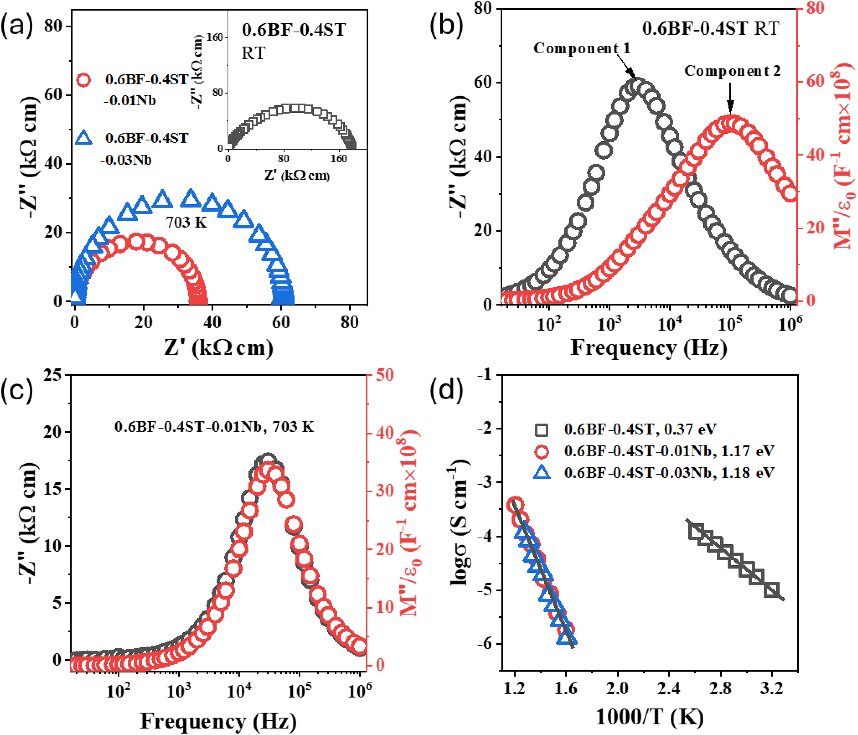
Z* plots, -Z″, M″ spectra and Arrhenius plots of bulk conductivity for various 0.6BF-0.4ST ceramics with and without additions of Nb2O5. Z* plot for 0.6BF-0.4ST (RT), 0.01 (703 K) and 0.03 (703 K) Nb additions. -Z″, M″ spectra for (b) 0.6BF-0.4ST ceramics at RT and (c) 0.01 Nb additions at 703 K. (d) Arrhenius plots of bulk conductivity extracted from M″ spectra. Figure reproduced from ref Lu et al. 6 .
(0.7 – x)BiFeO3-0.3BaTiO3-xBi(Li1/2Nb1/2)O3 for x ≤ 0.13 7
The second example is the influence of a ternary compound Bi(Li1/2Nb1/2)O3 (BLN) on a heterogeneous electrical microstructure within the binary system 0.7BiFeO3-0.3BaTiO3. In this case, the ternary compound improves the electrical homogeneity which improves the BDS but has negligible influence on the IR of the ceramics, Figure 5. Based on the single, large -Z″ peak that is present at lower frequency with a magnitude between 2-3 MΩcm for all values of x, the total resistivity (∼2Z″max) of all the ceramics at 250 oC is ∼ 4MΩcm. In this case, the ternary compound BLN does not significantly increase the IR of the ceramics. The presence of two electrically active components in x = 0.00 is again apparent based on the M″ spectra and confirms the binary ceramic to be electrically heterogeneous, Figure 5(a). This is confirmed by the modest BDS of < 120 kV/cm for these ceramics. The smaller (higher frequency) M″ peak remains present and clearly visible in the spectra for x ≤ 0.05, Figure 5(b) but above this its presence is small and for x = 0.13 is negligible, Figure 5(c) and (d). The BDS increases systematically from ∼ 180 kV/cm for x = 0.05 to ∼ 260 kV/cm for x = 0.13 (optimised material), Figure 5(e). This demonstrates the influence of the ternary compound in improving the electrical homogeneity which in turn improves the BDS. The increase in BDS with the ternary compound may initially be linked (in part) to a reduction in grain size for x ≤ 0.05 where the average grain size reduces from ∼ 8 μm (x = 0.00) to ∼ 1 μm (x = 0.05). However, the systematic change in BDS for x > 0.05 is not linked to any changes in grain size where the average size remains between ∼1 and 2 μm. Possible mechanisms for this behaviour are given in the discussion section.
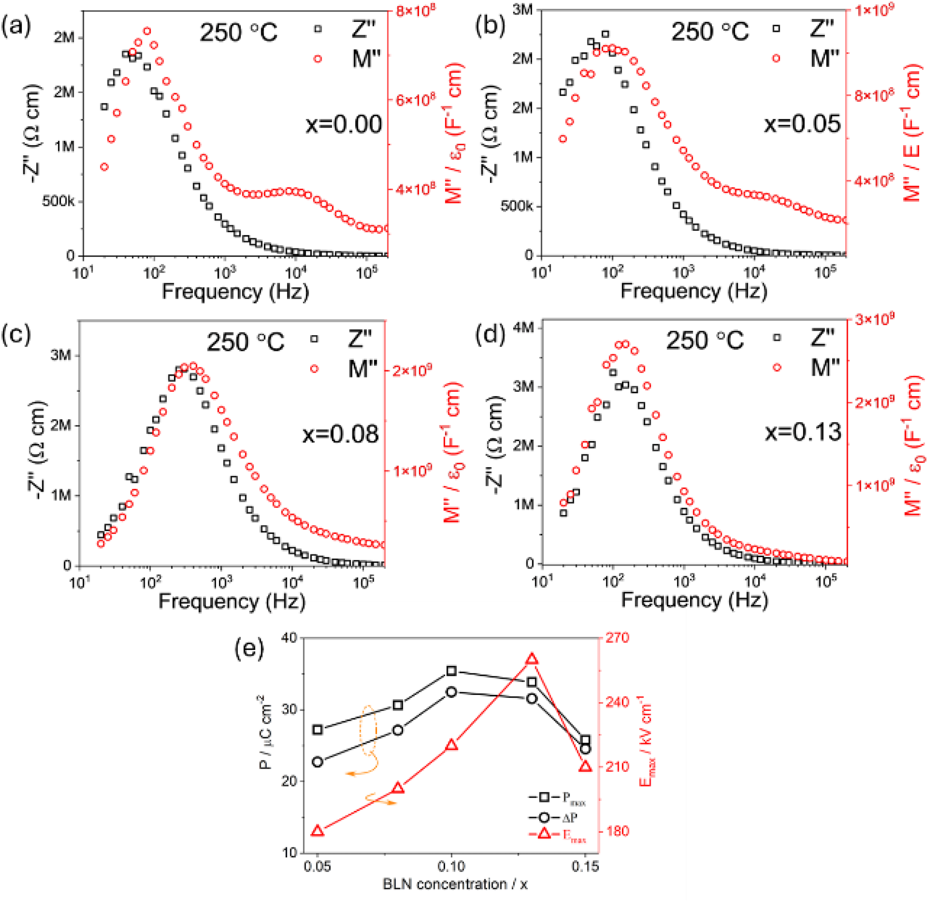
The influence of BLN on the electrical properties of (0.7 – x)BiFeO3-0.3BaTiO3-xBi(Li1/2Nb1/2)O3 ceramics. -Z″, M″ spectra for x = 0 (a), 0.05 (b), 0.08 (c) and 0.13 (d) at 250 oC. Pmax and Emax versus xBLN from P-E loops (e). Figure adapted from ref Wang et al. 7
(0.9-x)NaNbO3-0.1SrTiO3-xLa(Mg1/2Ti1/2)O3 for x = 0 and 0.02. 20
The third example is the influence of a ternary compound, La(Mg1/2Ti1/2)O3 (LMT) on a homogeneous electrical microstructure, Figure 6. NaNbO3 is a prime candidate as a dielectric material as it has one of the highest band gaps, 3.4–3.5 eV amongst all ferroic oxides. The binary system 0.9NaNbO3-0.1SrTiO3 is both electrically resistive and electrically homogeneous based on IS data. It requires temperatures > 450 oC to acquire meaningful data. The total resistivity of the ceramics are ∼ 160 kΩcm at 530 oC, Figure 6(a) and there is a single (and overlapping) Debye peak in the -Z″, M″ spectra, Figure 6(b), indicating that the total resistivity is associated with the grains (bulk). The Arrhenius plot of the bulk conductivity has Ea ∼ 0.9 eV which is a value commonly reported for extrinsic conduction in BT and ST-based ceramics, Figure 6(e). In this case, the addition of the ternary compound LMT is primarily to increase the bulk resistivity (or lower the conductivity) by at least one order of magnitude and to increase Ea to ∼ 1.3 eV, Figure 6(e). It has no influence on the electrical homogeneity, Figure 6(c) and (d). The increase in Ea indicates a clear change in the conduction mechanism but isn’t close to intrinsic (band gap) conduction given the band gaps of 3.5 and 3.2 eV for NN and ST, respectively. Possible conduction mechanisms are given in the discussion. Nevertheless, the high IR in these NN-based materials lead to impressive BDS that exceed 500 kV/cm.
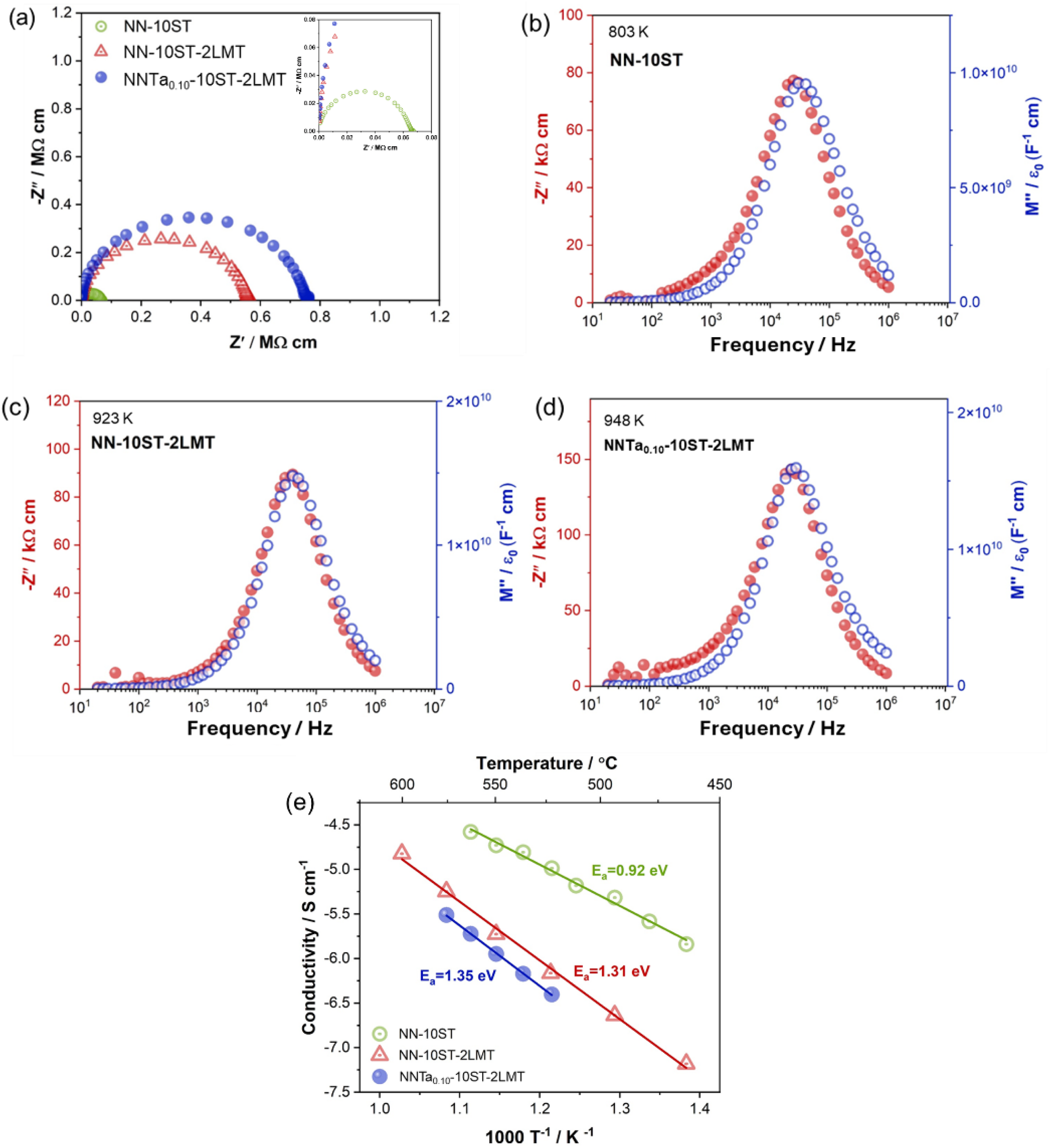
Z* plots and -Z″, M″ spectra for (0.9-x)NaNbO3-0.1SrTiO3-xLa(Mg1/2Ti1/2)O3 for x = 0 at 803 K (a,b) and 0.02 at 923 K (a,c). Impedance data for the QLD material 0.88[Na(Nb0.9Ta0.1)O3]-0.10SrTiO3-0.02La(Mg1/2Ti1/2)03 at 948 K is included for comparison (a,d). Arrhenius plots of bulk conductivity for all three ceramics (e). Figures adapted from ref Wang et al. 20
Octahedral tilting in ferroic oxides
A) Tilting in perovskites and TTBs
A classification and notation for tilting in perovskites was proposed by Glazer 46 who described tilting as component rotations about the three orthogonal axes. a, b and c denoted the magnitude of each tilt about the [100], [010] and [001] axes of a nominally doubled simple cubic cell. If tilting occurs equally about the axes, this is denoted by repeating the letter, such that ‘aaa’ refers to equal tilts and ‘abc’ unequal tilts about each axis. Tilting in-phase and in antiphase around each axis is described with a superscript ‘+’ or ‘-‘, respectively. The absence of tilt around a given axis is relayed by using the superscript ‘0’. a−a−c+ therefore refers to a perovskite with antiphase tilting about the pseudocubic a and b axes and in-phase around c, Figure 7. If a structure such as the AFE P phase in NaNbO3 has a complex or compound tilt around a given axis, a mixed superscript notation is applied, -/+, to give a−a−c+/− which indicates that the c-axis, has alternating sets of two in-phase tilted octahedra rotated in antiphase, Figure 8. 46
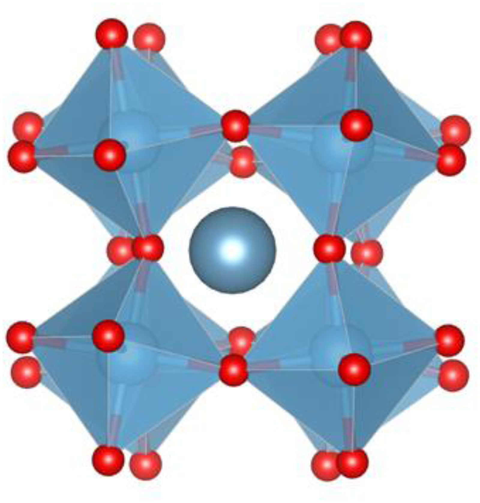
Crystal structure of the fundamental cell of CaTiO3 which has an a−a−c+ glazer tilt 46 system.
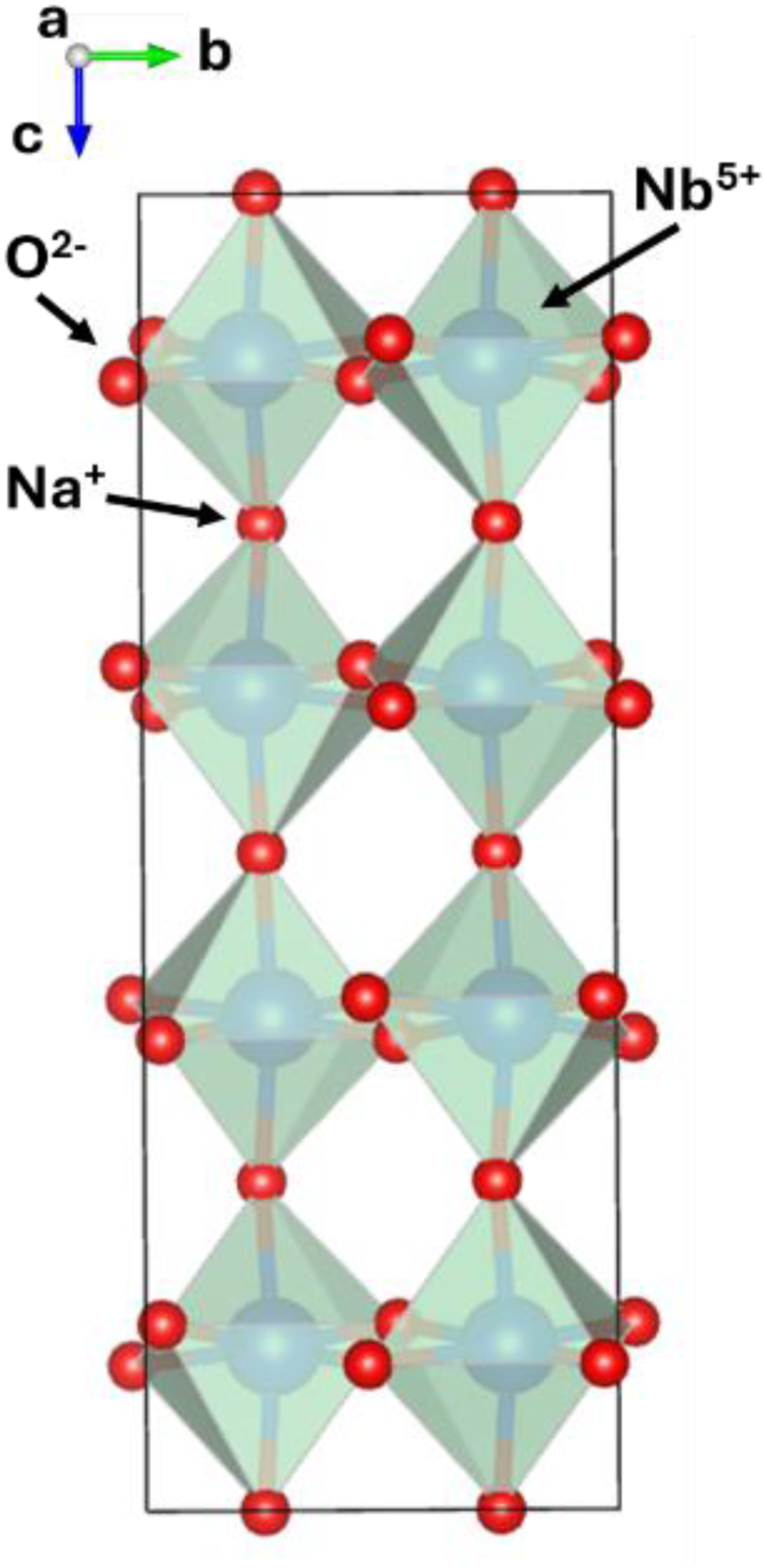
Structure of the P phase of NaNbO3 in which the octahedral framework (a−a−c+) has a √2a, √2a, 4a cell where a is the lattice parameter of the fundamental cubic cell.
For tetragonal tungsten bronzes, tilt configurations are influenced by the non-orthogonal bonding in parts of the octahedral network in contrast to perovskites in which the prototype bonding is orthogonal, Figure 9, creating trigonal, square and pentagonal sites in a [001] projection. 47 The known octahedral tilted supercells are complex (Figure 10) with many exhibiting incommensurate superstructure. 43 Commensurate superstructures are observed for compounds in which the A1-cation is too small for the cuboctahedral volume (square site) with Sr4Na2Nb10O30 exhibiting the largest reported superstructure. 47
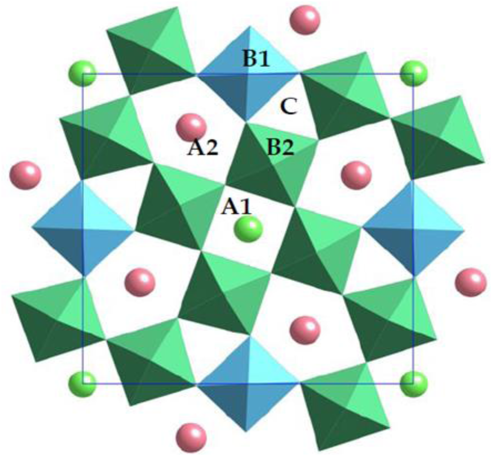
[001] projection of the octahedral framework (B1, B2) of the tetragonal tungsten bronze structure showing trigonal (C), square (A1) and pentagonal (A2) sites. Figure adapted from ref Zhu et al. 47
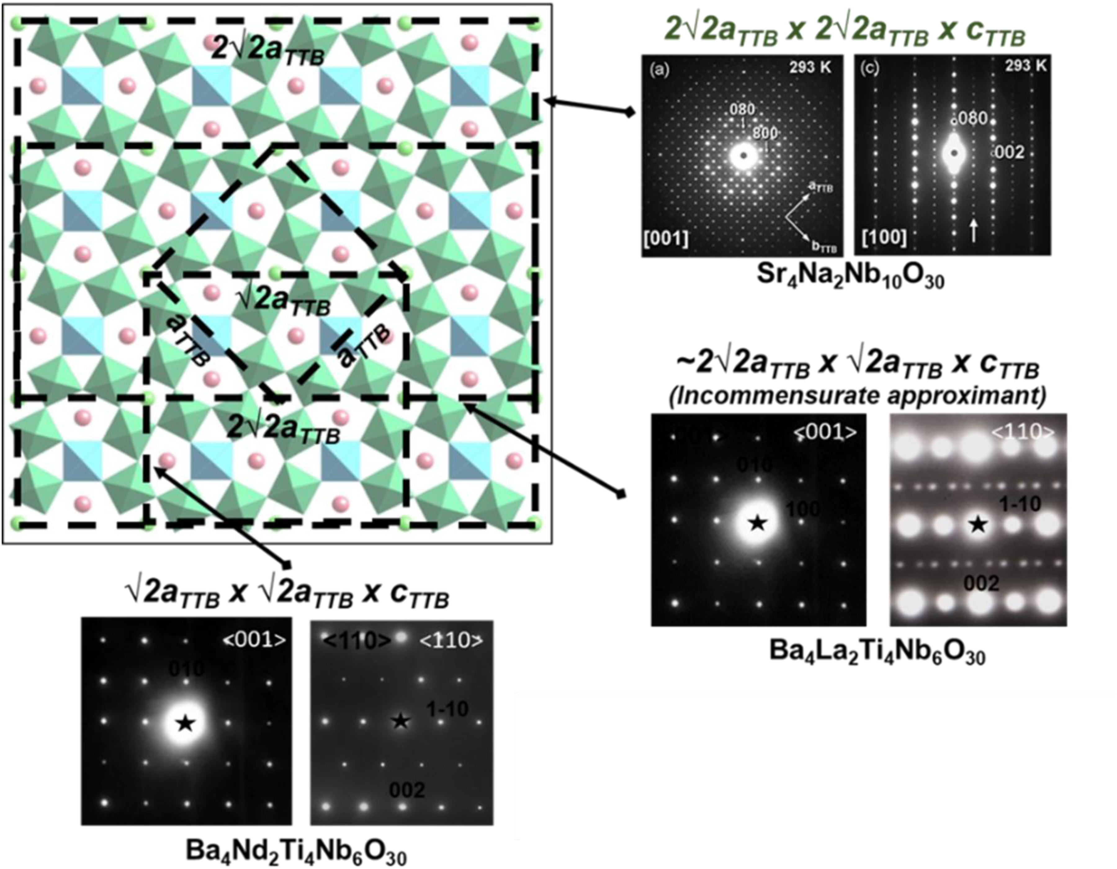
Octahedral tilt supercells in TTB structured ceramics.
A cornerstone of the following examples and the following discussion is the concept of octahedral tilt disorder or frustration. In the context of this article, octahedral tilt disorder/frustration is defined as local changes in the amplitude and/or type of octahedral tilt rotation on a nanoscale.
B) Worked examples of frustrated octahedral tilt systems
Quasi linear dielectric NaNbO3 based ceramics 20
Recently, NaNbO3 has attracted attention for the development of ceramics for high energy density capacitors due to its large band gap and therefore high intrinsic BDS. In a recent study by Wang et al.,
20
NaNbO3 (AFE, P phase) was initially modified with SrTiO3 (0.9NaNbO3 – 0.1SrTiO3, NN-ST) which resulted in stabilisation of the FE Q phase which is polar but has the same octahedral tilt structure as CaTiO3 (Figure 7). Compositions were subsequently modified through the addition of third perovskite member (0.88NaNbO3 – 0.1SrTiO3 – 0.02LaMg1/2Ti1/2O3, NN-ST-LMT) to reduce the scale length of polar order to give a relaxor phase.
20
Finally, polar order was further constrained through the partial substitution of Ta for Nb (0.88NaNb0.9Ta0.1O3 – 0.1SrTiO3 – 0.02LaMg1/2Ti1/2O3 (NNTa0.1-ST-LMT) which resulted in a near linear polarisation field loop and a room temperature paraelectric or quantum paraelectric state at RT. The compositional changes resulted in a decrease in the scale length of polar order from FE to REF to QLD but with a negligible change in perovskite in tolerance factor (t)
Q-NN MLCCs fabricated using Pt internal electrodes gave rise to exceptional Emax (>2000 kV/cm), energy density (> 40 J/cm3), temperature stability matching several EIA criteria that could operate at > 200 °C and 106 cycles at 1500 kV/cm, Figure 11. 20 The authors of ref Sarkar et al. 16 postulated that frustration related to competing structural phase transitions (anti-polar/polar/octahedral tilting) inhibits cooperative displacements from unit cell to unit cell. The absence of cooperative polar displacements ensures that a conventional domain structure does not occur (even under high field) and therefore cooperative switching, typically observed in FE (microdomains) and REL (nanodomain) phases (Figure 1) is absent, preventing saturation in P-E loops. The complex solid solution also, as discussed, in the worked examples in section 2, also promotes a large BDS.
Bulk P-E loops from NN-ST based ceramics and unipolar P-E loop from a Q-NN multilayer. Figure adapted from ref Wang et al. 20
Further evidence for octahedral tilt frustration, above that shown in ref Wang et al. 20 , is presented in Figure 12 which shows <001 > zone axis diffraction patterns from a NNTa0.1-ST-LMT ceramic with 4 distinct regions of a grain, exhibiting P phase, Q phase and two types of incommensurate structure as evidenced by streaking in the [010] direction. The incommensurate superstructure is attributed to tilt disorder arising from frustration between the 4xP and 2xQ phase. The two images in Figure 12 demonstrate at a microscopic level how the reciprocal space superstructures in the diffraction patterns appear as disordered features and defects in real space, consistent with the above arguments.
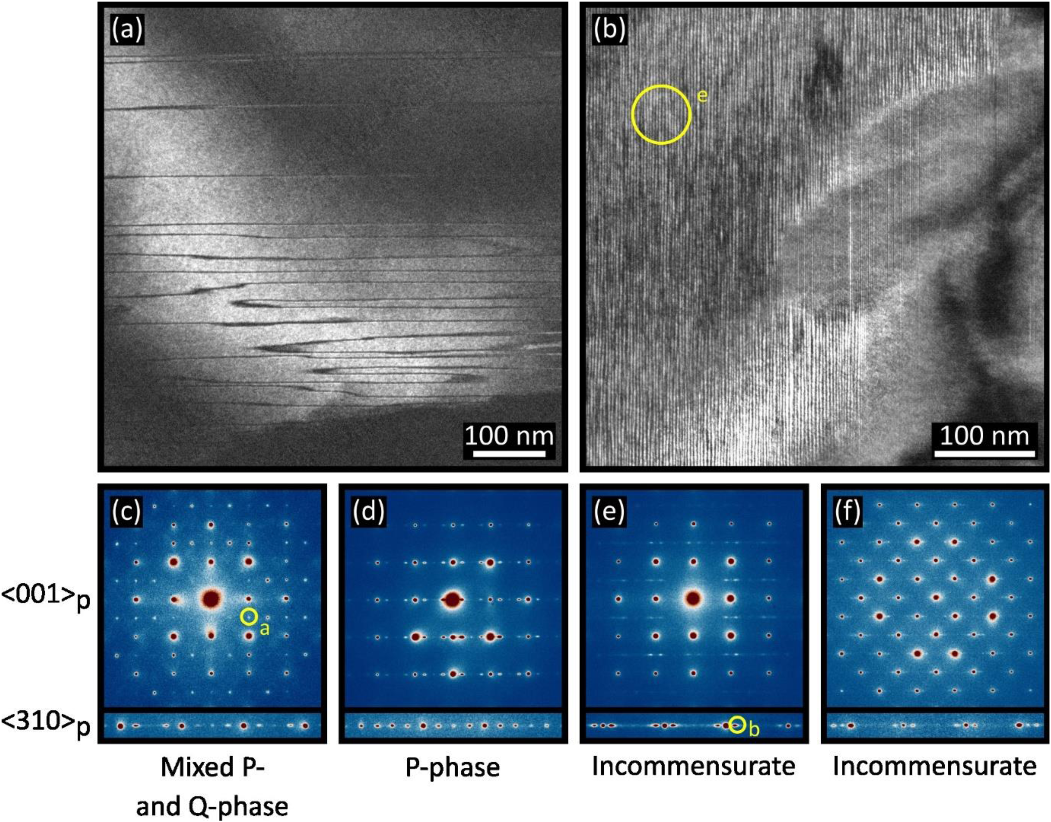
Dark field images from a single grain showing regions of a) antiphase boundaries associated with anti-parallel cation displacements (Q phase) and b) incommensurate superstructure. c-f) <001> zone axis electron diffraction patterns and superstructure reflections in the <310> from different regions of a grain of Q-NN ceramic. The diffraction pattern presented in (e) was recorded from the region indicated in (b) and Dark Field micrographs (a) and (b) were generated by selecting the diffraction spots indicated in (c) and (e), respectively.
Short-range ordered tilting in the Na1/2Bi1/2TiO3 weakly coupled relaxors 21
The unipolar P-E loops for NBT-SBT-xBMN ceramics at the maximum applied electric field (Emax) are shown in Figure 13. Both Wrec and η are significantly enhanced with an increase in BMN concentration, with a maximum Wrec of ∼7.5 J/cm3 achieved at x = 0.08. Along with the large Emax, resulting from improved resistivity and electrical homogeneity, a large ΔP (∼46 μC/cm2, large Pmax∼48 μC/cm2 and small Pr∼1.5 μC/cm2 contribute to the Wrec and η, effectively describing an ideal ultra-slim P-E loops (Figure 12(d)) which does not fully saturate as field increases. 21 Figure 14 shows in-situ dark-field, two-beam superlattice TEM images obtained as a function of temperature using ½{hk0} in-phase tilt reflections and the accompanying [001] selected area electron diffraction patterns for x = 0.08 recorded at RT. Also included in Figure 14 is a < 110 > zone axis diffraction pattern which reveals ½{hkl} superstructure reflections, arising from antiphase tilting, but the absence of ½{hk0}. For <110 > zone axes, although reflections of the general type ½{hk0} reflections are permitted, the Weiss Zone Law dictates an extra condition such that h = k. For in-phase tilt reflections, h ≠ k and are therefore, forbidden in the <110 > . 21 For perovskites with t < 0.98, (NBT-SBT-0.08BMNN), combinations of in-phase and antiphase rotations are predicted based on geometric arguments by Glazer 42 and Reaney et al. 48 The most likely explanation therefore, for the presence of ½{hk0} and ½{hkl} superstructure reflections in electron diffraction patterns is the coexistence of in-phase and antiphase tilting. Mixed tilt systems which combine in-phase and antiphase rotations are a+b+c−, a+a+c−, a+b+b−, a+a+a−, a+b−c−, a+a−c−, a+b−b−, a + a-a-, a0b−b+ and a0b−c+. Howard and Stokes 49 utilised group theory to combine polar displacements with mixed tilting and established 11 possible space groups, Ama2, Amm2, Cmc21, Cc, P42mc, Aba2, Pna21, Pmc21, Pmn21, Pc, P21 and Pm which
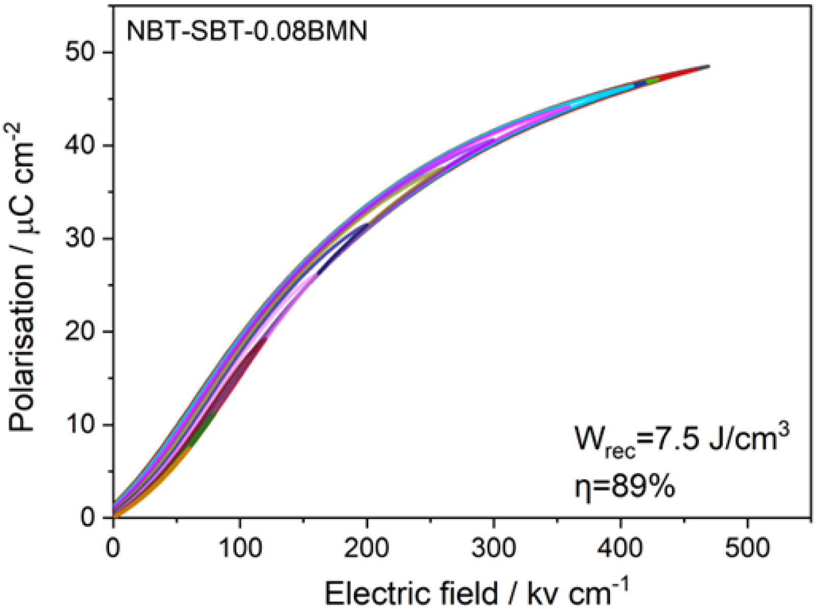
Unipolar P-E loops from NBT-SBT-BMN based ceramics as a function of BMN concentration. Figure adapted from ref Ji et al. 21
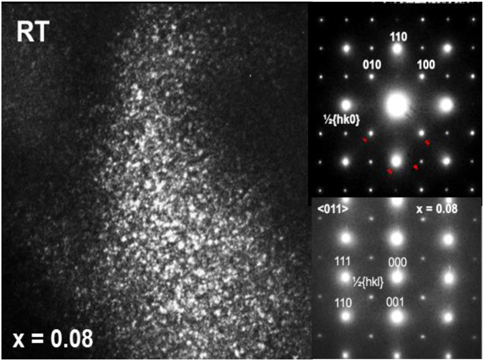
Dark field image show SRO tilted region in NBT based ceramics. <001> and <110> zone axis electron diffraction patterns indicating the presence of octahedral rotation in and out of phase. Figure adapted from ref Ji et al. 21
therefore, describe the possible local polar structure in NBT-SBT-0.08BMN, all of which are either tetragonal (T), monoclinic (M) or orthorhombic (O). This complex local symmetry creates frustration and disorder above that associated uniquely with the distribution of cations through the perovskite lattice. The effect on the P-E curve is to, not only induce a slim relaxor response, but also to increasingly inhibit saturation, in a manner reminiscent of that observed for Q-NN ceramics 20 which also have multiple hierarchies of disorder. Once again, the correct choice of doping and alloying substitutions simultaneously induces a frustrated octahedral tilted and point defect state that favour high energy density through a combination of a high BDS accompanied by limited saturation of the P-E loop. These methodologies for weakly coupled relaxors have been repeated in a large number of systems in which a lower tolerance factor end member has been introduced into a relaxor system, many of which are described in ref Wang et al. 8 .
Nb-based tetragonal tungsten bronze structured ceramics 50
The authors of ref Duan et al. 50 substituted Na+, Ca2+, Bi3+ (A1/A2-sites) and Ta5+(B-site) to induce structural frustration within (Sr1/2Ba1/2)2Nb5O15 (SBN-H) TTB structured ceramics. They reported disruption to long-range ferroelectric order due to compositional fluctuations which created polar nanoregions (PNRs). They proposed that the high entropy (disorder) in the system reduced the domain-switching energy barriers and weakened domain intercoupling. They achieved a large Wrec of ≈10.6 J cm−3 and ultrahigh η ≈ 96.2% at 760 kV cm−1 and suggested that there was a commensurate improvement in mechanical properties, Figure 15. 50
Unipolar P-E loop from SBN-K. Figure adapted from ref Duan et al. 50
Although there is significant disorder in the system, there is no evidence of enhanced solid solution based on a high entropy effect alluded to by the authors of ref Duan et al. 50 , since all dopant ions are known to substitute onto the A1/A2 and B1/B2-sites, based on other TTB structured ceramics. 47 However, there is no doubt that they have achieved exceptional values of Wrec and η. Most strikingly, the almost linear behaviour of the P-E loop is similar to the QLD perovskites reported by ref Wang et al. 20 with a large Emax (high BDS). In TTB structured ceramics, there is already intrinsic disorder based on frustration between the Nb displacements within the B1 and B2 sites with a general trend towards relaxor behaviour which is only overcome (i.e., when FE order dominates) if there is a large average A1/A2 site ionic radius or through a change in the octahedral tilt framework when there is a small A2 site ion. 47 The authors of ref Duan et al. 50 do not consider the octahedral framework in their argument. Based on previous studies in ref Zhu et al. 47 , ‘high entropy’ TTBs will have an incommensurate superstructure consistent with the Labbe approximant (Figure 10). Therefore, we propose an alternative perspective/explanation to describe their exceptional dielectric behaviour; tilt disorder further limits polar coupling at high field resulting in quasi-linear P-E behaviour similar to NBT 21 and NN 20 based ceramics, in part due to intrinsic incommensurate behaviour but also the ionic radii distribution on the A1/A2 sites. In addition, the ‘high entropy’ A-site dopants in SBN (Na, Ca and Bi) along with Ta on the B-site create a defect state that enhances BDS. There is no new physics required to explain the large Wrec, only structural frustration which inhibits polarisation saturation, coupled with the ability to apply a large field due to a high BDS.
Discussion
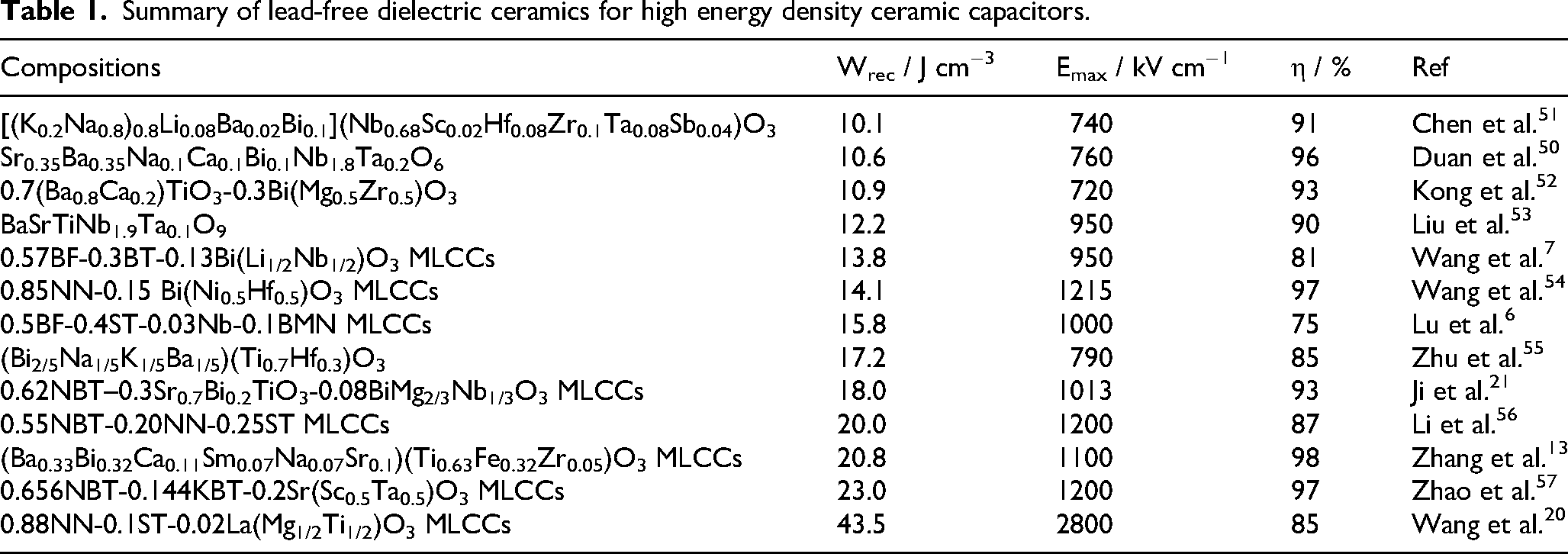
The work reviewed previously clearly indicates the importance of the defect chemistry and stoichiometric dopants in controlling the breakdown strength (high Emax) and also the role of short-range octahedral tilt disorder in creating systems which do not readily saturate at field and which therefore achieve high Wrec through increasing E. All thick film (powder) based systems which achieve ultra-high Wrec to date correspond to these two criteria which implies that they are key design metrics in optimising high permittivity and voltage MLCCs for power electronics. Key parameters of recent reported materials were summarised in Table 1 below. In the following, we expand upon and discuss the mechanisms by which the conductivity is minimised through the use of stoichiometric dopants and how such dopants in combination with a t < 1 matrix create short range ordered tilting which limits the saturation of the P-E loop with increasing E.
Summary of lead-free dielectric ceramics for high energy density ceramic capacitors.
A) How short-range tilting suppresses saturation of the P-E loop
In its simplest form saturation of a hysteresis loop in ferroelectrics occurs when all ferroelectric dipoles are aligned with the direction of the applied electric field. This concept is complicated by microstructural factors such as the grain and domain structure, the multiple orientations of which can limit the direction of the alignment with only a vector of the dipole aligned with the field. Nonetheless, once all the possible re-orientation has occurred, the polarisation is saturated. For imperfect ferroelectrics which exhibit the reorientation of space-charge regions under field, saturation may not be completely achieved as charge may continue to move under the field once the FE-dipoles have reoriented. Since ceramic ferroelectrics all contain space charge regions, a hysteresis loop is often modelled by considering these two types of polarisation with a space-charge hysteresis loop superimposed onto a FE dipolar loop, the relative fractions of which dictate the quality of the FE ceramic.
Relaxor ferroelectrics are composed of polar nano regions (PNRs) rather than long range ordered macrodomains, typical of a FE.6–12 PNRs can behave in several different ways under large applied fields. Some undergo a relaxor to ferroelectric transition in which the field causes the PNRs to coalesce with the polarisation aligning direction of the applied field, to create long range FE order. 58 As a result, the P-E loop widens as field increases, commensurate with the extent of PNR coalescence. In weakly coupled relaxors, there is negligible coalescence and the PNRs act largely independently. Their small size ensures that there is minimal energy involved in their reorientation and the loop is slim, even at high field. Nonetheless, there is a finite number of PNRs which when reoriented cause the polarisation to either saturate or tend towards saturation.
Classic linear dielectrics have no polar dipoles to reorientate and charge is stored through mainly ionic polarisation, hence it does not saturate except theoretically under extreme fields well beyond the BDS. Linear dielectrics also are imperfect and reorientation of space-charge defect regions causes the loop to widen, often referred to as a ‘lossy dielectric’. The abiding property of a linear dielectric (class 1) is that it has low permittivity 4 since there is a negligible re-orientation of charge in comparison with FEs and relaxors.
Despite these text book definitions which are often utilised to explain dipolar behaviour, it is perhaps more instructive to view linear dielectrics, 4 weakly coupled relaxors, 21 relaxors6–12 and ferroelectrics as 4 regions on a continuum along an axis of average ionic polarisability, Figure 16, in which from right to left the degree of saturation decreases. The boundaries between the regions are not distinct and are for illustrative purposes only. They will also depend on factors such as the magnitude of the dipolar displacement in the base material and in the dopants with lone pair electrons (Bi3+ and Pb2+) typically displacing off-centre in their polyhedral cage more than d0 ions (Nb5+ and Ti4+). Typically, from right to left there is a marked decrease in the polarisability of the constituent ions which leads to a decrease in ionic displacement, polar coupling and a reduction in permittivity. However, this general principle can be affected by secondary factors such as the amplitude and scale length of octahedral tilting.20,21,50 Within a disordered octahedral framework, polarisable ions such as Ti, and Bi can displace off centre, contributing to the permittivity but do not strongly couple to adjacent regions since they have a different tilt configuration (and therefore crystal structure) which frustrates polar coupling and therefore inhibits saturation. When introduced into the diagram the effective linear region is displaced to the right and the permittivity remains far higher than in conventional linear dielectric such as Al2O3, resulting in a new class of QLDs.20,50
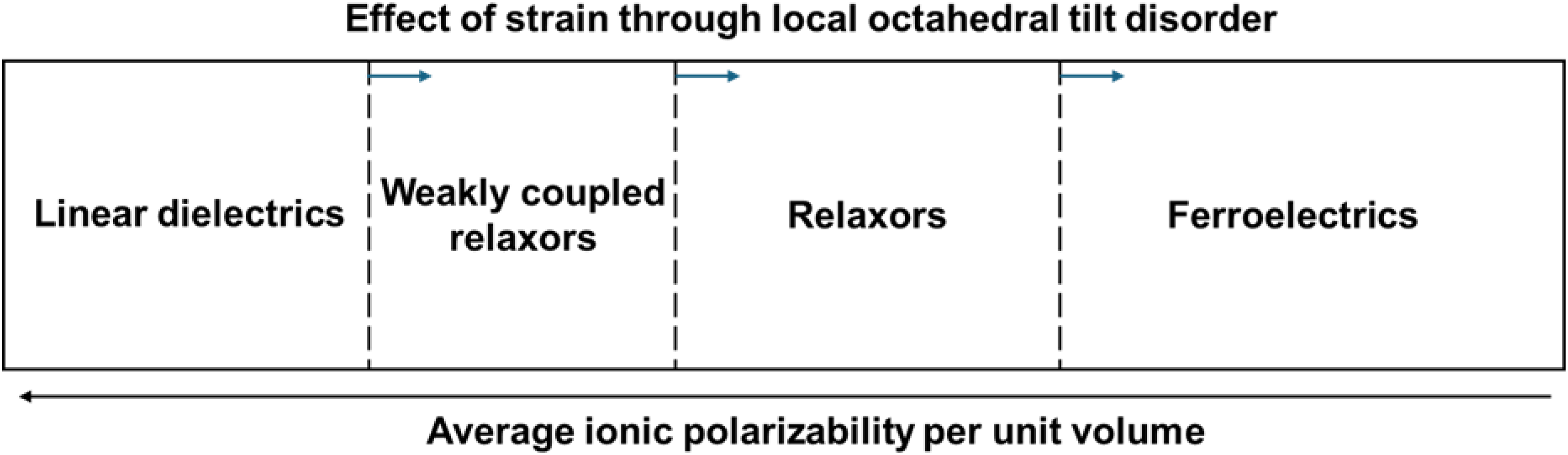
Schematic illustrating the scale length of polar order and relevant dielectric behaviour.
The advantage of a high permittivity linear material is that the polarisation continues to increase with field, giving rise to a greater area to the left of the P-E loop as E increases and therefore ever greater energy density. The absence of saturation therefore has tremendous benefit for energy density, provided the material does not break down. To maximise energy density therefore, it is important to have t < 1 for the perovskite matrix so that the systems are distorted through octahedral tilting in addition to polar or antipolar behaviour or, as in the case of TTBs, have intrinsic octahedral frustration along with polar behaviour.
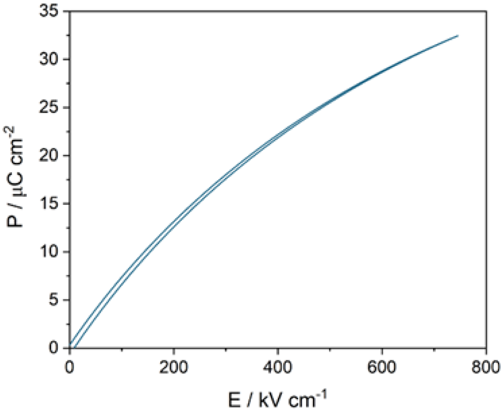
One further advantage of QLDs arising from local frustration/competition is the absence of domain switching associated with an FE or a field induced transition typical of many relaxors and antiferroelectrics. Field induced transitions result in a macrodomain state and give rise to large strains. For example, the field induce transition in PbZn1/3Nb2/3O3-PbTiO3 ceramics can give rise to up to 0.6% strain 59 which in an MLCC geometry, this would lead to fracture at the grain boundaries and delamination at the metal ceramic interface under cycling. In contrast even at extreme fields, the strain of the NN-based QLD materials in ref Wang et al. 20 does not exceed 0.1% which is much less than a typical PZT (0.2%) 60 and may be accommodated within the multilayer structure.
In summary, the dopants/alloying substitutions must not only induce local perturbations in the crystal structure and limit strain but also enhance BDS. Fortunately, t < 1 matrix materials (e.g., BF, NN, NBT) are common and there is a wide choice of dopants and alloying additions that can maintain t < 1 with many cations having the necessary size and valence to frustrate field induce behaviour and enhance IR and BDS in the manner discussed below.
B) Influence of multiple site occupancies on IR and BDS
Three IS examples from the complex perovskite systems described in section 2 illustrate how multiple ion site occupancies can be used to enhance IR and/or BDS of electro ceramics based on changes in the electrical heterogeneity and/or in the predominant conduction mechanism(s). At the outset it is worth noting that ABO3 is an average composition and that heterogeneity on a local scale exists where the A/B stoichiometry can deviate from =1 and/or local oxygen content is <3. In all of our examples, intrinsic electronic conduction is never fully achieved and the contribution(s) from ionic conduction, and in particular residual oxygen vacancies (or possibly Na vacancies in the case of NaNbO3) play a significant role in the conduction mechanisms, either directly or indirectly. Although the measured bulk conductivity by IS may be dominated by either electronic or ionic conduction, a framework based on mixed ionic-electronic conduction, is often a better reference point, as explained below.
(i) and (ii) are good examples of systems that make use of BiFeO3 being the major perovskite component (>60 mol%) and given its smaller band gap and higher leakage conduction than (Ba,Sr)TiO3-based perovskites the IR of the bulk component in these ceramics is dominated by the defect chemistry of BiFeO3 and the ceramic processing conditions. In both cases, the inclusion of Nb2O5 as a third component, either as additions of Nb2O5 (example (i)) or replacement of Fe by Li/Nb on the B-sites (example (ii)) has a significant influence on the bulk conductivity and therefore improvement of IR and/or BDS. In the case of (i), there is a dramatic decrease in bulk conductivity and a change in conduction mechanism, Figure 4(f) with low levels of Nb2O5 additions which produces the higher IR. In the case of (ii), IR is not strongly influenced by the Nb-content but it does have a dramatic effect on the electrical homogeneity of the grains, see -Z″/M″ spectra in Figure 5 which improves the BDS, Figure 5(e). Furthermore, ceramics of x = 0.00 for example (i) [60BF:40ST] were sintered in the range 1070 −1100 oC with IR ∼ 180 kΩcm at RT, Figure 4(a) whereas for those of x = 0.00 for example (ii) [70BF:30BT] were sintered < 1050 oC and IR exceeds ∼ 4 MΩcm at 250 oC, Figure 5(a). This shows the ceramic processing conditions (in the absence of Nb doping/additions) are important and can produce different levels of defects and distribution of ions on a local scale.
In example (i) the lowering of the bulk conductivity by several orders of magnitude and the switch in Ea from ∼ 0.4 to ∼ 1.2 eV with increasing x can be explained based on the defect chemistry described above for processing of BiFeO3-based ceramics with the loss of Bi2O3 and B-site donor doping by Nb ions that can compensate for the oxygen vacancies generated. The high bulk conductivity and low Ea of x = 0.00 is dominated by extrinsic p-type electronic conduction (Fe3+/Fe4+); however, there are residual oxygen vacancies present and although the ionic contribution to the conductivity (at least in air) is low, it remains present and these ceramics are mixed ionic-electronic conductors. Donor doping with low but sufficient levels of Nb is effective in reducing the level of oxygen vacancies created during sintering and therefore limits the level of oxygen gain on cooling that generates the partial oxidation of Fe3+ to Fe4+ and therefore suppresses the extrinsic p-type conduction. Ea for the bulk conduction in x > 0 ceramics is ∼ 1.2 eV which is still below that expected for intrinsic conductivity across the band gap and indicates the bulk conduction mechanism may still include a low-level ionic contribution associated with oxygen vacancies. This is probably unsurprising, as on a local scale there may be some regions of above average acceptor-doping of Sr for Bi on the A-sites beyond the intended, nominal ABO3 stoichiometry (i.e., Bi1−xSrxFe1−xTixO3) based on compensated acceptor (A-site Sr) and donor (B-site Ti) doping of the perovskite lattice and this can create oxygen vacancies (i.e., O < 3); however, their mobility and ability to contribute to long range migration is limited to high temperatures/electric fields.
In example (ii), the base binary material (x = 0) contains more BiFeO3 than in example (i), yet the ceramics are more insulating. The primary reason for this is the lower sintering temperature of ceramics in example (ii) compared to example (i). This produces less Bi2O3 loss which creates less oxygen vacancies on sintering and therefore lower levels of oxygen gain on cooling and therefore less partial oxidation of Fe3+ to Fe4+ to create the high bulk conductivity observed for x = 0 in example (i). However, it is noteworthy that there is clear evidence of electrical heterogeneity in the bulk component of example (ii), see M″ spectra in Figure 5(a); and that the smaller M″ peak at higher frequencies is consistent with leaky p-type regions associated with partial Fe3+/Fe4+ electronic conduction. These conductive regions are detrimental to BDS and, as in example (i) an increasing amount of Nb via the third perovskite component permits an increasing level of Nb-donor doping (via ionic compensation, i.e., oxide ions as opposed to electronic compensation) that is effective in suppressing this conduction mechanism and results in the grains becoming increasingly electrically homogeneous, see M″ spectra in Figure 5(c) and (d) and the improvement in the dielectric behaviour is reflected in an increase in the BDS for x > 0.05 without any significant change in the grain size, Figure 5(e).
In case (iii), NaNbO3 is the major component of the solid solution and therefore dominates the electrical conduction properties. There is little literature and knowledge on the defect chemistry and the influence of acceptor and donor dopants on the bulk conductivity of NN and other I-V perovskites (e.g., KNbO3) compared to many II-IV (e.g., SrTiO3, BaTiO3) and III-III (e.g., LaGaO3) perovskites. In this case, there is a potential issue with volatilisation of Na2O during ceramic processing which can induce Na and O vacancies which may lead to either or both cation (Na) and/or anion (O) conduction in addition to any electronic conduction. It should be stressed that undoped NN ceramics are generally more resistive than BF based ceramics not only due to the higher band gap but also because there are no oxidisable cations in NN and any gain in oxygen on cooling from the filling of oxygen vacancies cannot generate the leaky, low Ea p-type semiconductivity observed in BF-systems where Fe3+ can be oxidised to Fe4+. Any oxygen gain has to result in partial oxidation of the anion, i.e., O2− to O− and this generally gives rise to a low level of p-type extrinsic conductivity along with the presence of oxygen vacancies. This type of mixed conduction is also observed in other dielectric perovskites such as undoped BaTiO3 and SrTiO3 with Ea typically ∼ 0.8–0.9 eV.26,27
Undoped NN has limited A/B non-stoichiometry but this doesn’t lead to the same dramatic switch from electronically insulating to high oxide ion conductivity as observed for NBT. The changes are more modest with NN retaining good dielectric behaviour up to ∼ 400 oC 61 but there have been reports of undoped NN prepared by Spark Plasma Sintering (SPS) being predominantly a Na ion conductor. 62 For dopant studies, there are reports of acceptor-type Ti-doping on the B-site (again by SPS) inducing O vacancies and increasing the level of oxide ion conductivity, 62 whereas donor-type Sr-doping on the A-site induces A-site vacancies with only modest changes in the bulk conductivity. 63 In the former case, the doping limit is ∼ 5 at% whereas in the latter it is ∼ 20 at% and these results suggest that oxygen vacancy migration is more facile in NN than Na ion migration but further studies with a wider range of dopants are required to substantiate this hypothesis.
For nominally stoichiometric x = 0 in example (iii) the bulk conductivity is low until > 400 oC and the associated Ea is consistent with that described above for mixed ionic-electronic conduction. The inclusion of the third perovskite does not influence the electrical homogeneity based on -Z″, M″ spectra, Figure 6(b)–(d) but has a significant effect in reducing the bulk conductivity, increasing both IR and the associated Ea, Figure 6(e). If the donor-acceptor compensated mechanism of La(Mg1/2Ti1/2)O3 20 is consistent on a local scale then no new defects are created and only a small (if any) change to the band gap would be expected for such a low level of the third component. Therefore, no significant changes in bulk conductivity would be expected. Based on the limited available information on the defect chemistry of NaNbO3, the influence of individual ions that might occur locally on the A and B-sites of NN would be creation of A-site vacancies on La (donor) doping and oxygen vacancies on Mg, Ti (acceptor) doping, respectively; however, these are unlikely to contribute to long range migration.
The most plausible explanation for the suppression of the conductivity is the creation of deep potential energy wells in the saddle points (i.e., bottlenecks) associated with the oxide-ion migration pathway between two A-sites and a B-site ion in the perovskite lattice, Figure 3. The addition of the third component (ignoring Ta in the optimised QLD material) results in a distribution of three different sized A-site [Na (1.39 Å), Sr (1.42 Å) and La (1.36 Å)] and B-site cations [Nb (0.64 Å), Mg (0.72 Å) and Ti (0.605 Å)] which creates localised strain linked to the octahedral tilting networks. This variance in cation size, mass, polarisability and bond strength to oxygen on a local scale suppresses the long-range migration of oxide ions and reduces the level of ionic conduction in these materials, both in terms of carrier concentration (n) and mobility (μ), given σ = nqμ where q is the charge on the carrier. This leads to materials where the ionic contribution to the mixed bulk conductivity is heavily suppressed, but it is interesting to note that the Ea of ∼ 1.3 eV is substantially less than that expected for intrinsic electronic conduction. This indicates the bulk conduction mechanism(s) in these ternary based materials to be complex and worthy of further investigation. What is clear, is there are no significant donor or acceptor electronic doping mechanisms that give rise to high levels of n- or p-type (electronic) semiconductivity with low Ea (i.e < 0.4 eV) in these NN-based materials.
The variance in mass of the multiple cations and their different bond strengths to oxygen influence the local vibrations (and therefore phonons) that contribute to the mobility of both the electronic and ionic conduction carriers in these materials. This influences both the measured electrical and thermal conductivity in these materials and may not only increase IR but also reduce self-heating and thermal runaway. Further studies are required but a phonon-glass approach using multiple cations and vacancies in perovskite and TTB lattices is a well-established mechanism in lowering thermal conductivity in thermoelectric oxides. 64 Although it is beyond the scope of this script, future studies should investigate both the electrical and thermal conduction mechanisms in these materials to ensure optimisation in suppressing IR and thermal runaway whilst maximising BDS.
Conclusions and future directions
In this script we demonstrate two key design metrics in multivalent polar/anti polar perovskites (with t < 1) and polar TTBs (with intrinsic octahedral frustration) to optimise high permittivity and voltage MLCCs for power electronics. First, the importance of controlling the defect chemistry and stoichiometric dopants in the perovskite materials to achieve homogeneous electrical microstructures to maximise the IR and BDS (high Emax). Second, the role of short-range octahedral tilt disorder in creating systems which do not readily saturate with electric field and which therefore achieve high Wrec through increasing E. Furthermore, we propose a synergistic effect between these two metrics as the local compositional disorder that creates the short-range octahedral disorder and lattice strain is effective in suppressing ionic conductivity (predominantly oxide ions) at high electric fields. As a consequence, the short range ordered tilting that produces quasi linear P-E behaviour can be exploited to higher E by high IR and enhanced BDS.
A key feature of this work is how (nominally stoichiometric) compositional change can decrease the scale length of polar disorder without significant changes in the average tolerance factor of the materials. The presence of mixed tilt systems with complex local symmetry creates frustration and disorder above that associated uniquely with the distribution of the cations through the perovskite/TTB lattice. We argue that the variance in the size and mass of the multiple cations and their different bond strengths to oxygen create the necessary strain to produce the desired quasi linear dielectric properties for high energy density applications. Coincidently, such situations often occur in multicomponent so-called ‘high entropy’ systems but invoking ‘entropy’ arguments does not attest to the underpinning crystal chemistry which leads high energy density/voltage dielectrics.
Future directions in high energy density ceramics are numerous and span from improved fundamental understanding, design and characterisation of QLD complex oxides to achieving materials that are compatible with existing BME MLCCs technology for scale-up of commercial applications. For materials development there is need to employ advanced characterisation methods to establish the local compositional and structural disorder in QLD perovskite/TTB oxides to garner better insight as to how they link with the electrical properties to inform on future design(s) to achieve optimisation. Given the importance of cation and anion displacements and octahedral tilting in these QLD materials, its imperative that techniques that can characterise both cation and anion sublattices on a local scale for dipolar mapping be employed. Good recent examples of this on NaNbO3-based materials are the use of total scattering methods65,66 and electron ptychography. 67 In addition, computational methods such as phase field simulations are becoming invaluable for understanding the evolution of polar domain structures as solid solutions are formed between two or more materials. For example, in the NaNbO3-Bi(Ni1/2Hf1/2)O3 system the long range ordered NaNbO3 AFE microdomains are broken into nanodomains embedded in a polar orthorhombic matrix with a certain orientation with increasing Bi(Ni1/2Hf1/2)O3 content. 54 It is clear that a combination of advanced experimental and computational methods is going to be required to answer many of the remaining scientific questions in the development of these more complex QLD materials. For example, what are the upper and lower limits to the polar disorder in these complex perovskite/TTB systems to achieve QLD and is there an upper limit to the permittivity that can be achieved? Can these QLD materials achieve the high permittivity (> 1000) values obtained in conventional FE and RFE?
Footnotes
Author contributions
Ian M. Reaney: Conceptualisation, Methodology, Investigation, Data Analysis, Writing-Original Draft, Writing-Review & Editing, Supervision
Richard Beanland: Methodology, Investigation, Data Analysis, Writing-Review & Editing
Robin Sjökvist: Methodology, Investigation, Data Analysis, Writing-Review & Editing
Yubo Zhu: Methodology, Investigation, Data Analysis
Ge Wang: Methodology, Investigation, Data Analysis, Writing-Review & Editing
Derek C. Sinclair: Conceptualisation, Methodology, Investigation, Data Analysis, Writing-Review & Editing, Supervision
Funding
The authors disclosed receipt of the following financial support for the research, authorship, and/or publication of this article: This work was supported by the Engineering and Physical Sciences Research Council, (grant number EP/Z536003/1). Ge Wang would like to acknowledge the financial support from Dame Kathleen Ollerenshaw Fellowship provided by The University of Manchester.
Declaration of conflicting interests
The authors declared no potential conflicts of interest with respect to the research, authorship, and/or publication of this article.