
Abstract
A high-performance cubic composite of tungsten (VI) oxide chloride/poly N-methyl pyrrole (WO2Cl2/PNMP) has been synthesized as a promsing n-type layer using a one-pot fabrication method. This innovative thin-film composite exhibits exceptional optoelectronic properties through the deposition on the p-layer of poly-1H pyrrole (P1HP) for the construction of WO2Cl2/PNMP/P1HP. The WO2Cl2/PNMP material features a distinct cubic crystalline structure with an optimal crystal size of about 11 nm, which enhances its structural stability and performance. A standout characteristic of the WO2Cl2/PNMP composite is its remarkable optical absorption in the visible (Vis) and ultraviolet (UV) regions, pivotal for its optoelectronic functionality. The device created from this composite achieved a peak current density under light (Jph) of approximately 0.39 mA cm−2. Additionally, the Jph values at photon energies of 3.6 eV and 2.3 eV were estimated at 0.34 mA cm−2 and 0.28 mA cm−2, respectively, emphasizing its effective photoconductive response. Furthermore, the device exhibited an optimized photoresponsivity (R) of 3.4 mA·W−1 at 3.6 eV, confirming its strong light-harvesting capabilities. The estimated detectivity (D) value of 0.75 × 10⁹ Jones at this photon energy further highlights its potential for high-sensitivity photodetection. In addition to its technical benefits, this optoelectronic thin film showcases the photodiode Schottky behavior, beside its economic feasibility, making it a practical option for cost-effective large-scale production. With its impressive optoelectronic performance, structural robustness, and scalability, the WO2Cl2/PNMP/P1HP-based device is highly recommended for industrial applications in optoelectronics, including photodetectors, sensors, and various light-responsive technologies.
Introduction
Photodetectors, or photosensors, are vital elements in contemporary electronic and optoelectronic technologies because they transform incoming light into electrical signals. Their uses extend across numerous sectors, such as telecommunications, industrial electronics, automotive systems, security, environmental monitoring, biomedical imaging, and water purification technologies. These multifunctional devices are key in detecting and analyzing light and electromagnetic radiation, permitting real-time monitoring and control in diverse industrial and scientific applications.1,2 The fabrication of these conjugated polymers with thermoplastic-like behavior enables efficient charge transfer, which is further enhanced under light illumination, thereby improving the performance of the photodetector.3–6
Photodetectors operate through various mechanisms, including photoemission, photoelectric effects, photochemical interactions, and thermal effects. Despite these differing principles, the core function of most photodetectors relies on generating electron-hole pairs when illuminated. When photons with energy exceeding the material’s bandgap hit the photodetector, they excite electrons from the valence band to the conduction band, creating positively charged holes. The electrons in the conduction band and holes in the valence band possess mobility, enabling them to diffuse and drift when an external electric field is applied.7,8 Without an applied field, these charge carriers can recombine, releasing light. Conversely, when an external electric field is introduced, the free carriers move toward the device electrodes, resulting in a photocurrent that is directly proportional to the intensity of the incoming light. A photodetector’s efficiency and response depend on its material composition, charge transport mechanisms, and interface optimization between different layers.
In light of the escalating demand for high-performance photodetectors, selecting appropriate materials is paramount. The efficiency of photodetector materials is assessed based on a range of parameters, including responsivity (R), detectivity (D), quantum efficiency, and response time. In recent decades, researchers have conducted extensive investigations into various inorganic materials such as bismuth oxide (BiO3), selenium-doped titanium dioxide (SeTiO2), and tungsten oxide (WO3), evaluating their potential for optoelectronic applications. 9 These materials present distinct advantages, such as high stability and exceptional light absorption. Despite their promising optical characteristics, they frequently exhibit relatively low responsivity values. For instance, studies on ZnO-CuO 10 and ZnO/reduced graphene oxide 11 have shown responsivity values around 0.002 mA W−1, considerably below the ideal threshold for high-performance photodetectors.
Researchers are now focusing on hybrid materials that blend inorganic compounds with organic polymers to address the shortcomings of solely inorganic materials. The combination of conductive polymers and metal oxide nanoparticles has demonstrated considerable promise for enhancing photodetector performance. Conductive polymers like polythiophene derivatives (e.g., P3HT) 12 and polypyrrole composites (e.g., CoO3/polypyrrole) 13 have shown responsivity values of about 1.5 mA W−1, representing a notable improvement compared to wholly inorganic alternatives. These hybrid materials exhibit improved charge carrier mobility, greater light absorption capabilities, and enhanced environmental stability, positioning them as promising candidates for next-generation photodetectors.14–16 While significant progress has been made with polymer-inorganic nanocomposites, additional research is required to refine material selection and interface engineering. The selection of polymer and metal nanoparticles is crucial for determining the overall efficiency of the photodetector. PNMP stands out as a strong candidate among various polymeric options due to its excellent electrical conductivity, environmental stability, and ease of synthesis. PNMP is commonly used in optoelectronic devices, and its capability to form robust interactions with metal oxide nanoparticles further boosts its optoelectronic properties. By judiciously choosing appropriate nanoparticles to integrate into NMP-based composites, researchers can greatly enhance charge transport and light-harvesting efficiency, resulting in highly sensitive photodetectors with outstanding performance metrics.
This research successfully synthesizes a high-performance cubic composite of WO2Cl2/PNMP using a one-pot fabrication method on P1HP for the construction of WO2Cl2/PNMP/P1HP optoelectronic device for the light sensing and photodiode behavior. This advanced thin-film composite exhibits outstanding optoelectronic properties, positioning it as a promising candidate for future optoelectronic applications. Its most remarkable feature is its enhanced optical absorption across both the visible and ultraviolet spectra, greatly improving its photodetector performance. The resulting photodetector has been evaluated under photon spots with defined energy levels, where its sensitivity is determined through electrical measurements, including assessments of its detectivity and photoresponsivity. With its scalability, cost-effectiveness, and simplified mass production, this WO2Cl2/PNMP/P1HP-based device is well-equipped for industrial use, such as in photodetectors, sensors, and various optoelectronic technologies that demand high-performance light detection capabilities.
Experimental section
Materials and characteristics
The chemicals used in this study were of high purity and purchased from trusted suppliers. N-methylpyrrole (99.9%) was sourced from Sigma-Aldrich, Germany, and ethanol (C2H5OH, 99.9%) came from the same provider. Sodium tungstate (Na2WO4, 99.9%) was obtained from VWR, Germany. Hydrochloric acid (HCl, 36%) and ammonium persulfate ((NH4)2S2O8) were supplied by Pio-Chem, Egypt. All reagents were utilized as received, without additional purification.
The instruments selected for analyzing chemical structures include FTIR (Bruker), XRD (X-Pert), XPS (Kratos), SEM (Zeiss), TEM (JEOL), and UV-Vis spectroscopy (PerkinElmer). These instruments provide extensive insights into molecular structure, crystallinity, surface composition, morphology, and optical properties, facilitating comprehensive material characterization across various physical and chemical aspects.
Fabrication of the optoelectronic device based on WO2Cl2/PNMP/P1HP cubic-composite thin film
The optoelectronic device was fabricated using an affordable and scalable method to produce a WO2Cl2/PNMP cubic-composite thin film (n-layer). While the estimated p-layer is synthesized based on the P1HP that is fabricated through our previous literature. 2 For the synthesis of n-layer WO2Cl2/PNMP, this process features the oxidative polymerization of N-methylpyrrole in hydrochloric acid (HCl), an acidic environment. The monomer-to-acid concentration ratio was meticulously set at 1:10, with a monomer concentration of 0.06 M to optimize the polymerization conditions.
To promote the oxidation process, a dual-oxidant system was utilized, consisting of ammonium persulfate ((NH4)2S2O8) and sodium tungstate (Na2WO4), both at a concentration of 0.07 M. These oxidants were essential for initiating and maintaining the polymerization reaction, resulting in the desired composite material’s formation. An addition mechanism occurs during this reaction, producing tungsten trioxide (WO3). However, WO3 partially dissolves in the acidic medium, leading to the formation of WO2Cl2 intercalated compounds. These WO2Cl2 species effectively integrate into the PNMP polymeric matrix, yielding a cohesive cubic-composite structure. So this causes the deposition of the WO2Cl2/PNMP layer on the previously synthesized P1HP layer for the fabrication of WO2Cl2/PNMP/P1HP optoelectronic device. The synthesized WO2Cl2/PNMP cubic-composite thin film was then deposited onto a glass substrate submerged in the reaction medium to achieve uniform coverage. Integrating WO2Cl2 within the PNMP structure improves the composite’s optoelectronic properties, positioning it as a promising candidate for advanced device applications.
The pristine PNMP polymer was synthesized alongside the composite material synthesis for reference purposes. This involved the oxidative polymerization of N-methylpyrrole, utilizing ammonium persulfate ((NH4)2S2O8) as the oxidizing agent and hydrochloric acid (HCl) as the protonation medium. As a result, the Cl-doped PNMP (Cl-PNMP) polymer film was created, showcasing unique electronic and structural characteristics compared to the composite material.
The fabrication of the WO2Cl2/PNMP cubic-composite thin film presents considerable potential for optoelectronic applications, attributable to its enhanced conductivity, structural stability, and tunable electronic properties. Incorporating WO2Cl2 into the PNMP network not only enhances charge transport efficiency but also contributes significantly to the material’s overall performance in optoelectronic devices.
Electrical testing of the fabricated WO2Cl2/PNMP/P1HP optoelectronic device
The electrical performance of the WO2Cl2/PNMP/P1HP optoelectronic device was assessed by examining changes in electron charge formation due to optical illumination. This evaluation focused on determining the composite thin film’s optoelectronic response by measuring its charge generation and transport properties under various lighting conditions.
The WO2Cl2/PNMP/P1HP device was connected to a CHI workstation for precise electrical testing. Two applications of silver (Ag) paste at the ends of the glass substrate established electrical contacts, ensuring a stable and efficient connection between the device and the measuring system. These Ag-paste points functioned as electrodes, facilitating charge transfer measurements across the thin film.
Linear sweep voltammetry (LSV) was the primary technique utilized for electrical characterization, enabling the evaluation of the relationship between applied potential and generated current density. This method is particularly effective for analyzing the charge transport properties of optoelectronic materials by observing how the film reacts to external voltage under illumination. The device’s electrical performance was tested under various optical conditions to investigate its response to different photon energies. Experiments employed full-spectrum white light, providing a broad range of photon energies, alongside selective photon energy illumination with specific energies of 3.6 eV, 2.8 eV, 2.3 eV, and 1.7 eV. High-precision optical filters were used to ensure accurate photon energy selection, allowing only the targeted energies to reach the WO2Cl2/PNMP cubic-composite thin film for a controlled examination of its photoresponse at specific wavelengths.
A key parameter examined in this study was the photogenerated current density (Jph), which reflects the material’s sensitivity to incoming photons. The variation in Jph values across different photon energies indicates the efficiency with which the composite thin film absorbs and responds to optical stimuli. These Jph values were subsequently used to determine the photoresponsivity (R) of the device (equation (1)). 17 This essential metric indicates how well the film converts incident photons into an electrical signal. The relationship between Jph and wavelength allowed us to derive R, offering insights into the material’s effectiveness as a photodetector.
Furthermore, the device was estimated using equation (2),
17
which includes parameters such as R, Jph, electron charge (e), and sample surface area (S). Detectivity represents the device’s capability to detect faint optical signals, making it a crucial factor in evaluating its optoelectronic performance. Through this detailed electrical testing, the WO2Cl2/PNMP/P1HP thin film exhibited promising attributes for optoelectronic applications, especially in photon sensing and detection technologies (Figure 1). The schematic diagram of the optoelectronic device based on WO2Cl2/PNMP/P1HP layers.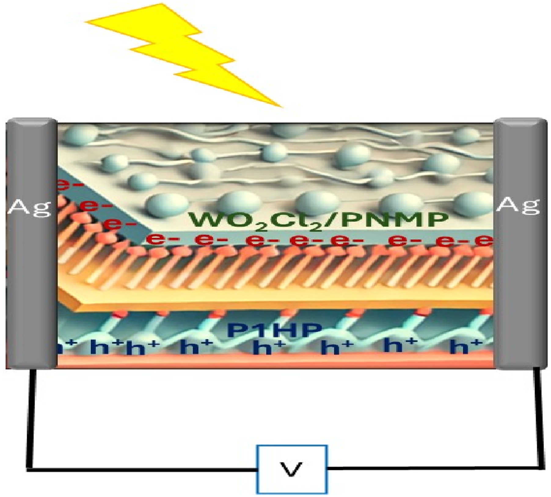

Results and discussion
Evaluation of the chemical, crystalline structure, and optical properties of WO2Cl2/PNMP cubic-composite
Transmittance measurements were used to investigate the optical properties of the WO2Cl2/PNMP cubic composite, as shown in Figure 2(a). The resulting FTIR transmittance spectrum displays several distinct absorption peaks at 664, 1400, 1618, 2379, and 3138 cm−1, which offer valuable insights into the material’s structural and chemical composition. Chemical, crystalline, and optical characterization of the WO2Cl2/PNMP cubic composite: (a) FTIR spectrum, (b) XRD pattern, and (c) optical analysis.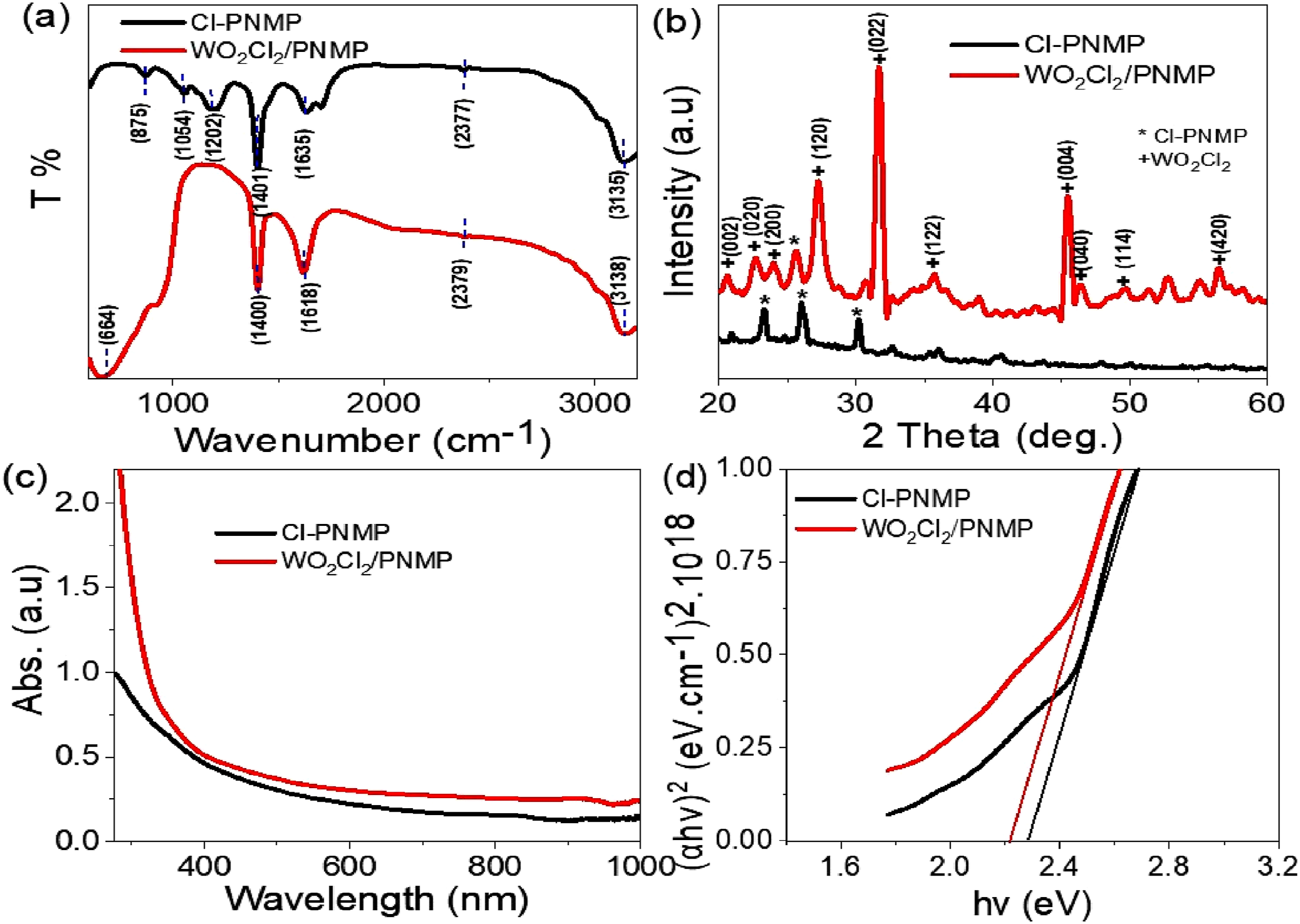
A notable red shift is observed in the nanocomposite at the absorption bands at 664, 1400, and 1618 cm−1 compared to the pristine PNMP. This red shift indicates alterations in the molecular environment due to incorporating WO2Cl2 into the PNMP matrix, resulting in changes in bond vibrations and intermolecular interactions. In contrast, a blue shift is noted for the peaks at 2379 and 3138 cm−1, suggesting a different molecular interaction at these higher wavenumbers, likely linked to modifications in hydrogen bonding or solvent coordination. 18 A particularly significant aspect of the transmittance spectrum is the emergence of a new peak at 664 cm−1, attributed to W–O stretching vibrations. This highlights the successful integration of tungsten-based species within the composite structure. The observed shifts in peak positions, paired with variations in peak intensities, further indicate a strong interaction between WO2Cl2 and PNMP, leading to changes in molecular vibrations and the composite’s overall optical behavior. The spectral changes observed provide compelling evidence for the effective incorporation of WO2Cl2 into the PNMP polymer network, forming a well-defined WO2Cl2/PNMP composite. These structural and optical changes imply improved material properties, positioning the composite as a promising candidate for advanced optical and electronic applications.
The structural and optical properties of synthesized materials are vital in their effectiveness across various applications, particularly optoelectronics. This study examined the crystalline behavior of the synthesized WO2Cl2/PNMP cubic-composite compared to the pristine Cl-PNMP structure. The analysis concentrated on the crystalline arrangement, peak intensity, and crystal size using XRD analysis. The results highlight how incorporating WO2Cl2 within the PNMP matrix improves the material’s overall crystallinity and optoelectronic performance.
The crystalline characteristics of the WO2Cl2/PNMP cubic composite were evaluated by analyzing the XRD pattern, as shown in Figure 2(b). The diffraction peaks in the XRD spectrum yield essential information about the material’s structural organization, including peak intensity, crystalline orientation, and grain size estimation. A notable increase in peak intensity was recorded following the integration of WO2Cl2 into the PNMP matrix, validating the successful incorporation of this inorganic phase into the polymeric framework.
For the inorganic WO2Cl2 component, 10 distinct diffraction peaks were observed at the following 2θ positions: 20.7°, 22.7°, 23.9°, 27.3°, 31.7°, 35.7°, 45.5°, 46.6°, 49.7°, and 56.6°. These peaks correspond to the Miller indices (002), (020), (200), (120), (022), (122), (004), (040), (114), and (420), indicating a well-ordered crystalline structure, JCPDS 830950. 19 These defined peaks imply the formation of a highly stable and crystalline material, vital for its electronic and optoelectronic properties. Conversely, the XRD pattern of pristine PNMP showed characteristic peaks in the 25.5° to 39.0° range, but with significantly lower intensity. This indicates that while PNMP has some crystallinity, its structural organization is relatively less robust than composite materials. The increased peak intensity in the WO2Cl2/PNMP cubic composite suggests that the dual oxidation process (using Na2WO4 and (NH4)2S2O8) has effectively enhanced the crystallization within the polymer matrix.
The crystalline size of the synthesized material was estimated from the XRD broadening of the diffraction peaks, notably at 27.3° and 31.7°. The average crystallite size measured was 11 nm, affirming the well-structured nanocrystals in the composite matrix. The analysis of Full Width at Half Maximum values was crucial for determining the crystallite size, as outlined in equation (3).20,21 The notable enhancement in crystalline behavior is essential in improving interactions between the material and incoming photons. Increased crystallinity results in superior electron mobility and energy absorption, rendering this composite material auspicious for optoelectronic and energy-harvesting applications.
A material’s ability to absorb and interact with photons is essential for its use in optical and electronic devices. The improved crystalline structure of WO2Cl2/PNMP significantly influences its photon absorption and energy transfer properties. When illuminated, the interaction between incoming photons and the composite’s active sites generates hot electrons. These high-energy electrons play a vital role in facilitating efficient energy transfer within the material, enhancing charge transport, and boosting the overall performance of optoelectronic devices.
The WO2Cl2/PNMP cubic-composite photon absorption characteristics were further assessed using UV- Vis spectroscopy, as shown in Figure 2(c). A comparison of the optical absorbance spectra between WO2 Cl2/PNMP and pristine PNMP showed a marked increase in absorbance following composite formation. Noteworthy findings from the optical characterization include a wider absorption range: The WO2Cl2/PNMP composite displayed strong absorbance across UV and visible regions, demonstrating its capability to interact effectively with a broad spectrum of photon energies. Additionally, there was an increase in absorbance intensity: The spectrum indicated a significant boost in intensity, implying a greater number of active sites available for photon interaction. Furthermore, the composite exhibited enhanced photon sensitivity, positioning it as a favorable option for photodetectors and solar energy applications. This optical improvement is attributed to the addition of WO2Cl2, which introduces extra electronic states within the composite structure. These states facilitate better photon excitation, charge separation, and electron transport, thus enhancing the overall efficiency of the material in optoelectronic applications. With its superior crystallinity, improved photon absorption, and efficient charge transport, the WO2Cl2/PNMP cubic-composite offers significant promise for advanced applications. Figure 2(d) reveals that the calculated bandgap for the composite rises to 2.1 eV, compared to the Cl- PNMP bandgap of 2.2.3 eV. These values are determined using the Tauc equation, which utilizes the absorbance coefficient (α) derived from the absorption (A) as per equation (4).22,23


The oxidation states of the main elements in the WO2Cl2/PNMP cubic composite, especially tungsten (W), and related elements have been determined using XPS analysis. This technique is vital for understanding the composite’s structural composition and effectively supports findings from XRD analysis. Figure 3(b) analyzes explicitly the oxidation state of tungsten, a crucial component of the composite. The XPS spectra indicate that tungsten predominantly exists in the +6 oxidation state, as shown by the distinct binding energies of the W4f7/2 and W4f5/2 peaks at 35.8 eV and 37.9 eV, respectively.
24
These measurements correspond well with the standard binding energy range for W(VI), thereby confirming its oxidation state in the composite matrix. Additionally, the oxygen (O) and chlorine (Cl) within the WO2Cl2 structure are analyzed through their core-level binding energy transitions. The oxygen 1s peak appears at 530.8 eV, as shown in Figure 3(c), indicating its role in the tungsten oxide framework. Likewise, the chlorine 2p transition is observed at 199.2 eV, illustrated in Figure 3(d), confirming chlorine’s role in the composite structure. Figure 3(a) presents a comprehensive elemental survey that shows carbon (C) and nitrogen (N) contributions from the PNMP polymeric matrix. These organic elements are vital for defining the composite framework, aiding stability, and functionalization. Concurrently, the spectral features of W, O, and Cl affirm the successful integration of the inorganic WO2Cl2 phase within the PNMP structure. The XPS results are key to clarifying the composite’s electronic environment and chemical interactions. They reveal a clearly defined distribution of oxidation states, reinforcing the structural integrity and composition of WO2Cl2/PNMP. Furthermore, the complementary use of XPS and XRD techniques offers a more comprehensive understanding of the composite’s crystallographic and electronic properties. This thorough investigation enhances the material’s prospects for various advanced applications, especially in catalysis, electronic devices, and energy storage systems, where fine control over oxidation states and element integration is essential for optimizing performance. (a) The total survey of WO2Cl2/PNMP cubic composite, (b) W, (c) O, and (d) Cl elements.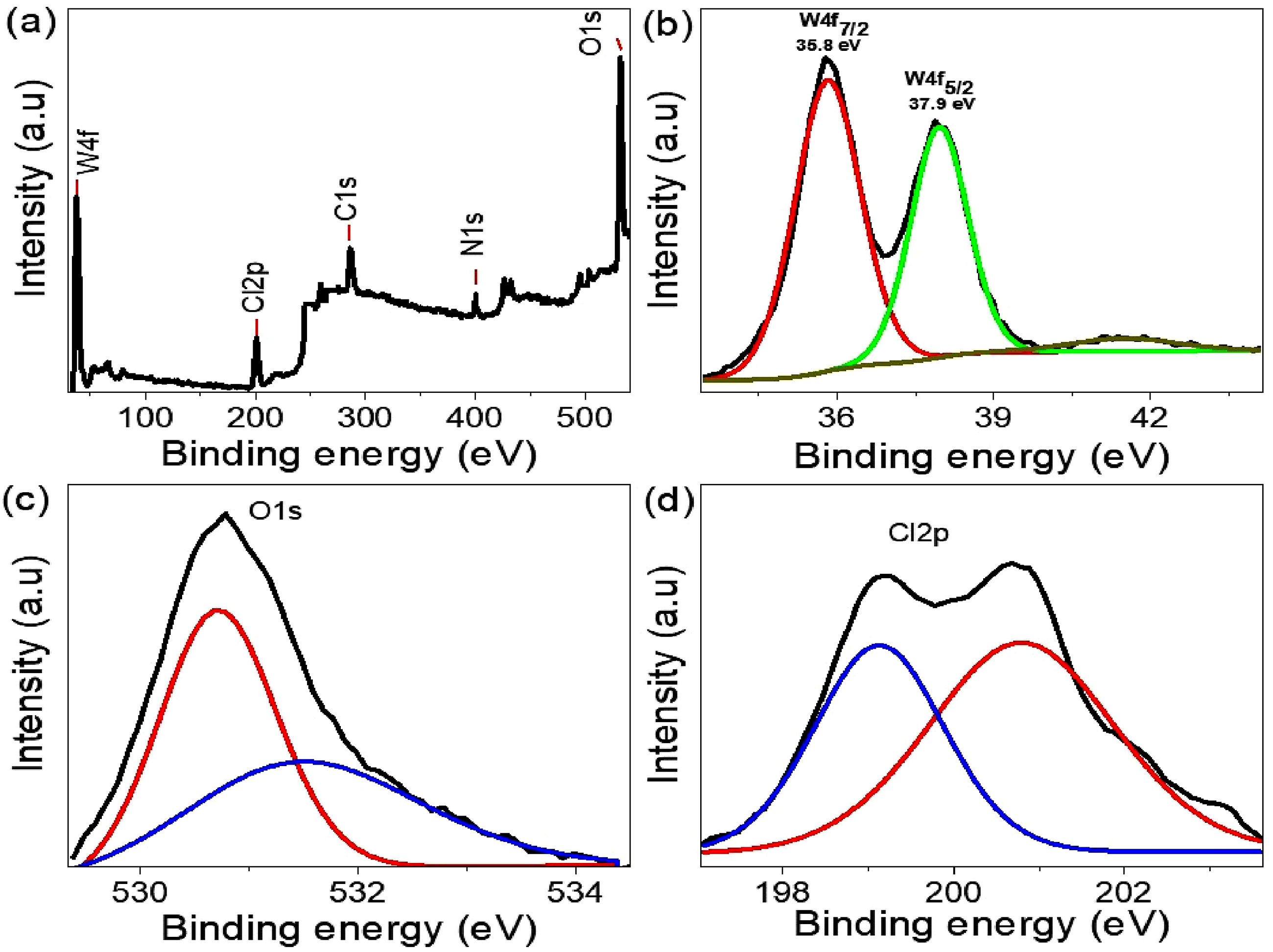
Figure 4 presents a comprehensive morphological analysis of the WO2Cl2/PNMP cubic composite, conducted through SEM and TEM observations at various magnifications. It also contrasts the pristine PNMP polymer to highlight structural modifications from adding WO2Cl2 nanostructures. Figure 4 (a) and (b), the SEM images at differing magnifications reveal the distinctive cubic shape of the WO2Cl2/PNMP composite. These uniformly arranged cubic structures indicate a controlled synthesis process that ensures consistent material formation. A closer inspection of panel (b) uncovers the complex surface texture of the cubic particles, densely coated with nanoscale features. These characteristics contribute to increased surface roughness, with the particle size estimated to be approximately 11 nm. This morphological improvement greatly enhances optoelectronic applications by facilitating better light absorption, charge separation, and charge transport.
25
Figure 4 (c) and (d) present TEM images that provide greater insights into the nanoscale structure of the WO2Cl2/PNMP composite. In Figure 4(c), uniformly distributed nanoscale domains are visible, with particle sizes between 11.49 and 17.76 nm. These nanoscale characteristics enhance the composite’s optoelectronic properties by promoting efficient charge carrier separation and transport. Figure 4(d) features a high-resolution TEM image that reveals distinct lattice fringes with an interplanar distance of 0.8 nm. This observation confirms the crystalline nature of the WO2Cl2 phase within the composite, which is crucial for enhancing charge mobility and minimizing recombination losses. The organized crystalline structure supports efficient electron transport, making this material well-suited for high-performance optoelectronic applications. In contrast, Figure 4(e) and (f) showcase the SEM characterization of the pristine PNMP polymer under different magnifications. Unlike the clearly cubic morphology seen in the composite, the pristine PNMP exhibits a highly porous and irregularly aggregated structure with loosely packed nanoparticles, approximately 120 nm in diameter. This chaotic morphology significantly contrasts with the structured cubic formations of the WO2Cl2/PNMP composite. The inclusion of WO2Cl2 into the polymer matrix markedly modifies the material’s morphology, enhancing its structural integrity and electronic properties. This change highlights the cooperative interaction between WO2Cl2 nanostructures and the PNMP polymer, leading to improved optoelectronic performance. The composite’s well-ordered architecture supports effective charge transport and enhanced light absorption, making it a highly promising candidate for advanced photodetectors and energy-harvesting technologies.26,27 Morphological characteristics of the WO2Cl2/PNMP cubic composite: (a and b) SEM images at different magnifications, (c and d) TEM images at varying magnifications, and (e and f) SEM images at different magnifications of the pristine PNMP.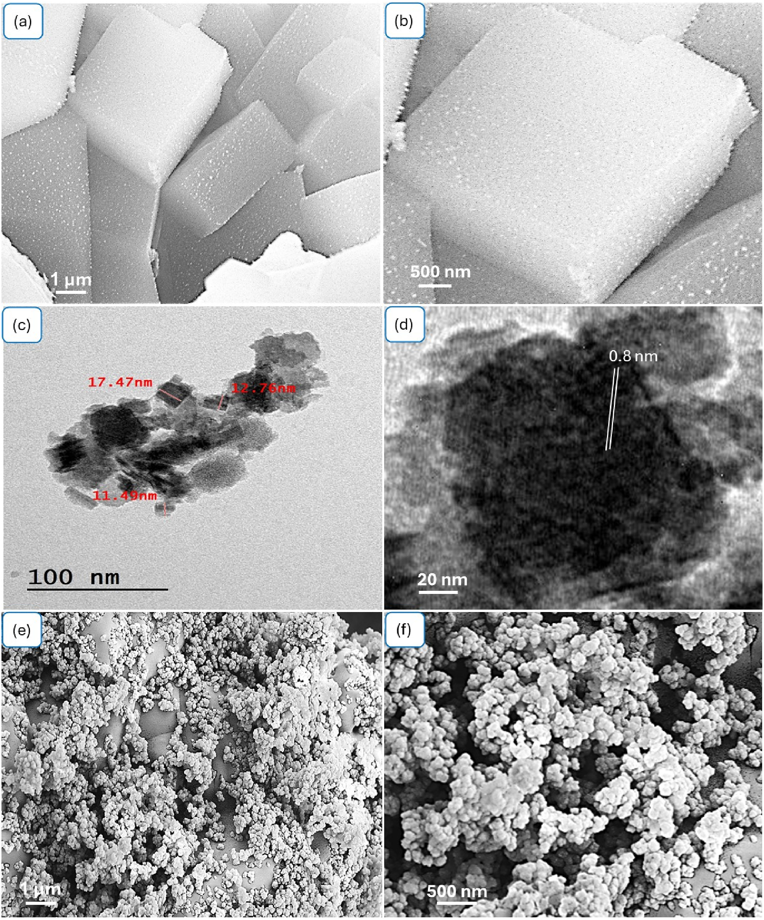
The EDX spectrum of the WO2Cl2/PNMP cubic composite confirms the presence of the main constituent elements. The strong peaks of tungsten (W) at ∼1.8 and 8.4 keV validate the incorporation of WO2Cl2. A sharp Cl signal around 2.6 keV supports the oxychloride structure. O and N peaks indicate the contribution of PNMP polymer, while C reflects the organic polymer backbone. Na may originate from residual precursors or processing steps. The elemental composition demonstrates the successful hybridization of the inorganic WO2Cl2 component with the polymeric PNMP matrix, confirming the formation of the designed cubic composite.
Electrical testing of the fabricated WO2Cl2/PNMP/P1HP optoelectronic device
The electrical characteristics of the optoelectronic device, constructed with the WO2Cl2/PNMP/P1HP layers, were comprehensively assessed through various electrical tests. The thin-film device was linked to a CHI workstation via an electrical circuit, ensuring precise electrical properties were measured. Silver (Ag) paste was applied at both ends of the device to create this connection, establishing effective contact points for accurate transmission of electrical signals. This arrangement facilitated a comprehensive evaluation of the composite’s charge carrier dynamics and photocurrent response under different light conditions. 28
The fundamental concept underlying the electrical characterization of this semiconductor device focuses on examining the hot electron generation mechanism. When an external potential is applied, the WO2Cl2/PNMP/P1HP semiconducting properties produce an internal electric field. This electric field is essential for directing the movement of excited charge carriers, specifically urging hot electrons towards the device’s external surface, which generates a measurable photocurrent density (Jph). The efficiency of this mechanism is directly linked to the composite material’s optoelectronic performance, as it influences the material’s capability to capture and convert incoming light into electrical energy.
Figure 5 illustrates the recorded Jph values over a potential range from −2. 0 V to +2. 0 V. The findings indicate a notable increase in photocurrent generation under light illumination compared to dark conditions. In particular, when exposed to light, the device reached a peak photocurrent density of about 0. 39 mA cm−2, while in darkness, the WO2Cl2/PNMP/P1HP intrinsic semiconductor properties resulted in a lower dark current (Jo) of 0. 22 mA cm−2. This significant contrast between light and dark current values emphasizes the composite’s strong optoelectronic response, affirming its capability as an effective photoactive material. Photoelectrical performance of the WO2Cl2/PNMP/P1HP optoelectronic device. (a) J-V characteristics under dark (black) and light (red) conditions, demonstrating the enhanced photocurrent generation upon illumination. (b) Reproducibility of the device performance over multiple light exposure runs, confirming its stability and reliability.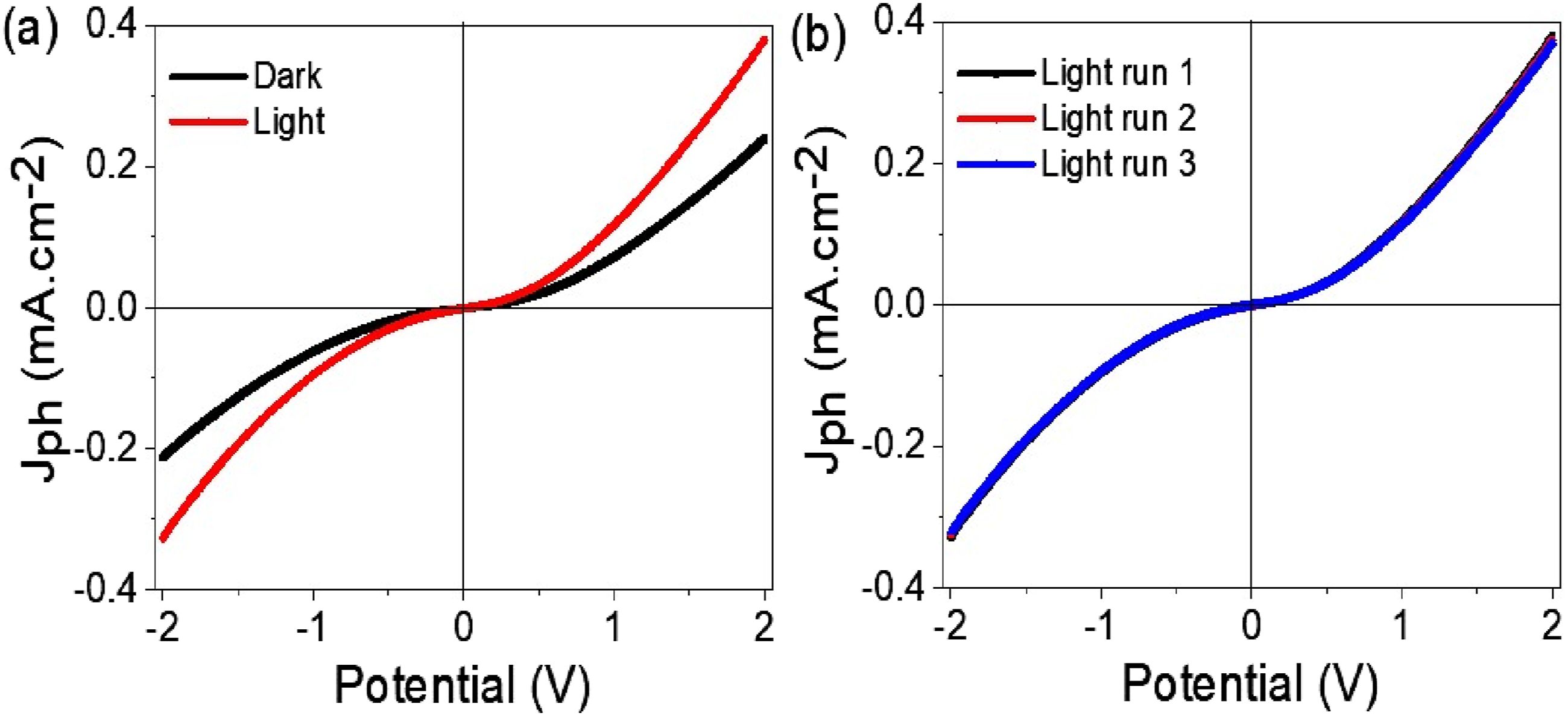
The substantial increase in photocurrent observed under illumination can be linked to the WO2Cl2/PNMP/P1HP semiconducting attributes, which enable efficient photon absorption. When exposed to light, the material experiences photon excitation, activating charge carriers within its structure. This leads to the generation of hot electrons, which are then propelled by the internal electric field, enhancing charge separation and improving carrier transport.29,30 The composite’s excellent charge transport properties further enhance its photocurrent response, positioning it as a promising candidate for various optoelectronic applications, including photodetectors and solar energy harvesting devices.
Additionally, the stability of the optoelectronic device was evaluated through several test runs, as shown in Figure 5(b). Repeated measurements’ nearly identical Jph curves demonstrate the WO2Cl2/PNMP composite’s high stability and reproducibility. This suggests that the material retains its optoelectronic performance across multiple cycles, making it a dependable option for long-term sustainable energy and electronic applications. The combination of substantial photocurrent generation, outstanding charge carrier mobility, and exceptional stability highlights the potential of this composite material for next-generation optoelectronic device technologies. The photodiode Schottky behavior observed in this curve indicates the device’s strong potential for light response, suggesting a preference for Schottky over Ohmic behavior.
Figure 6(a) reveals essential insights into the high sensitivity and optoelectronic capabilities of the WO2Cl2/PNMP/P1HP device. This is demonstrated by analyzing the relationship between the Jph and the applied potential under different photon energies during illumination. Utilizing photons with varying energy levels allows for assessing how well the composite absorbs and converts incoming light into electrical energy. Since different photon energies align with specific effective wavelengths, the surface’s response to these photons offers essential information regarding the material’s optoelectronic characteristics, as illustrated in Figure 6. The composite’s optoelectronic performance was assessed using photon energies of 1.7 eV, 2.3 eV, 2.8 eV, and 3.6 eV, showing differences in the generated photocurrent density. At higher photon energies like 3.6 eV and 2.8 eV, the composite shows a marked photocurrent response, with values of 0.34 mA cm−2 and 0.33 mA cm−2, respectively. This strong response indicates that the material effectively absorbs light in the spectrum’s ultraviolet (UV) and visible ranges. The increased photocurrent generation at these energy levels likely results from the optimized band structure and excellent charge transfer properties of the WO2Cl2/PNMP/P1HP layers. (a) Current density versus potential for the WO2Cl2/PNMP/P1HP device under different photon energies (1.7 eV, 2.3 eV, 2.8 eV, and 3.6 eV), demonstrating the material’s sensitivity to incident light and its efficient charge transfer properties. (b) The maximum Jph values as a function of photon energy at 2.0 V.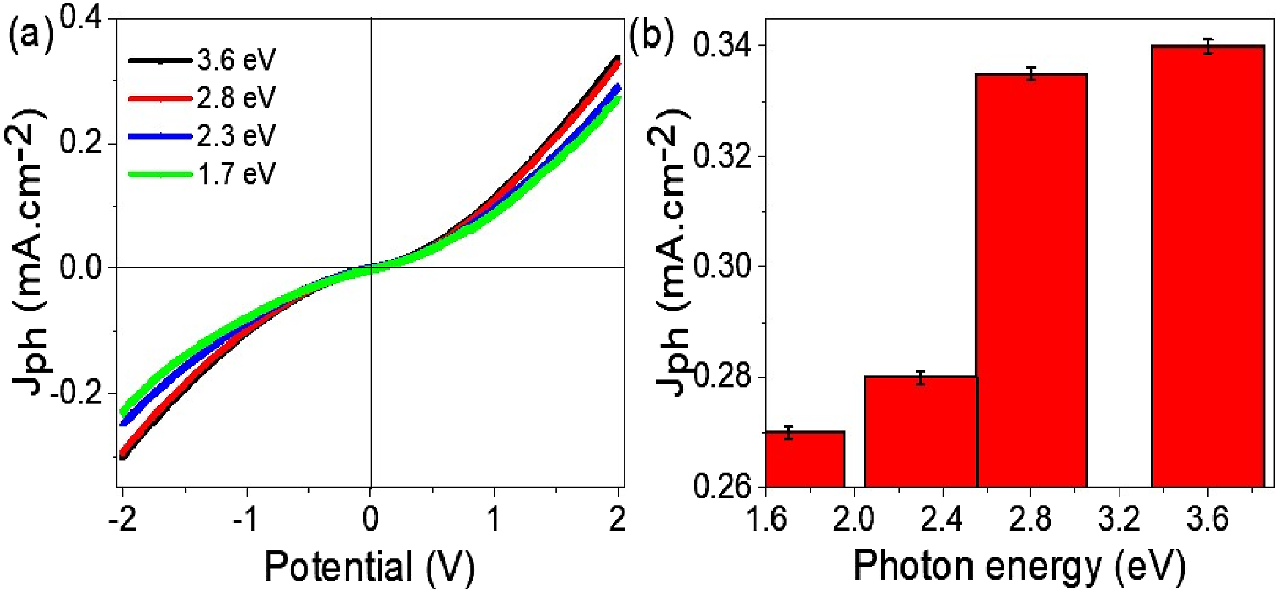
In contrast, the photocurrent density significantly declines at lower photon energies, specifically those under 2.8 eV. At 2.3 eV and 1.7 eV, the measured photocurrent values are 0.28 mA cm−2 and 0.27 mA cm−2, respectively. These measurements reveal that while the composite still allows charge transfer at these lower photon energies, its efficiency is notably less than that of higher-energy photons. This pattern indicates that the material’s band structure allows absorption and electron excitation at lower energies but with reduced effectiveness. A more detailed comparison of Jph values as a function of photon energy is illustrated in Figure 6(b). The WO2Cl2/PNMP/P1HP performance can be credited to the distinct electronic properties of its components. WO2Cl2, a transition metal oxyhalide, shows strong optical absorption across both visible and UV spectra. This feature facilitates efficient electron excitation, rendering the material highly appropriate for light-harvesting. Furthermore, PNMP, a conjugated polymer, is vital in enhancing charge transport by minimizing electron-hole recombination, thus contributing to the improved photocurrent response noted at higher photon energies.31,32
The upward trend in Jph with increasing photon energy indicates that the composite material likely has an approximate bandgap of 2.3 eV, making it especially effective for applications driven by visible light. Additionally, the observed photocurrent saturation beyond 2.8 eV signifies that further increases in photon energy do not substantially boost charge carrier generation past a certain threshold. This behavior suggests that the material attains its peak charge carrier excitation efficiency within the range of 2.8–3.6 eV, positioning it as a strong candidate for use in photodetectors, photovoltaic cells, and photocatalytic systems.
Figure 7(a) and (b) provide an in-depth analysis of the photoresponsivity (R) and detectivity (D) of the WO2Cl2/PNMP/P1HP device, highlighting its promise as a high-performance material for optoelectronic applications. The R value assessment across various optical regions showcases the composite’s effectiveness in transforming incident photons into an electrical signal. The graph in Figure 7(a) reveals a significant rise in R as photon energy increases from 1.6 eV to 3.6 eV, peaking at about 3.4 mA·W−1 at elevated energies. This trend emphasizes the composite’s efficiency in generating charge carriers through photon absorption, especially in the visible and near-ultraviolet (UV) regions. The improved responsivity results from the robust interaction between WO2Cl2 nanostructures and the PNMP polymer matrix, which aids in effective charge separation and reduces recombination losses. These attributes position this composite as an excellent choice for optoelectronic applications, including photodetectors and solar energy harvesting devices, where a broad optical absorption range is vital for enhanced performance. The optoelectronic properties of the WO2Cl2/PNMP/P1HP device, showing (a) the photoresponsivity (R) as a function of photon energy, demonstrating an increasing trend with higher photon energies, and (b) the detectivity (D) as a function of photon energy, indicating enhanced sensitivity to weak optical signals, particularly in the UV-Vis range.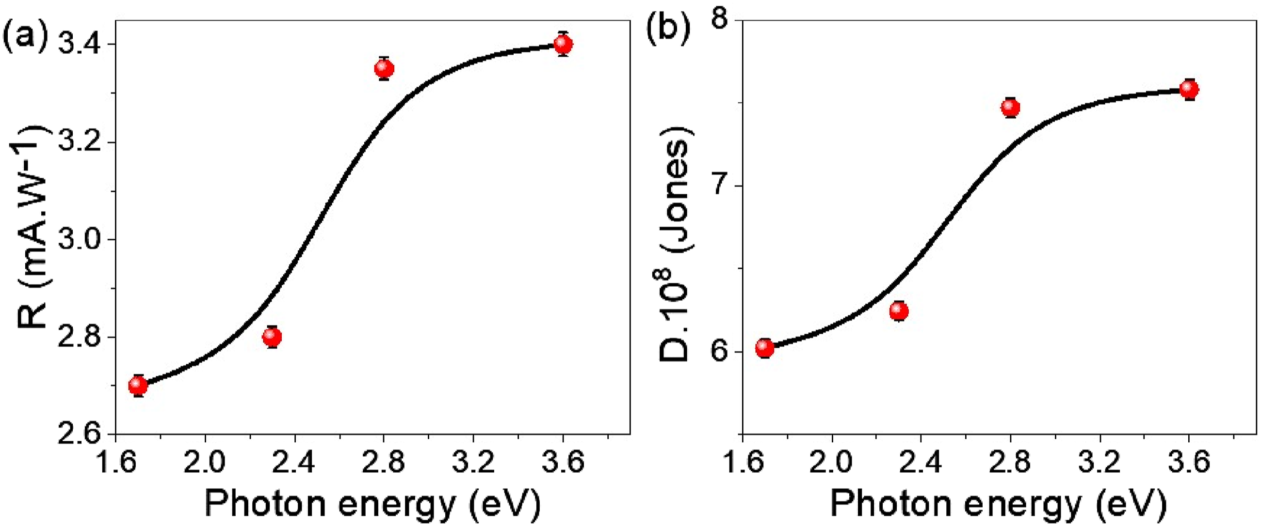
Figure 7(b) depicts the detectivity (D), measured in Jones (cm·Hz1/2 W−1), indicating the material’s capacity to detect faint optical signals while limiting noise interference. The detectivity of the WO2Cl2/PNMP/P1HP device significantly increases with higher photon energy, peaking at around 0.75 × 10⁹ Jones at 3.6 eV. This improvement reflects a low dark current, a crucial element for achieving high signal-to-noise ratios in optoelectronic applications. Additionally, the composite shows enhanced photogenerated carrier mobility, ensuring a strong photocurrent response even under low-light conditions. This characteristic renders the composite well-suited for low-light detection, making it an ideal material for high-sensitivity photodetectors in visible and UV spectral regions.
The encouraging findings from these analyses reveal several significant benefits of the WO2Cl2/PNMP/P1HP device. Firstly, this material shows a broad optical response, with strong responsivity and detectivity across a wide range of photon energies, making it an adaptable choice for broadband photodetection. Secondly, the composite’s enhanced charge transport properties arise from the synergistic interaction between WO2Cl2 nanostructures and PNMP polymer chains, which results in improved electron mobility, reduced carrier recombination, and higher overall device efficiency. Moreover, the material’s high sensitivity and stability guarantee reliable performance even in low light conditions, which is crucial for applications like night vision sensors, biomedical imaging, and optical communication systems. Lastly, the combination of high responsivity and detectivity indicates that WO2Cl2/PNMP/P1HP device photodetectors could outperform conventional semiconductor-based devices, particularly in ultraviolet-visible (UV-Vis) photodetection and energy-harvesting technologies. These characteristics make the WO2Cl2/PNMP/P1HP device a highly promising material for next-generation optoelectronic devices.
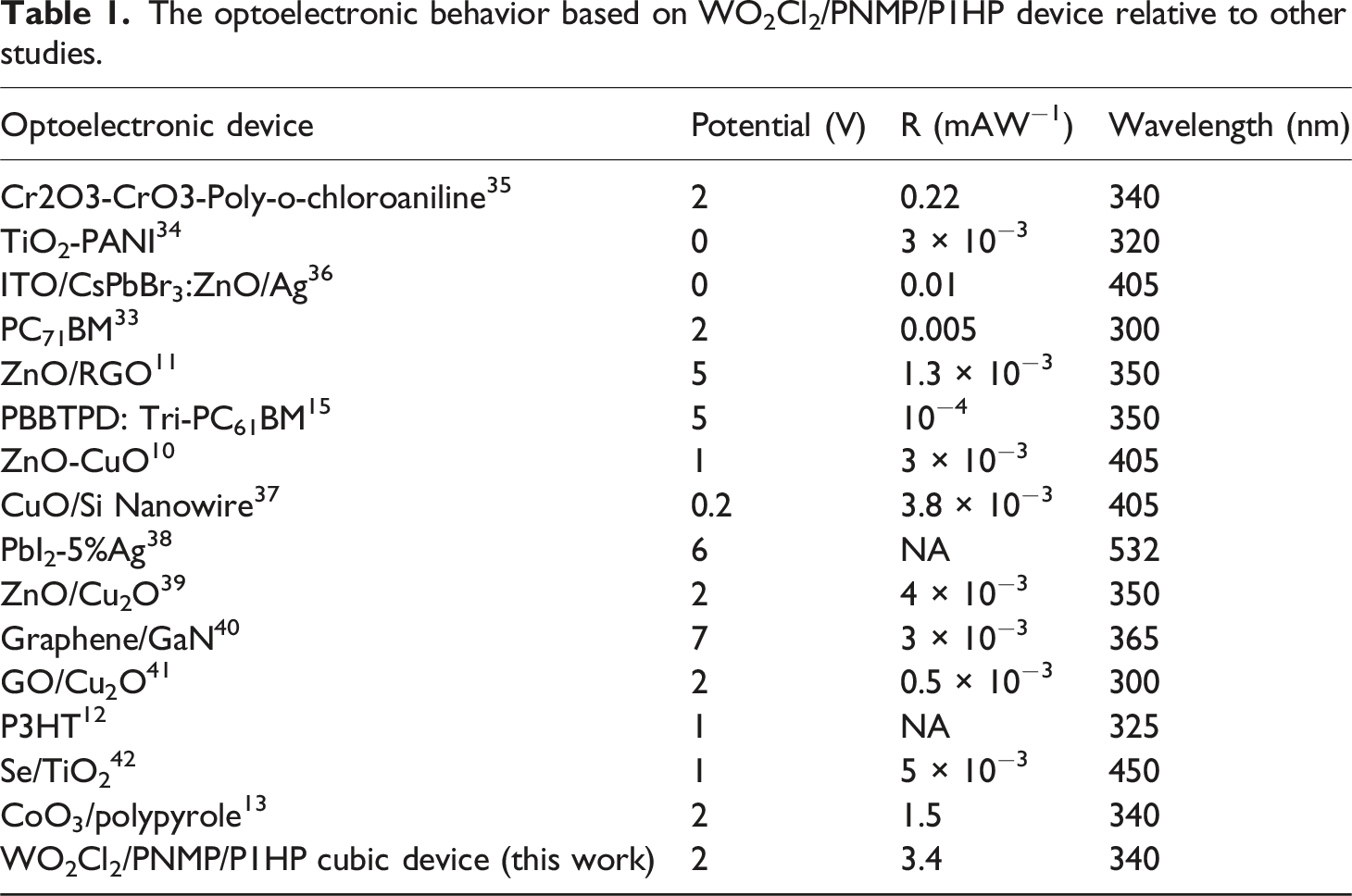
The optoelectronic behavior based on WO2Cl2/PNMP/P1HP device relative to other studies.
Conclusions
A one-pot fabrication method has successfully created a high-performance optoelectronic device utilizing WO2Cl2/PNMP/P1HP layers. This composite’s structural and chemical composition was thoroughly analyzed using XRD and XPS techniques. The XRD results revealed intense diffraction peaks, signifying a crystallite size of around 11 nm, while the XPS analysis confirmed the presence of tungsten (W) in the +6 oxidation state. This well-defined crystalline structure and oxidation state enhance the optical properties of the material, particularly in visible and ultraviolet ranges. The WO2Cl2/PNMP/P1HP-based optoelectronic device displayed impressive Jph values across varying photon energies. At 3.6 eV, the device achieved a Jph of 0.34 mA cm−2, with a Jph of 0.28 mA cm−2 at 2.3 eV. These findings underscore the material’s effective photoconductive response, which is essential for advanced optoelectronic use. The device exhibited an optimized photoresponsivity (R) of 3.4 mA·W−1 at 3.6 eV, highlighting its strong light-harvesting capabilities. The estimated D value of 0.75 × 10⁹ Jones at this photon energy emphasizes its high-sensitivity photodetection potential. Beyond exceptional technical performance, this optoelectronic thin film is also economically viable for cost-effective mass production, establishing it as a prime contender for industrial applications. With remarkable optoelectronic characteristics, structural stability, and scalability, the WO2Cl2/PNMP/P1HP device stands out as a promising material for photodetectors, optical sensors, and other next-generation light-responsive technologies.
Supplemental Material
Supplemental Material - Optimal cubic composite of tungsten (VI) oxide chloride/poly N-methyl pyrrole as a potential thin film for optoelectronic uses with the photodiode behavior
Supplemental Material for Optimal cubic composite of tungsten (VI) oxide chloride/poly N-methyl pyrrole as a potential thin film for optoelectronic uses with the photodiode behavior by Amira Ben Gouider Trabelsi, Fatemah H. Alkallas, and Mohamed Rabia in Journal of Thermoplastic Composite Materials.
Footnotes
Acknowledgements
The authors extend their appreciation to the Deanship of Scientific Research and Libraries in Princess Nourah bint Abdulrahman University for funding this research work through the Research Group project, Grant No. (RG-1445-0010).
Author contributions
Amira: Writing assistance, data analysis, and revising the manuscript.
Fatemah: Workflow management, funding, and supervision.
Mohamed: Experiments, analysis, and writing.
Declaration of conflicting interests
The author(s) declared no potential conflicts of interest with respect to the research, authorship, and/or publication of this article.
Funding
This research was funded by the Deanship of Scientific Research and Libraries in Princess Nourah bint Abdulrahman University for funding this research work through the Research Group project, Grant No. (RG-1445-0010).
Data Availability Statement
All data generated or analysed during this study are included in this article.
Supplemental Material
Supplemental material for this article is available online.
References
Supplementary Material
Please find the following supplemental material available below.
For Open Access articles published under a Creative Commons License, all supplemental material carries the same license as the article it is associated with.
For non-Open Access articles published, all supplemental material carries a non-exclusive license, and permission requests for re-use of supplemental material or any part of supplemental material shall be sent directly to the copyright owner as specified in the copyright notice associated with the article.