
Abstract
Polymer/graphene nanocomposites (PGNs) have shown great potential as dielectric and energy storage materials. However, insolubility of graphene in most solvents, hydrophobic behaviour and poor dispersion in polymer matrix restrict wider fabrications and applications of PGNs. In this study, we present co-fabricated PGNs engineered by solution blending and melt compounding methods with improved dielectric performance. Further processing of PGNs by melt mixing after solution blending not only improved dispersion of graphene in the matrix but also ensured good interfacial interaction of the composites’ constituents and reduction of oxygen content in PGNs. Graphene nanoplatelets used in this study was slightly functionalized (fGNPs) to enhance dispersion in the polymer matrix. It was later characterized using Fourier transform infrared (FTIR) and Raman spectrometer. Scanning electron microscope (SEM) was used in morphological study of the fabricated composites. Dielectric properties, electrical conductivity, breakdown strength and energy storage capacity of the fabricated composites were investigated. The results obtained showed well-dispersed fGNPs in poly (vinylidene fluoride) (PVDF) matrix and improved dielectric performance. For instance, with 3.34 wt% and 6.67 wt% fGNPs co-fabricated composites, dielectric constant increased from about 9 for neat PVDF to 9930 and 38,418 at 100 Hz, respectively. While 7588 and 12,046 were respectively measured for solution blended-only composites at similar fGNPs content. These resulted to about 176.9% and 376.4% increase in energy storage density with 3.34 wt% and 6.67 wt% fGNPs co-fabricated composites when compared to their counterparts. These results were also credited to strong bonding, reduction of oxygen and recovered graphene structure by melt-mixing approach.
Introduction
Polymeric materials have found wide applications in engineering and non-engineering sectors such as polymer textile, electrical and electronic industries, food packaging technology and biomedical, mechanical and structural components. These broad applications are due to their various desired properties such as lightweight, chemical resistance and easy processing. Polymers and their composites are also used in the fabrication of electrochemical and electrostatic capacitors (ESCs) for energy storage, power conditioning, correction factor, signal processing, decoupling and so on. In energy storage technologies, ESCs are desired due to their fast charging and discharging capability, resulting from their high power density. 1 However, they are characterized with low energy density, 2 which has limited their application in designing high energy storage devices. This can be attributed to their low dielectric constants, usually below 10. 3
There is increasing demand for high dielectric constant materials for next-generation electronic devices and high energy storage density dielectric materials. It has been noted that single dielectric materials such as polymers or ceramics cannot give dielectric performance required for next-generation capacitor applications such as small layout area material with high dielectric constant. 4 This has led materials researchers in combination with various materials in search of high dielectric constant materials. Currently, polymer/graphene nanocomposites (PGNs) have shown promising potential as high dielectric constant materials. 5 The high dielectric constant of PGNs is creditable to good properties of polymeric materials in conjunction with excellent properties of graphene such as good mechanical, thermal and electrical properties. 6,7 Graphene is a 2D and high aspect ratio material with carbon atoms in sp2 bonds and honeycomb crystal structure. 8 The unique properties of graphene made it a potential material in energy-related fields such as hydrogen storage, batteries, capacitors and fuel cells. 9 Generally, graphene-based composite materials have attracted broad applications interest due to their desired electronic, electrical, optical, magnetic, chemical, catalytic, biomedical and sensing properties. 10 –12
Notwithstanding reported increase in dielectric constant of PGNs due to the formation of mini-capacitors in polymer matrix, 13,14 their practical applications as ESCs and energy storage materials are hindered. The limited applications of PGNs as ESC are due to high energy dissipation, high dielectric loss and low voltage endurance resulting from high current leakage. 1,15,16 Poor dispersion of graphene and interfacial interaction with polymer matrix are also challenges restricting excellence fabrications and broad applications of PGNs. 17 Therefore, various fabrication techniques have been used in the preparation of PGNs. For instance, Jinhong et al., 18 Li et al., 19 Chiu and Chen, 20 Wu et al. 21 and Maity et al. 22 synthesized PGNs by solution blending and reported improved properties as related to their various objectives and findings. According to Zhang et al., 17 good dispersion of graphene can be achieved by solution blending. However, solution blending has high tendency of re-clustering or settling of graphene sheets in polymer matrix during recovering of PGNs from solution, especially by evaporation technique. 16 Hence, it may result in poor and undesired properties such as low dielectric constant and high energy dissipation.
Many reports have shown that modification or oxidation of graphene sheets enhances their dispersion in the polymer matrix with improved properties. For instance, Wang et al., 23 Xu et al., 24 Wang et al. 25 and Maity et al. 26 reported improved dielectric and electrical properties of polymers incorporated with modified graphene. Modification of graphene sheets destroys their conjugal structures, introduces sp3 defects domain and deteriorates their excellent thermal, mechanical and electrical properties. 27 In that regard, graphene structure recovery after modification became necessary for effective performance. Various authors have used chemical 13,28 and thermal 15,29 means in recovering graphene structure after modification, which can also be beneficial for other purposes. For instance, Zhao et al. 30 demonstrated that reaction of graphene oxide (GO) with phenol can both act as oxygen removal from GO and guide on its surface for in situ polymerization. However, chemical reduction of GO can also increase sp3 defect sites during reaction. 31 While long-time exposure of PGNs at elevated temperature as in the case of most reported in situ thermal reduction can lead to thermal degradation.
According to Uyor et al., 16 melt compounding can provide well distribution of graphene sheets in the polymer matrix by mechanical mixing at high temperature and shear forces, which enables effective entangling and intercalation of polymer molecular chains with graphene sheets. In this study, we took advantages of both solution blending and melt compounding in the fabrication of PGNs. These routes ensured homogeneous dispersion of graphene and strong interfacial interaction with the polymer matrix. The co-fabrication approach also ensured recovery of graphene structure and reduction of oxygen-containing functional groups in short-time in situ thermal reduction. These were practically possible due to direct contact of functionalized graphene nanoplatelets (fGNPs) with hot walls and rotating screw of the melt compounding device used. On the other hand, slight functionalization of GNPs led to only little introduction of sp3 domain within their sp2 network configuration. Therefore, the two-way fabricated PGNs showed better dielectric performance and energy storage capacity compared to single-way fabricated PGNs. This study revealed that the co-fabrication approach is a prospective route to achieve PGNs with reduced oxidized graphene without the use of chemicals and homogeneously dispersed graphene in the polymer matrix. To the best of our knowledge, no work has been presented on such dual fabrication approach in the study of dielectric performance and energy storage capacity of PGNs. The fabricated composites are expected to find applications as capacitor materials and other related engineering applications.
Experimental section
Materials
Slightly oxidized GNPs (carbon >95 wt%, oxygen <3 wt%, surface area of 110 m2 g−1, diameter 2–3 μm, thickness 6–8 nm average), poly (vinylidene fluoride) (PVDF) powder (average molecular weight approximately equal to 534,000 and density is 1.74 g mL−1 at 25°C), 3-hydroxytyramine hydrobromide (HTHB; assay 99%, MP 218–220°C), N,N-dimethyl formamide (DMF) (assay ≥ 99%) were all sourced from Sigma-Aldrich (South Africa). Ammonia solution (25%) was purchased from Thembane Chemicals (South Africa).
Functionalization of GNPs
Functionalization of GNPs was done with HTHB as shown in Figure 1. Typically, 100 mg of GNPs was dispersed in 100 mL of distilled water in a beaker. Ultrasonication was applied for 1 h to exfoliate GNPs. Then, 80 mg of HTHB was added to the mixture with slow addition of 2 mL of ammonia solution to activate the reaction. Simultaneous ultrasonication and mechanical stirring at 80°C was applied for 6 h to obtain fGNPs. After the reaction, a dark solution was obtained, and the particles showed hydrophilic behaviour. The solution was filtered with 0.22-μm pore size filter membrane and was later washed with distilled water and DMF till the solution turned clear. Part of the fGNPs was dried in an air circuiting oven overnight for characterizations, while some were dispersed in DMF prior to use.
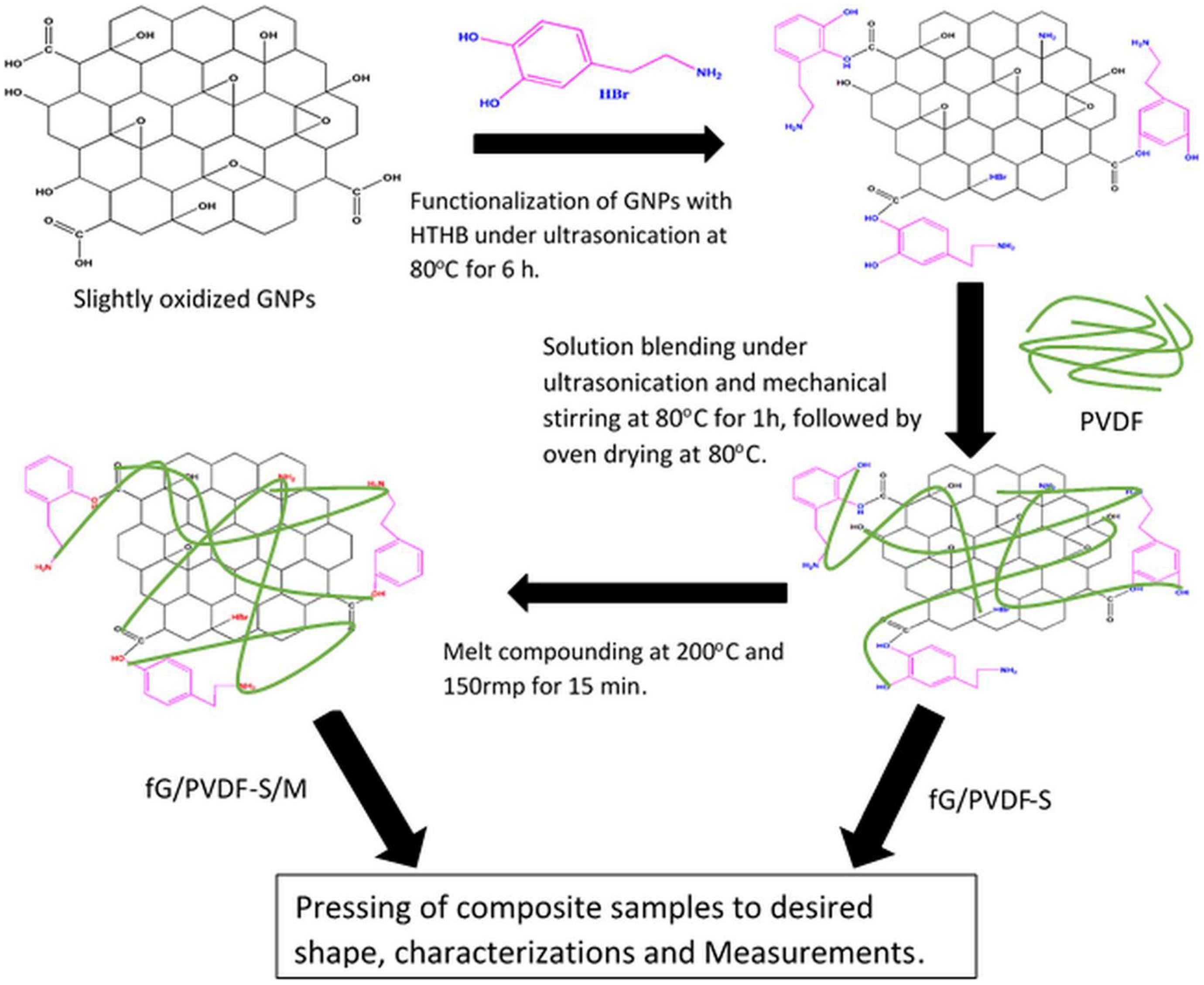
Schematic representation of GNPs functionalization and composites fabrication routes.
Preparation of composites
The composites preparation followed the routes as illustrated in Figure 1. PVDF powder was dissolved in DMF under magnetic stirring at 60°C for 10 min. Then desired amount of pre-dispersed fGNPs was added to it. The mixture was kept under ultrasonication and mechanical stirring for 1 h at 80°C. The composites were cast on clean glass substrates and were later dried in an air circulating oven at 80°C till the weight became constant. The composite films were grinded, then melt-compounded using HAAKE Rheomix 600 OS (Thermo Scientific, United States) at 200°C and 150 rpm for 15 min. Finally, the composites were pressed to flat shape of about 0.03 cm thickness using carver press moulder at 200°C and 10 MPa for 5 min. The samples were denoted as xfG/PVDF-S/M, where x is the weight percentage concentration of fGNPs and S and M represent solution blended and melt compounded composites. Also, solution blended-only composites were prepared for comparison and was denoted as xfG/PVDF-S. The concentration of fGNPs in PVDF matrix was varied from 1.67 wt% to 6.67 wt%.
Characterizations and measurements
Successful functionalization of GNPs was investigated using Fourier transform infrared (FTIR) spectrometer (Perkin Elmer spectrum 100, Perkin Elmer Inc, United States). An attenuated total reflection mode was used and was measured in the range of 1000–2500 cm−1 wave number. Raman spectrometer (LABRAM-HR, Horiba Ltd, Japan) was used to examine the level of GNPs’ structural destruction after functionalization. The spectrometer has excitation wavelength source of 414.5-nm laser. The investigation was carried in the range of 1000 cm−1 to 2000 cm−1 Raman shift. Morphology of the composite samples were studied using high-performance scanning electron microscope (SEM; VEGA 3 TESCAN, Czech Republic) at an accelerated voltage of 20 kV. Fractured surfaces of the samples were coated with conductive carbon before viewing under the SEM. Energy-dispersive spectrometer (EDS) analysis was also conducted. Capacitance (C (F)) and resistance (R (Ω)) of the samples were measured using LCR meter (B&K 891, B&K Precision, United States) over the frequency range of 100 Hz to 100 KHz. The composite films were coated with silver paste to avoid contact resistance. ESCs were designed by inserting the composite films between parallel copper plates of 1.7 × 1.5 cm2 dimension. The sides of the ESCs were coated with epoxy resin to avoid current leakage. Dielectric constant (ε′), dielectric loss (ε″), electrical conductivity (δ (Ωm)−1), energy storage density (Ub (J m−3)) and polarization (P (C m−2)) of the samples were calculated using equations (1), (2), (3), (4) and (5), respectively. Breakdown strength (E (V m−1)) of the composite films were determined using Conelectric high voltage transformer (BS 3941, South Africa). The composite films were placed between two ball copper electrodes. Voltage was gradually increased till a pop sound was heard. The voltages at which this occurred were recorded as the breakdown voltage of the composite films.
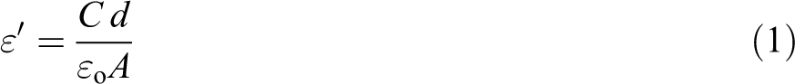


where d is the thickness of the composite film (m), A is the area of the copper plate (m2), ω is angular frequency, that is, 2πf and f is the applied frequency (Hz) and ε 0 is the permittivity of a free space (8.85 × 10⁻¹² F m−1).
Results and discussion
Materials characterizations
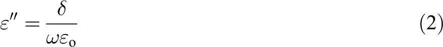
FTIR spectra of fGNPs revealed successful functionalization as shown in Figure 2(a). Vibration bands at 2150, 2028 and 1973 cm−1 represent major peaks of GNPs. Additional peaks were observed after functionalization due to attached functional groups. For instance, C=O and C=C vibration bands represented at 1732 and 1604 cm−1 were respectively observed with fGNPs. Peak at 1535 cm−1 can be attributed to the stretch of amine groups such as N–H. Also, there were deformation vibrations of C–O and C–H represented at 1118 and 1406 cm−1, respectively. These vibrations are believed to be the results of increase in oxygen content on fGNPs and little introduction of defects (sp3 domain) on the basal plane of fGNPs. 32 Raman analysis revealed major peaks of graphene and level of sp2 network destruction after functionalization as shown in Figure 2(b). The peaks at 1365 and 1585 cm−1 for GNPs represent D and G bands, respectively. The G band arose due to first-order scattering and vibration of E2g phonon by carbon atoms. While the D band was due to reduction in sp2 domain and introduction of sp3 hybridized carbon popularly known as disordered structure. 22,33 For pristine graphene, the D band intensity (I D) is believed to be close to zero. For the graphene used in this study, there is relatively an increase in D band because it was slightly oxidized on purchase. However, there was no deep destruction of sp2 network domain of the GNPs, because intensity ratio of D to G bands (I D/I G) was relatively low (about 0.25) compared to highly oxidized graphene previously reported by Kuila et al. 31 and Maity et al. 22 This contributed to only little further increase in sp3 domain within sp2 network structure as I D/I G only increased to 0.37 after functionalization. Also, the weaker D band intensity of GNPs compared to fGNPs and shift in D band to 1379 cm−1 with fGNPs showed successful functionalization.
(a) FTIR spectra, (b) Raman spectra of fGNPs and GNPs and (c) FTIR spectra of the co-fabricated composite samples.
Phases present in the composites and interaction between fGNPs and PVDF matrix were revealed by FTIR as shown in Figure 2(c). The peaks at 530, 618, 766, 798, 980 and 1386 cm−1 are creditable to α-phase of the composites, while β-phase in the composites is represented by vibration bands at 840 and 1278 cm−1. 22 Notably, there was continuous increase in β-phase at 840 cm−1 and 1278 cm−1 with addition and increase in fGNPs content. Also, the vibration stretches were observed to have shifted to higher energy with incorporation of fGNPs in the polymer matrix. This can be attributed to good interaction between fGNPs and PVDF matrix, which resulted from attached functional groups on fGNPs as revealed by FTIR spectra in Figure 2(a). The β-phase which is responsible for piezoelectric properties, contributed to enhancing dielectric performance recorded in this study.
Morphology of the composite samples
Morphology of the composites was investigated as shown in Figure 3. There was no significant agglomeration of graphene in PVDF matrix for co-fabricated composites (fG/PVDF-S/M) as shown in Figure 3(a) and (b). This can be attributed to the functionalization of GNPs, which improved hydrogen bonding between functional groups on fGNPs and fluorine atoms in the PVDF matrix. Also, during melt mixing of the composites, the rotating screw enhanced proper mixing and dispersion of graphene in the matrix. This encouraged more polymer to graphene contact than graphene to graphene contact and resulted in strong interfacial interaction with the polymer matrix. On the other hand, some level of debonding and agglomeration can be seen with solution blended-only composites (fG/PVDF-S) as shown in Figure 3(d) and (e) compared to fG/PVDF-S/M composites, which is attributable to improper mixing and re-clustering of graphene in the matrix. This indicates that further dispersion of graphene after solution mixing can be achieved by melt mixing. Also, it was noted from EDS analysis that oxygen content of the composites was significantly reduced after melt mixing. After solution blending, oxygen percentage recorded was about 21.87 wt% as shown in Figure 3(f). While the oxygen content dropped to 2.78 wt% after proceeding to 15-min melt compounding as shown in Figure 3(c). This is about 87.3% reduction in the oxygen content of the composite. This indicates that the modified graphene was in situ thermally reduced, which led to the recovery of graphene structure with enhanced composites dielectric performance and energy storage capability.
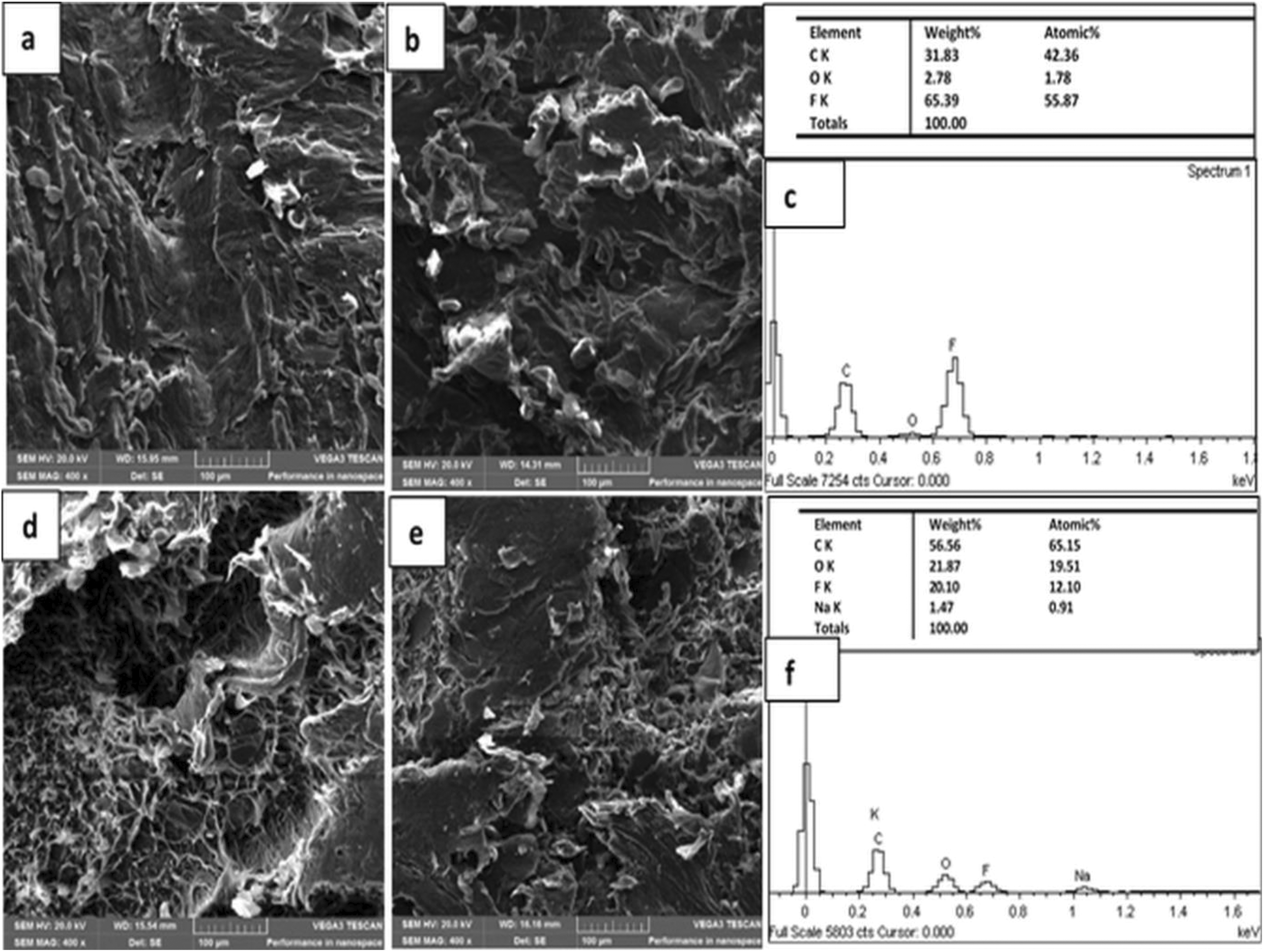
SEM images of (a) 3.34 wt%fG/PVDF-S/M and (b) 6.67 wt%fG/PVDF-S/M; (c) EDS of 6.67 wt%fG/PVDF-S/M, (d) 3.34 wt%fG/PVDF-S, (e) 6.67 wt%fG/PVDF-S; and (f) EDS of 6.67 wt%fG/PVDF-S composites.
Dielectric and electrical properties
All composite samples showed significant increase in dielectric constant (ε′) compared to neat PVDF as shown in Figure 4(a). Dielectric constant of neat PVDF was recorded as approximately 9 at 100 Hz. It was later increased to about 2616 with 1.67 wt%fG/PVDF-S/M composite, which is about 289 times higher than that of neat PVDF. The increase in ε′ can be attributed to large surface area and high aspect ratio of graphene. Also, 2D structure of graphene sheets gives them plate-like surfaces in the polymer matrix, with high tendency to form mini-capacitors when adjacent graphene sheets are separated by thin layers of polymer. 3 Effective mini-capacitance of mini-capacitors in polymer matrix gives capacitance of the composite, which is proportional to ε′ of the composite. Therefore, increase in mini-capacitors in the polymer matrix can result in increase in ε′ of the composite. This explains the reason for higher ε′ (about 38418 at 100 Hz) obtained with 6.67 wt%fG/PVDF-S/M composite. According to Maxwell–Wagner–Silas’s theory, heterogeneous accumulation of charge carriers on the interfaces of graphene and polymer layers contributed to the enhanced ε′ recorded with addition of graphene. 34 It was noted that all composites showed sharp reduction in ε′ with frequency, while neat PVDF exhibited slight decrease with frequency. This is due to the formation of high conductive grain boundaries in the polymer matrix with the addition of graphene at high frequency in favour of low ε′. 35 Such high conductive grain boundaries may not be present in neat PVDF. Also, difference in equilibrium relaxation between graphene and PVDF molecular chains contributed to the variation in the reduction of ε′ with frequency.
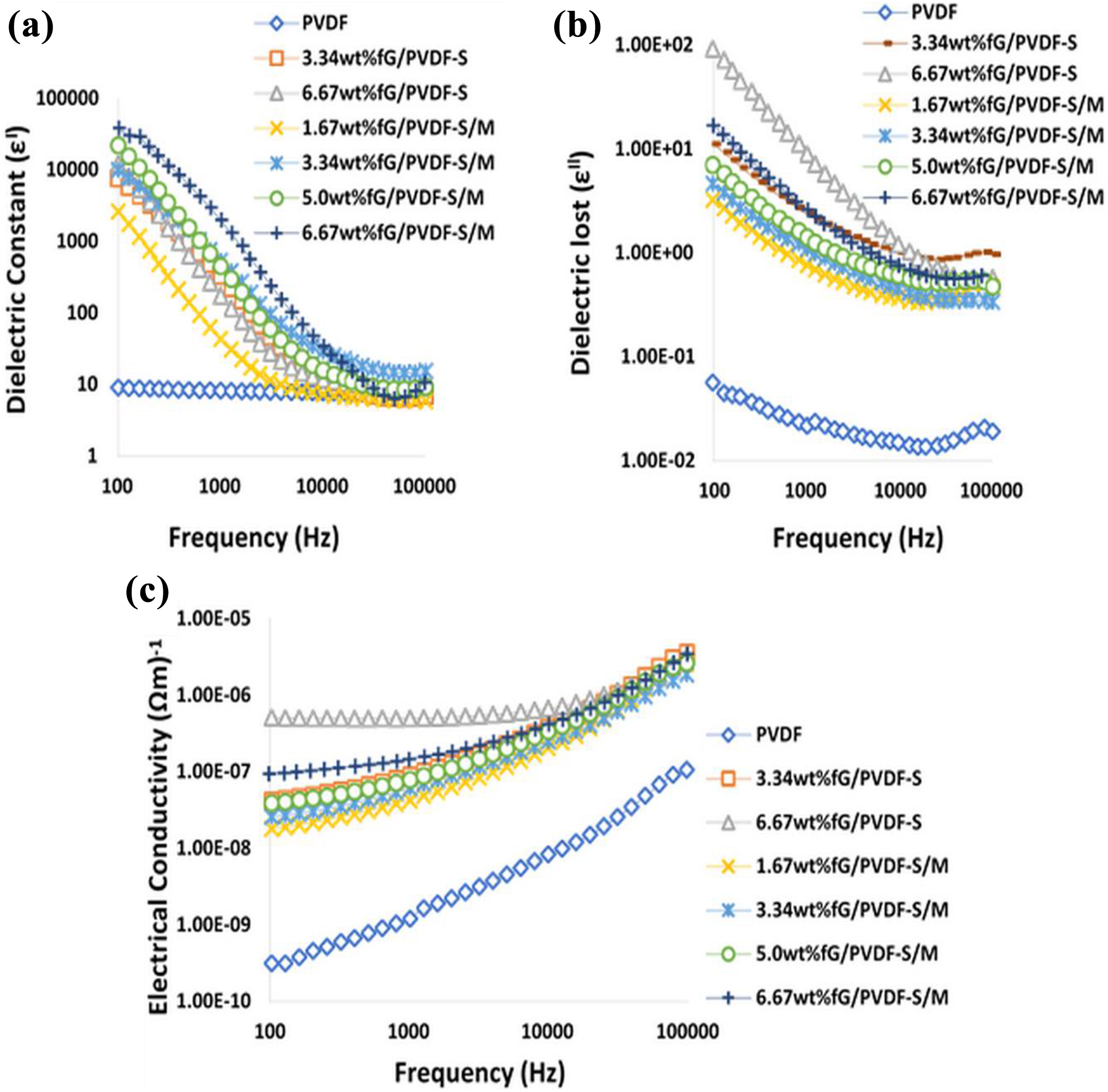
(a) Dielectric constant, (b) dielectric loss and (c) electrical conductivity of the composite samples.
fG/PVDF-S/M composites showed higher ε′ compared to fG/PVDF-S composites at all similar concentrations. For instance, ε′ of about 9930 and 38,418 were recorded with 3.34 wt%fG/PVDF-S/M and 6.67 wt%fG/PVDF-S/M composites at 100 Hz, respectively. While 7588 and 12,046 were respectively recorded with 3.34 wt%fG/PVDF-S and 6.67 wt%fG/PVDF-S composites. These are respectively about 30.8% and 218.9% increase in ε′ with the former composites compared to the later composites. The higher ε′ recorded for fG/PVDF-S/M composites are traceable to their homogeneous dispersion and strong bonding between the composites’ constituents as shown by SEM images in Figure 3(a) and (b) due to proper mixing of graphene during melt compounding. Also, reduction of oxygen content in fG/PVDF-S/M composites (Figure 3(c)) compared to fG/PVDF-S composites (Figure 3(f)) contributed to the higher ε′. This is because graphene with high oxygen content behaves like insulator, 36 with poor electrical and thermal conductivity, thereby forming insulative plate-like sandwich structures with thin layers of polymer matrix, instead of conductive plate-like sandwich structures.
Figure 4(b) shows dielectric loss (ε″) of the composite samples. At 100 Hz, ε″ of about 0.056 was recorded for neat PVDF and increased to 3.23 for 1.67wt%fG/PVDF-S/M composite. The increase in ε″ can be attributed to increase in mobility of free electrons and π-orbital electrons with the addition of graphene. When graphene content increased to 3.34 wt%, 5.0 wt% and 6.67 wt%, ε″ increased to 4.62, 7.01 and 16.8, respectively, for fG/PVDF-S/M composites at 100 Hz. The continuous increase in ε″ with increasing graphene content may be ascribed to formation of conductive networks and current leakage resulting from direct contact of graphene in the matrix. 15 On the other hand, reduction in polymer insulating barrier between adjacent graphene sheets with increasing graphene content encouraged easy jumping of charge carriers from one graphene sheet to another. This led to high current leakage which is one of the reasons for increased ε″ observed with higher graphene concentration. Comparing ε″ of fG/PVDF-S/M and fG/PVDF-S composites, it can be seen from Figure. 4(b) that ε″ of fG/PVDF-S composites are higher compared to fG/PVDF-S/M composites at all similar graphene concentrations. For instance, ε″ of about 92.4 was recorded for 6.67 wt%fG/PVDF-S composite, while 16.8 was recorded for 6.67 wt%fG/PVDF-S/M composite at 100 Hz. This is about 81.8% reduction in ε″ compared to 6.67 wt%fG/PVDF-S composite. Therefore, one can say that homogeneous dispersion and strong interfacial interaction are essential for low ε″, which was achieved in this study by co-fabrication approach.
Electrical conductivity of the composite samples is shown in Figure 4(c). Low electrical conductivity of about 3.14E−10 (Ωm)−1 at 100 Hz was measured for neat PVDF. The conductivity increased gradually with the addition of graphene. At 100 Hz, electrical conductivities of about 1.79E−8 (Ωm)−1, 2.57E−8 (Ωm)−1 and 1.0E−7 (Ωm)−1 were recorded for 1.67 wt%fG/PVDF-S/M, 3.34 wt%fG/PVDF-S/M and 6.67 wt%fG/PVDF-S/M composites, respectively. These observations were due to the formation of conductive networks, increase in the number of free electrons and high mobility of charge carriers in PVDF matrix with the increase in graphene content. However, the conductivities were lower when compared to that of fG/PVDF-S composites. This can be attributed to high level of agglomeration observed for fG/PVDF-S composites, which encouraged higher level of direct contact of graphene sheets in PVDF matrix with higher electrical conductivity and current leakage compared to fG/PVDF-S/M composites.
Breakdown strength and energy storage density
Figure 5(a) shows breakdown strengths (E) of the composite samples. E of the samples were decreasing with the addition and increasing graphene content. This is accountable to reduction in polymer layers and shorter distance between adjacent graphene sheets as graphene content increases, thereby resulting in the increase in tunnelling of charge carriers through the polymer barrier and easy transfer of electrons from one graphene sheet to another when electric field was applied. Breakdown strength of about 293 kV cm−1 was measured for neat PVDF, which decreased to 22 kV cm−1 and 18 kV cm−1 for 3.34 wt%fG/PVDF-S and 6.67 wt%fG/PVDF-S composites, respectively. However, fG/PVDF-S/M composites showed higher E compared to fG/PVDF-S composites at all similar graphene contents. For instance, E of about 32 kV cm−1 and 22 kV cm−1 were respectively recorded for 3.34 wt%fG/PVDF-S/M and 6.67 wt%fG/PVDF-S/M composites. The increase in E of fG/PVDF-S/M composites compared to fG/PVDF-S composites is traceable to their variations in dielectric loss and electrical conductivity as shown in Figure 4(b) and (c). Because the dielectric loss of fG/PVDF-S composites were higher than fG/PVDF-S/M composites, fG/PVDF-S composites were expected to have lower E. These variations in E of the composites fabricated by single and double routes are also traceable to dispersion and bonding of graphene with the matrix as shown in Figure 3, where fG/PVDF-S/M composites had better dispersion of graphene and resulted in higher E compared to fG/PVDF-S composites. At lower graphene content of 1.67 wt%, appreciable E of about 40 kV cm−1 was recorded but still far lower than neat PVDF due to the introduction of free electrons and other charge carriers in the matrix.
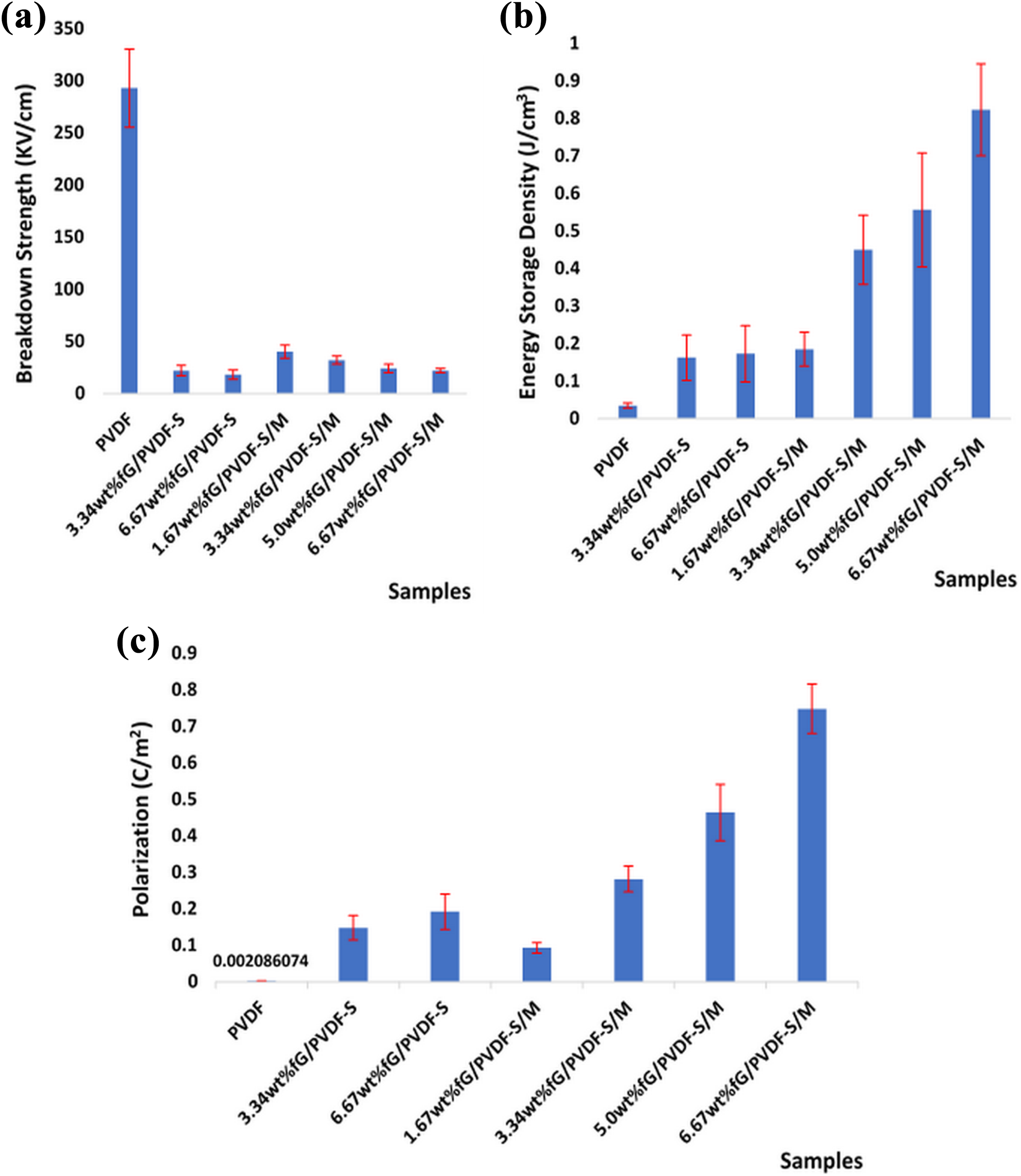
(a) Breakdown strength, (b) energy storage density and (c) polarization of the composite samples.
Notwithstanding the relatively low E of the composite materials, their high dielectric constants had significant influence on their energy storage density as shown in Figure 5(b) and Table 1. Energy storage density (Ub ) was lower with neat PVDF due to its inherent low ε′ compared to the composite materials. Approximately, Ub of about 0.0346 J cm−3 was calculated for neat PVDF. While about 0.1852 J cm−3 was recorded with 1.67 wt%fG/PVDF-S/M composite, which is about 435.3% increment. This enhancement was due to the significant increase in ε′ of the composite. On the other hand, fG/PVDF-S/M composites showed higher Ub compared to fG/PVDF-S composites. For instance, 3.34 wt%fG/PVDF-S and 6.67 wt%fG/PVDF-S composites gave Ub of about 0.1625 J cm−3 and 0.1727 J cm−3, while 0.4500 J cm−3 and 0.8228 J cm−3 were calculated for 3.34 wt%fG/PVDF-S/M and 6.67 wt%fG/PVDF-S/M composites, respectively. These are about 176.9% and 376.4% increase in Ub compared to their counterparts. The observations are accountable to low current leakage, high dielectric constant and low dielectric loss of fG/PVDF-S/M composites. The improved Ub of the composites when compared to neat PVDF was due to enhanced polarization with the addition of graphene as shown in Figure 5(c) and Table 1. Polarization is the distortion of electron clouds and separation of positive and negative charges with the application of electric field. It played important role in enhancing ε′ of the composites. From Table 1, increase in ε′ of the composites depends on increase in polarization. Notably, polarizations of fG/PVDF-S/M composites were higher than that of fG/PVDF-S composites. This indicates that strong adhesion between layers of polymer and graphene is essential for the accumulation of charges at their interfaces. This was achieved by functionalization of graphene and the two-way fabrication approach used in the preparation of composites.
Dielectric constant at 100Hz, breakdown strength, energy storage density and polarization of the samples.
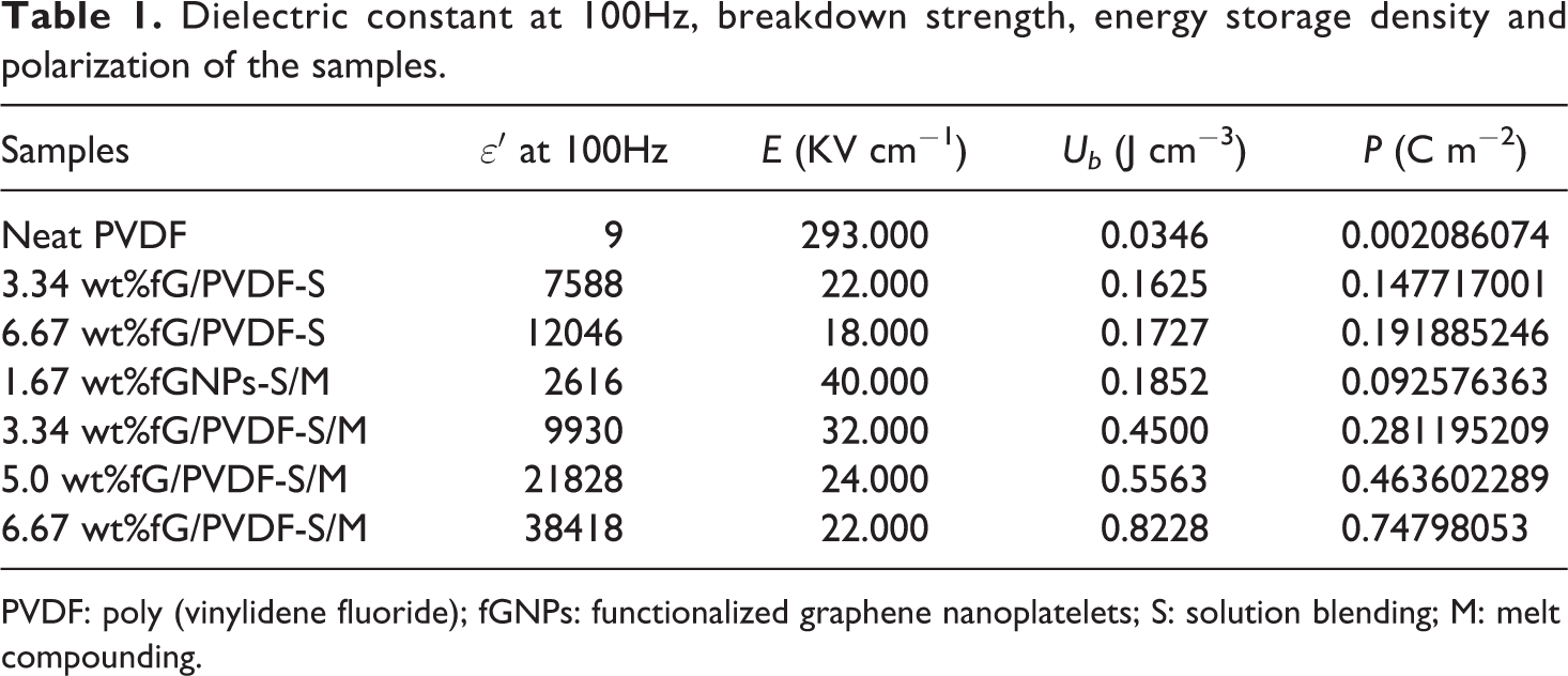
PVDF: poly (vinylidene fluoride); fGNPs: functionalized graphene nanoplatelets; S: solution blending; M: melt compounding.
Conclusion
In this study, GNPs were successfully functionalized as revealed by FTIR and Raman analysis. Microstructural study of the samples showed better interfacial interaction and dispersion of graphene with fG/PVDF-S/M composites compared to fG/PVDF-S composites. From the results obtained, dielectric constant of all composites was significantly enhanced. But dielectric performance of fG/PVDF-S/M composites were better due to their higher polarization compared to fG/PVDF-S composites. This was attributed to the two-way processing approach used in the preparation of fG/PVDF-S/M composites, which encouraged further dispersion of graphene in the PVDF matrix and intercalation of graphene with PVDF molecular chains. Also, in situ thermal reduction of modified graphene during melt compounding contributed to enhanced dielectric performance and energy storage capability of fG/PVDF-S/M composites. For instance, energy storage density increments of about 176.9% and 376.4% were recorded for 3.34 wt%fG/PVDF-S/M and 6.67 wt%fG/PVDF-S/M composites, when compared to fG/PVDF-S composites at similar graphene concentrations, respectively. Therefore, the fabrication approach used for the composites preparation in this study is a feasible approach to achieve PGNs with advance energy storage density for capacitors and other engineering applications.