
Abstract
In this research, transparent titania (TiO2) thin films were deposited on a glass microscope slide and on a flexible polyethylene terephthalate (PET) substrate under a high vacuum condition by means of the thermionic vacuum arc (TVA) method in a very short period of time (60 s). Optical properties and surface properties of the coated TiO2 surfaces are related to the structural changes of the coated layers due to ion energies and substrate effect. But obtained results are closely linked to literature values. Our analysis showed that the TVA method is an alternative method for low-temperature coatings and the produced films present important advantages for optical and industrial applications.
Keywords
Introduction
Titania (TiO2) is a medical and technologically important material. These materials are used in dental materials 1 and wide bandgap semiconductor. 2 –17 TiO2 material is used for numerous applications such as photocatalytic reactivity, 3,5 resistive switching, 2 –4 optoelectronic applications, 9 photoelectrochemical applications, 10 waveguiding, semiconductor, storage capacitor, 12 and, so on. TiO2 is transparent to visible light with many other interesting properties such as a high refractive index, high dielectric constant, high chemical stability, excellent mechanical durability, and high photocatalytic reactivity. 2 –17
TiO2 thin films can be produced by numerous techniques such as ion beam deposition system, 1 atomic layer deposition, 2 liquid phase deposition, 3 plasma-enhanced atomic layer deposition, 4 ionized cluster beam, 6 and sputtering methods. 7,8,11,12 However, the structure and the other properties of TiO2 thin films depend strongly on the deposition technique and parameters. 1 –17 TiO2 samples have been grown in three crystal structures. These are called as rutile, anatase, and brookite. 6,8,9
In this research, the properties of the semiconductor application of the TiO2 for composite materials are presented. Thermionic vacuum arc (TVA) method was employed for TiO2 thin films for the first time. TVA is a plasma-assisted deposition technique. Compared to other plasma-assisted techniques, TVA has a number of significant advantages such as enabling the production of pure, compact, smooth, nanostructured, homogenous, and cohesive thin films. Besides, the method is remarkably rapid to employ with low working budgets and high deposition rate. 18 –21
Experimental
TVA was performed for the deposition of the TiO2 thin films on a glass and transparent flexible polyethylene terephthalate (PET) substrate for the first time. A schema of the experimental setup can be seen in Figure 1. 21
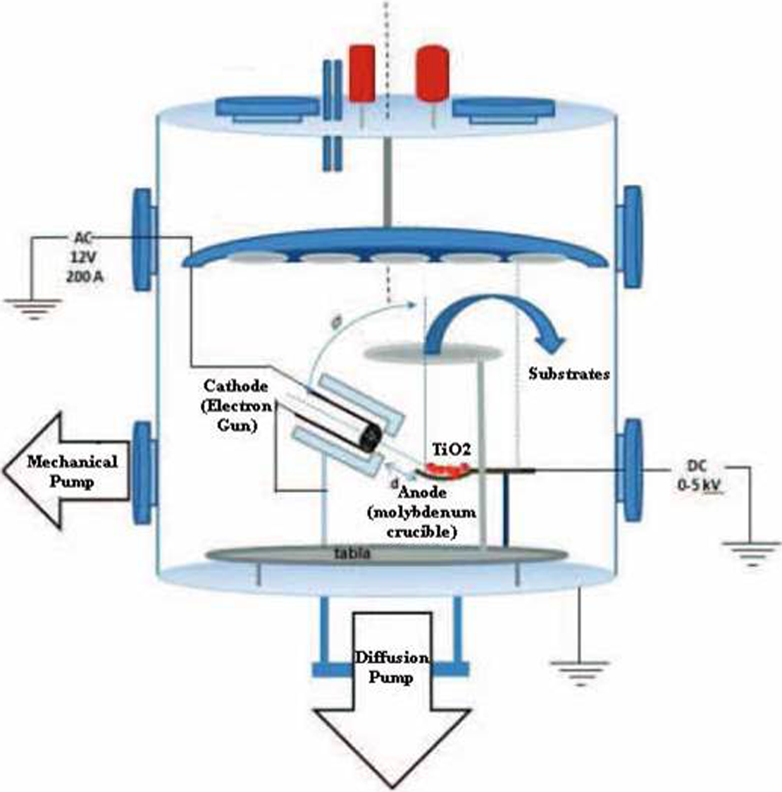
A schematic of the experimental setup.
The end pressure was adjusted to approximately 10−6 torr. Deposition was realized at this vacuum level without any buffer gas. As an anode material, TiO2 pellets were used. The anode material is in rutile and anatase crystal formation. According to X-ray diffraction data of the deposited layer by TVA, TiO2 layers are composed of rutile and anatase. The distance between the anode and the cathode was approximately 3–4 mm. The substrates were placed at a distance around 80 mm. The filament current applied to the cathode was 19 A. The voltage applied to the space between anode and cathode was 450 V. The discharge current created between anode and cathode was approximately 1A. The deposition process was carried out for 60 s. These are the critical parameters. Other parameters were kept constant.
The properties of the produced TiO2 films were analyzed using various tools: Spectroscopic ellipsometer (SE) for thickness and refractive index determinations, UNICO 4802 ultraviolet–visible (UV-Vis) spectrophotometer for optical measurements of transmittance and absorbance, JEOL-JSM 5600LV field emission scanning electron microscope (FESEM; Japan) and Ambios Q-Scope atomic force microscope (Ambios Technology, Santa Cruz, California, USA) for surface investigation and Attention Tensiometer Theta Lite for surface contact angle measurements. Also, the optical bandgaps were estimated from the Tauc plot.
Results and discussion
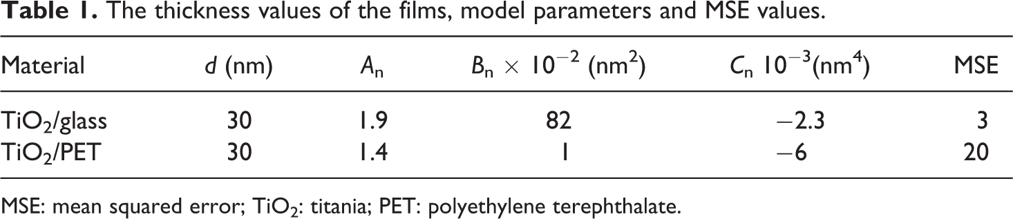
SE is an important device for the nondestructive analysis method to determine the optical constants of the coated layers with different fitting models. This device is widely used to determine the thickness (d) and the optical constants of a thin film including the refractive index (n) and the extinction coefficient (k). SE spectra of the produced samples in this article were recorded in the wavelength range between 300 nm and 1000 nm. Brewster angle was determined experimentally as 65°. Brewster angle value is fairly isomorphic with the presented values in the related literature. 12,15 Many curve fitting models are used for optimization of obtained SE results. 12,15 In this article, Cauchy dispersion model and mean squared error (MSE) values were determined for the deposited TiO2 samples on glass and PET substrates.
In the Cauchy dispersion model, the refractive index n(λ) as a function of the wavelength is given by,

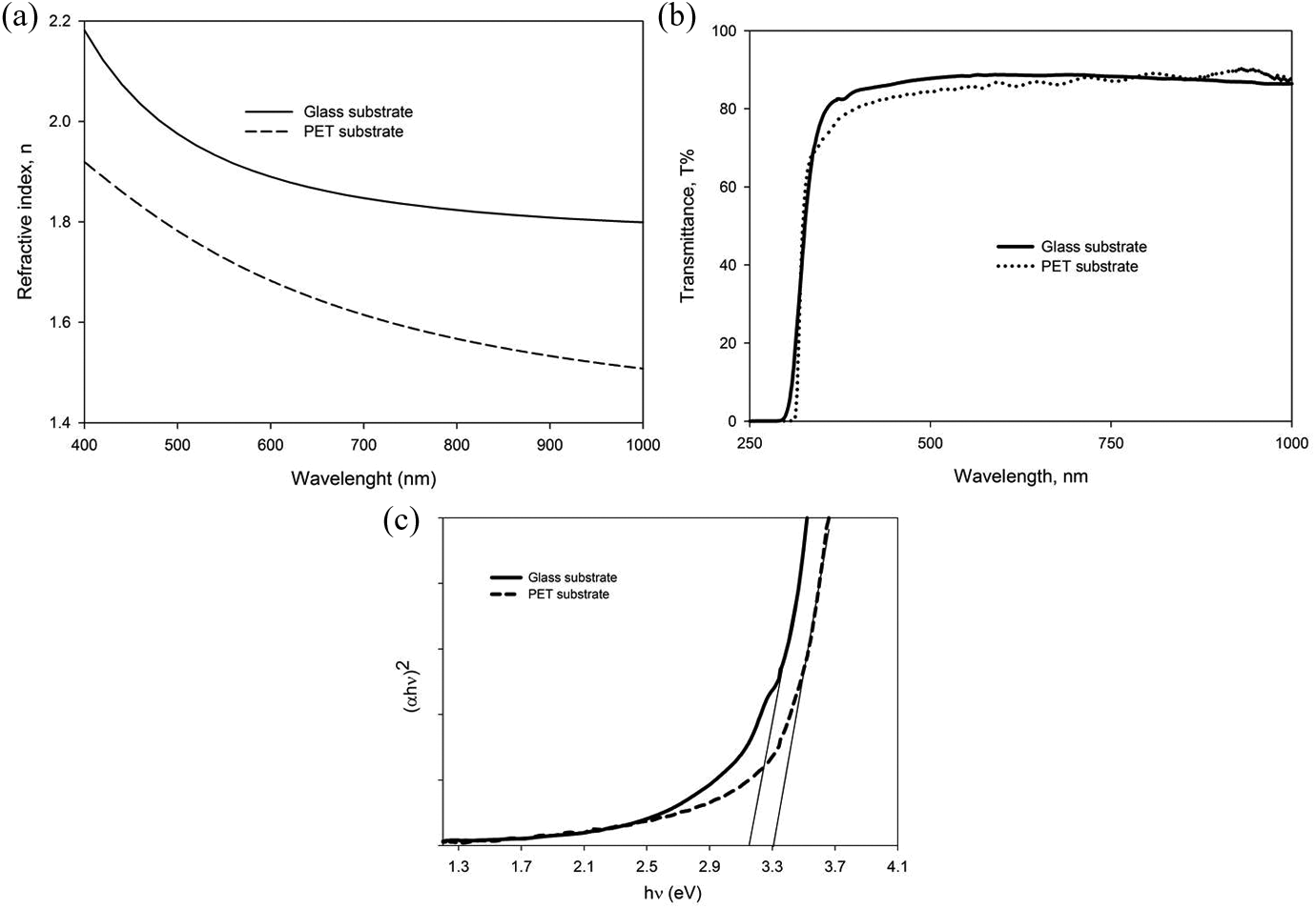
(a) Refractive index, (b) transmittance, and (c) Eg band gap energies of the deposited TiO2 thin films on glass and PET substrates.
The thickness values of the films, model parameters and MSE values.
MSE: mean squared error; TiO2: titania; PET: polyethylene terephthalate.
As shown in Figure 2(a), the refractive indices of the produced TiO2 films decreased with the increasing wavelength. The refractive index values of the film deposited on the PET substrate were found to be lower than those of the film deposited on the glass substrate. These values are also lower than the reported values in the relevant literature, 9,11,12,15 because the production method strongly affected the densities and packing structures.
The optical transmittances of the produced films were determined in the wavelength range between 200 nm and 1100 nm (Figure 2(b)). Interference fringes are seen in Figure 2(b), and amplitude of the fringes are very small.
5,9
The optical bandgaps of the produced TiO2 films were estimated from the Tauc plot based on the relation
The AFM images of the produced TiO2 films are shown in Figure 3(a) and (b). The root mean square of the roughness of the deposited TiO2 films is approximately 2 nm for the film on the glass and PET substrate. The FESEM images are shown in Figure 3(c) and (d). According to Figure 3(d), surface cracks caused by the thermal expansion of the PET surface were detected. The wavelength-dispersive spectroscopy (WDS) results are given in Table 2. Surface properties such as roughness and compactness and, so on. are also related with the ion energy flux.
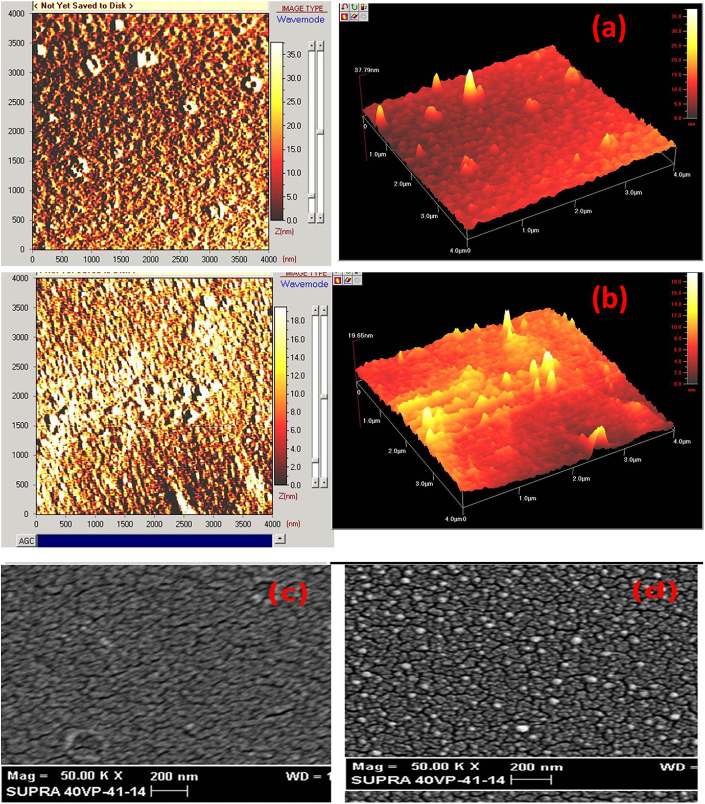
2D and 3D images of the produced TiO2 thin film (a) on glass substrate (b) on PET substrate. FESEM images of the produced TiO2 thin film (c) glass substrate and (d) PET substrates. TiO2: titania; PET: polyethylene terephthalate substrate; FESEM: field emission scanning electron microscopic.
The WDS results of the produced TiO2 films.
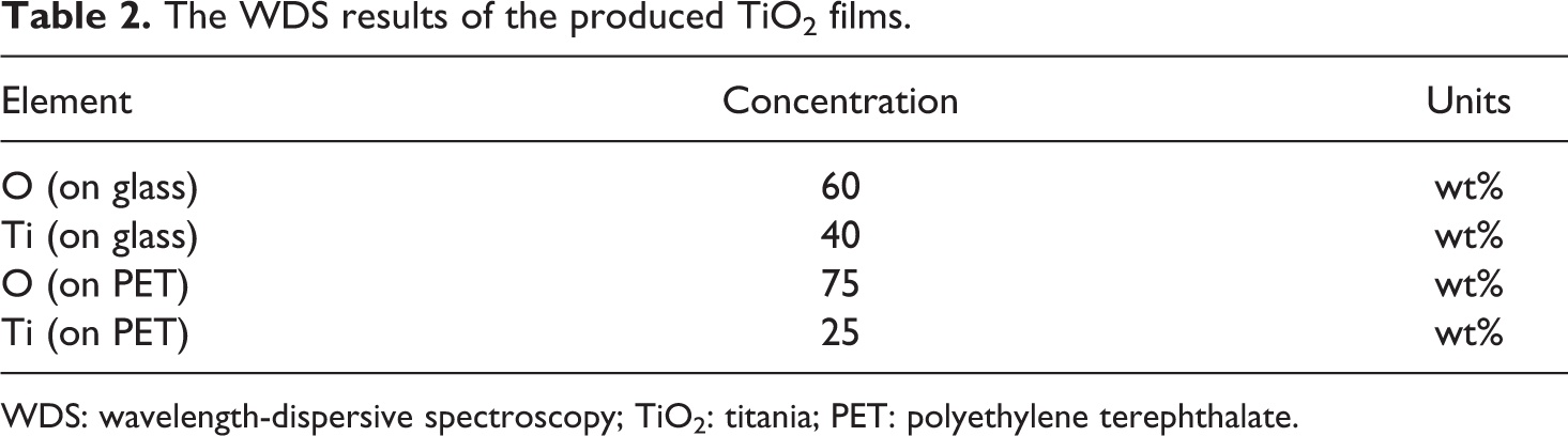
WDS: wavelength-dispersive spectroscopy; TiO2: titania; PET: polyethylene terephthalate.
For the wettability property determination of the samples, an optical tensiometer was used. The measured contact angle (CA) value of the film deposited on the glass substrate is about 70° and it is about 85° for the film deposited on the PET substrate. The contact angles for an uncoated glass substrate and PET substrate are 30° and 70°, respectively. In this regard, a surface coated with TiO2 exhibits more hydrophobic surface characteristics.
Conclusion
TVA is a different type of plasma-assisted deposition technique performed for the manufacturing of the TiO2 thin films on different substrates in only 60 s. The produced TiO2 films were found to be wide bandgap semiconductors at approximately 3.2–3.3 eV. Produced samples have demonstrated high optical transmittance. Optical and surface properties of the produced TiO2 films rely on the production method employed and substrate materials used. PET subtrates can be coated by TVA easily. The TiO2 thin films can be deposited at room temperature using TVA.
Footnotes
Declaration of Conflicting Interests
The author(s) declared no potential conflicts of interest with respect to the research, authorship, and/or publication of this article.
Funding
The author(s) received no financial support for the research, authorship, and/or publication of this article.