
Abstract
The influence of thermal annealing on the performance of a poly(3-hexylthiophene-2,5-diyl) (P3HT) and [6,6]-phenyl-C61-butyric acid methyl ester (PCBM) organic solar cells with an aluminum cathode was systematically investigated for varying active-layer thicknesses. Devices were fabricated using single (10 mg·ml−1) and double (20 mg·ml−1) P3HT concentrations, and the effect of spin-coating speed on film morphology and device performance was evaluated. Pre- and post-annealing treatments were applied at 100, 120, 140, and 160 °C for 30 minutes, with a two-step post-annealing process at 160 °C for 30 minutes followed by 180 °C for 10 minutes. Optical absorption spectroscopy, atomic force microscopy, and current–voltage measurements were employed to assess the effects on light harvesting and photovoltaic parameters. The highest efficiency of 2.1% was achieved for an 80-nm-thick film prepared at 1000 rpm with double-concentration P3HT after the two-step post-annealing. This treatment increased the optical absorption of the active layer by 12% and enhanced device performance, resulting in a 5.8% power conversion efficiency improvement. The results highlight the critical role of annealing temperature, timing, film thickness, and spin-coating speed in optimizing P3HT:PCBM OSC performance.
Introduction
Organic solar cells (OSCs) have attracted significant attention in the field of renewable energy due to their unique advantages, including mechanical flexibility, lightweight, portability, and low-cost fabrication (Kim et al., 2006; Ma et al., 2005; Mahmoud et al., 2012, 2013, 2014). The bulk heterojunction (BHJ) architecture, formed by blending electron-donor and electron-acceptor materials, has emerged as the most successful OSC design. This structure facilitates efficient exciton dissociation via a self-assembled, interpenetrating network of donor (polymer) and acceptor (fullerene) materials (Chandrasekaran et al., 2021; Ho et al., 2011; Jiang et al., 2021).
Among the variety of donor polymers, poly(3-hexylthiophene-2,5-diyl) (P3HT) is widely studied owing to its favorable optoelectronic properties, including high hole mobility (10−4 to 10−2 cm2 V−1 s−1) [9], chemical stability, low bandgap, high crystallinity, and strong light absorption up to 650 nm (Helmut et al., 2007; Ho et al., 2011; Kim et al., 2006; Li et al., 2005; Ma et al., 2005). On the acceptor side, [6,6]-phenyl-C61-butyric acid methyl ester (PCBM) is a commonly used fullerene derivative. Its solubility in typical polymer solvents allows for easy processing, and its high electron mobility enables rapid exciton dissociation and charge transport (Hauff et al., 2005; Sariciftci et al., 1992). Figure 1 shows the chemical structures of P3HT and PCBM.
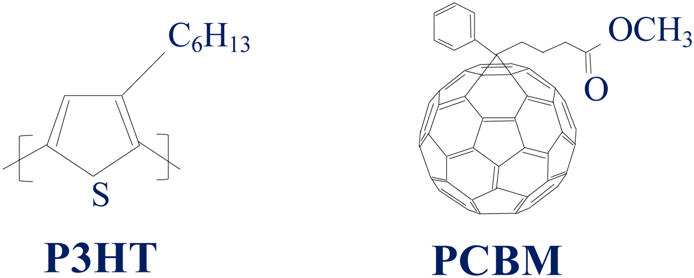
The chemical formulas for P3HT polymer and PCBM fullerene.
The photocurrent generation process in OSCs is more complex than in conventional inorganic solar cells. As illustrated in Figure 2, when illuminated with photons of sufficient energy (∼1.8 eV), the polymer absorbs light and generates excitons. These excitons diffuse over a short range (∼10–20 nm) and, upon reaching donor–acceptor interfaces, dissociate into polaron pairs. The applied electric field then drives the resulting free electrons and holes to the respective electrodes, generating a photocurrent (Cook et al., 2009; Deibel, 2025).
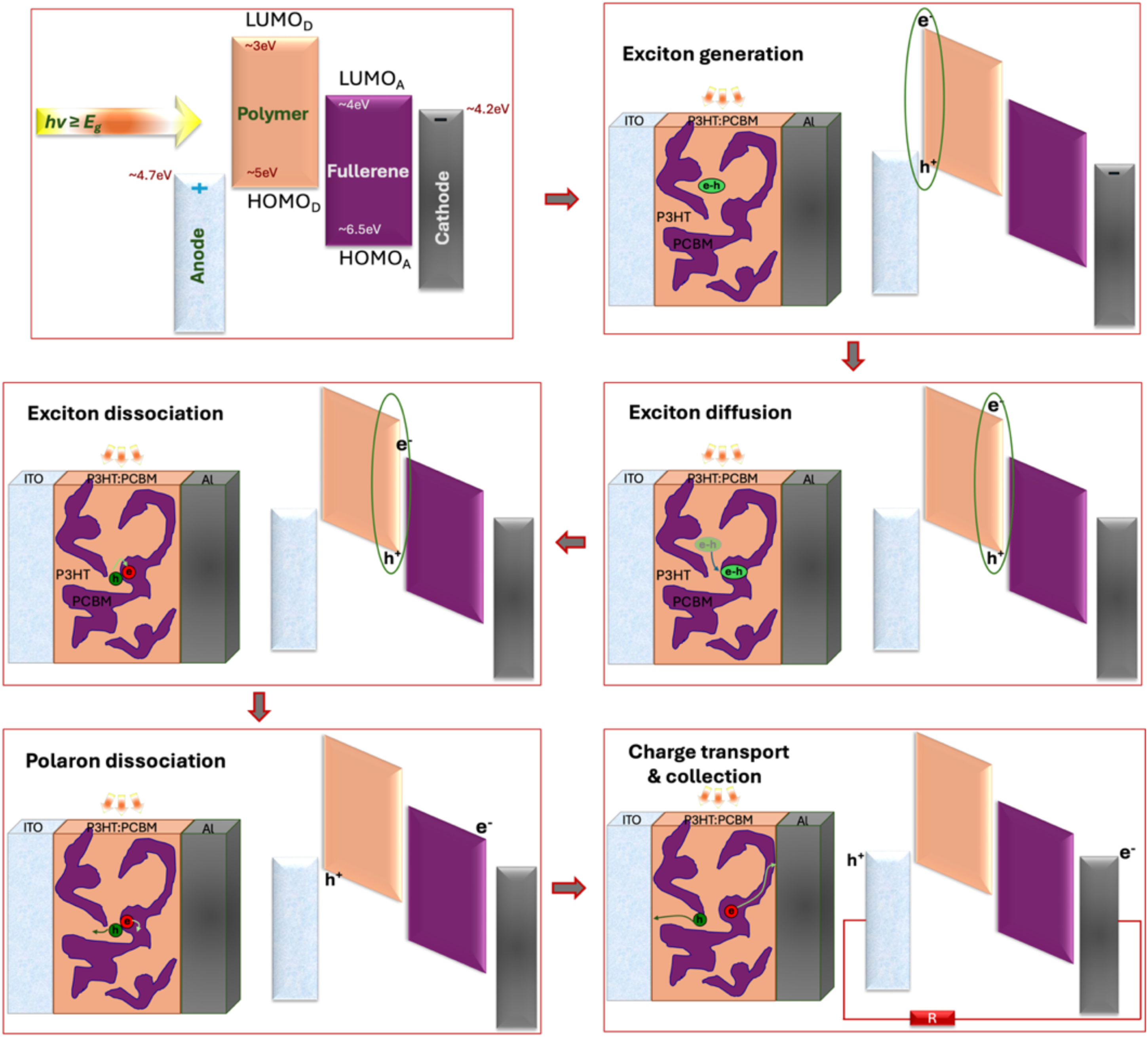
The charge transport mechanism in Polymer: Fullerene solar cells.
Despite significant progress, BHJ OSCs based on P3HT:PCBM blends have achieved only moderate power conversion efficiencies (PCE) of approximately 4% to 6% (Aaqib et al., 2024; Alam et al., 2022; Kim et al., 2010; Shin et al., 2011). This efficiency remains insufficient for OSCs to compete with inorganic or other high-performance photovoltaic technologies.
Equivalent circuit and photovoltaic parameters
The solar cell equivalent circuit (Figure 3) describes the current–voltage (J–V) behavior (Ma et al., 2005; Moliton and Nunzi, 2006):


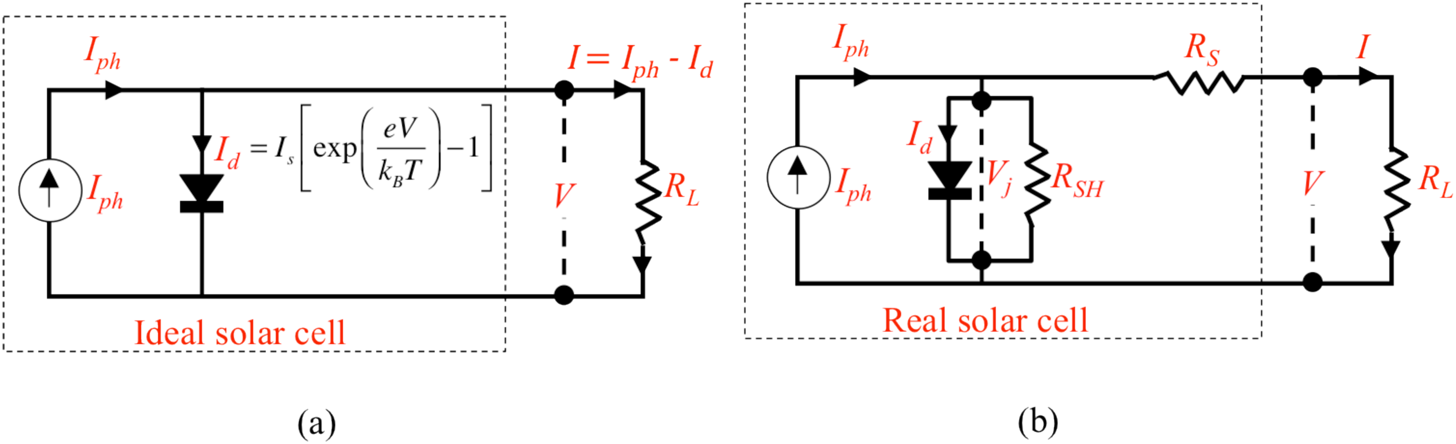
Schematic diagrams for the equivalent circuit of (a) an ideal solar cell connected to the load RL; (b) a real solar cell in which both RSH and RS are considered, Vj = V + IRS is the voltage across the junction [re-drawn from Moliton and Nunzi, 2006].
From the above equations, it is evident that minimizing the RS and maximizing the RSH are essential for achieving higher PCE. While increasing the active-layer thickness enhances light absorption, the concomitant rise in RS can limit further improvements in device efficiency. Therefore, enhancing JSC through the reduction of series resistance represents a key strategy for PCE optimization (Lee, et al., 2009; Shen et al., 2009; Zidan et al., 2021).
Thermal annealing is a critical step in the fabrication of OSCs, as it improves both the morphological and optical properties of the active layer, leading to enhanced PCE (Kim et al., 2002; Shaban et al., 2021). Annealing facilitates reduced series resistance and promotes more ordered nanoscale morphology in the polymer:fullerene film (Li et al., 2005; Lu et al., 2011; McNeill et al., 2008; Orimo et al., 2010; Sánchez et al., 2020). Moreover, the timing of thermal treatment—whether performed before (pre-annealing) or after (post-annealing) cathode deposition—has a significant impact on device performance (Balogun et al., 2018; Erb et al., 2005; McNeill et al., 2008; Shaban et al., 2021). Despite previous studies, there remains a need to establish a reliable and reproducible annealing protocol.
Although P3HT:PCBM BHJ OSCs have been extensively studied, several critical factors still limit their performance. The interplay between active-layer thickness, morphology, and processing conditions—particularly thermal annealing timing and temperature—remains inadequately understood. While thermal annealing is known to improve film crystallinity, reduce series resistance, and enhance exciton dissociation, a systematic investigation linking annealing parameters with active-layer thickness and spin-coating conditions is lacking. Establishing a reliable annealing protocol tailored to different film thicknesses is therefore essential for optimizing P3HT:PCBM OSC performance and achieving higher PCE.
In this context, the interplay between thermal annealing and active-layer thickness represents a rich area for optimization. The present study provides systematic data to develop a robust annealing procedure for BHJ P3HT:PCBM solar cells with aluminum cathodes, focusing on the effects of thermal treatment across different active-layer thicknesses to achieve high-efficiency devices.
Experimental details
Active layer materials and solutions preparation
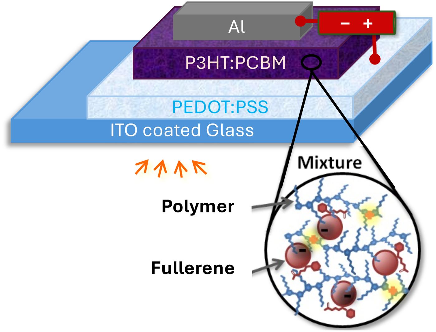
Poly(3-hexylthiophene) (P3HT, regioregularity 98%, average molecular weight <50,000 g·mol−1) was obtained from Rieke Metals, while [6,6]-phenyl C₆₁ butyric acid methyl ester (PCBM, >99.5%) was purchased from Sigma-Aldrich. The buffer layer poly(3,4-ethylenedioxythiophene):poly(styrenesulfonate) (PEDOT:PSS) solution (Baytron P VPAI 4083) was purchased from HC Stark. The active layer solutions were prepared by dissolving P3HT and PCBM in anhydrous 1,2-dichlorobenzene (99%) at a fixed weight ratio of 1:0.8. Two polymer concentrations were formulated: 10 mg ml−1 (single concentration) and 20 mg ml−1 (double concentration). All solutions were prepared inside a nitrogen-filled glove box and stirred vigorously overnight at room temperature to ensure complete dissolution and optimal homogeneity.
Device fabrication
Figure 4 illustrates the fabrication steps of the polymer:fullerene OSCs. Indium tin oxide (ITO)-coated glass substrates were first cut and patterned, followed by detergent cleaning. They were then sequentially ultrasonicated in acetone, isopropanol, and deionized (DI) water for 10 minutes each, dried under a nitrogen stream, and baked at 150 °C for 20 minutes. The cleaned substrates were treated with oxygen plasma to increase surface wettability and promote better film adhesion. A thin buffer layer PEDOT:PSS was deposited by spin-coating, followed by soft baking at 120 °C for 1 hour in ambient conditions to remove residual water and solvents, resulting in a smoother, more uniform, and electrically stable hole-transport layer. This thermal treatment also enhances film adhesion, conductivity, and interfacial quality, thereby improving hole extraction and overall device performance (Doshi et al., 2025). The active-layer solutions were then deposited inside a nitrogen glove box via spin-coating at two rotation speeds (1000 and 600 rpm) to obtain films of different thicknesses. Finally, an aluminum cathode (∼90 nm) was thermally evaporated through a shadow mask under a vacuum of <10−6 Torr. Each substrate contained eight devices. The complete device structure was: glass/ITO/PEDOT:PSS/P3HT:PCBM/Al.
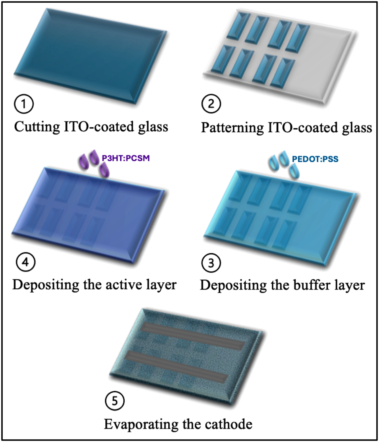
Polymer:fullerene OSCs fabrication steps.
Annealing treatments
The annealing treatments were carried out inside a nitrogen glove box at temperatures of 100, 120, 140, and 160 °C for 30 minutes, with the films or devices placed directly on a calibrated digital hotplate. In the case of film annealing (pre-annealing), thermal treatment was applied prior to cathode deposition, whereas device annealing (post-annealing) was performed after the cathode layer was deposited. Following each annealing step, the films and devices were allowed to cool to ambient temperature while resting on a metal stage to ensure uniform thermal dissipation.
Measurements and characterizations
The organic solar cell devices were characterized under ambient conditions using a xenon-lamp solar simulator (Oriel Instruments) equipped with an AM 1.5G filter. The illumination intensity was calibrated to 100 mW cm−2 using an LI-250 light meter (Bioscience) to ensure accurate and reproducible measurement conditions. Current–voltage (J–V) characteristics were recorded using a Keithley 2400 electrometer. The corresponding device architecture and layer sequence are illustrated in Figure 5.
The actual device layers.
For the spectroscopic and microscopic analyses, the P3HT:PCBM active-layer blends were spin-coated onto clean glass substrates. Optical absorption spectra were recorded using a UV–Vis spectrophotometer (PerkinElmer LAMBDA 650), while the surface morphology was examined using a field-emission scanning electron microscope (FEG-SEM, Hitachi S-4700) and an atomic force microscope (AFM, NanoInk DPN 500, scanning mode).
Procedures, results, and discussions
Annealing timing and temperature
To investigate the effects of pre-annealing and post-annealing on the performance of the polymer:fullerene solar cells, an active-layer solution of P3HT (10 mg ml−1) was prepared and spin-coated at 1000 rpm onto PEDOT:PSS/ITO-coated glass substrates. Both films and fully fabricated devices were then thermally annealed at 100 °C for 30 minutes. The influence of annealing on the optical properties of the P3HT:PCBM films was evaluated using UV–Vis spectroscopy, as shown in Figure 6. A noticeable enhancement in film absorbance—up to approximately 12%—was observed after thermal annealing, indicating improved molecular ordering and stronger optical absorption.
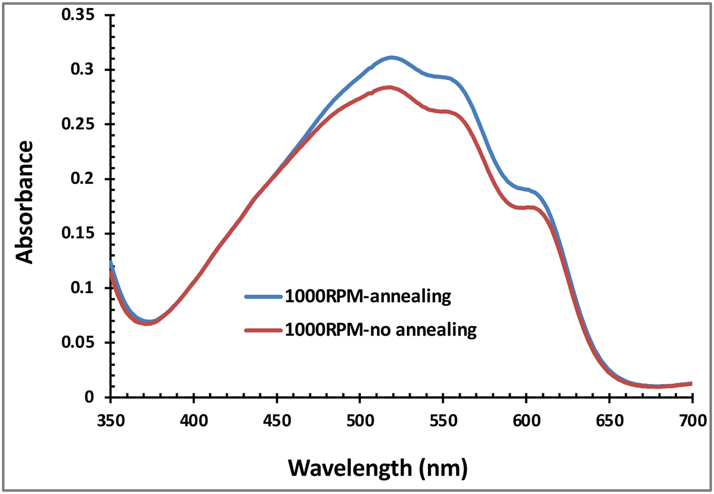
The absorbance spectra for P3HT:PCBM film spin-coated at 1000 rpm before and after annealing for 30 minutes at 100 °C.
The current–voltage characteristics (Figure 7 and Table 1) reveal that post-annealed devices exhibit substantially higher performance than their pre-annealed counterparts, with increases of approximately 26% in JSC and 38% in PCE. This superior enhancement in post-annealed devices indicates that annealing after cathode deposition more effectively improves interfacial contact, thereby promoting more efficient charge generation, extraction, and collection. It should be noted that the overall PCE remained relatively low, primarily due to partial thermal degradation during air exposure when transferring the substrates to the evaporator. In addition, the devices were not encapsulated during J–V measurements, which further contributed to performance losses (Fallata et al., 2021; Krebsa et al., 2004, 2005).
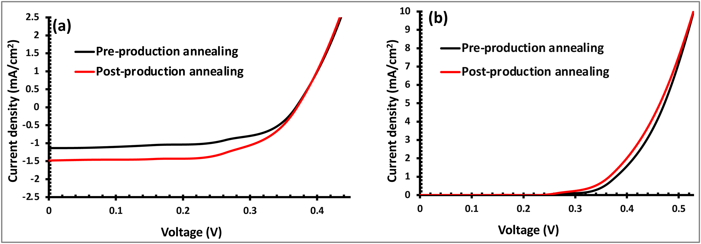
Current–voltage characteristics of pre- and post-annealed devices spin-coated at 1000 rpm: (a) under illumination and (b) in dark conditions. Devices were annealed at 100 °C for 30 minutes.
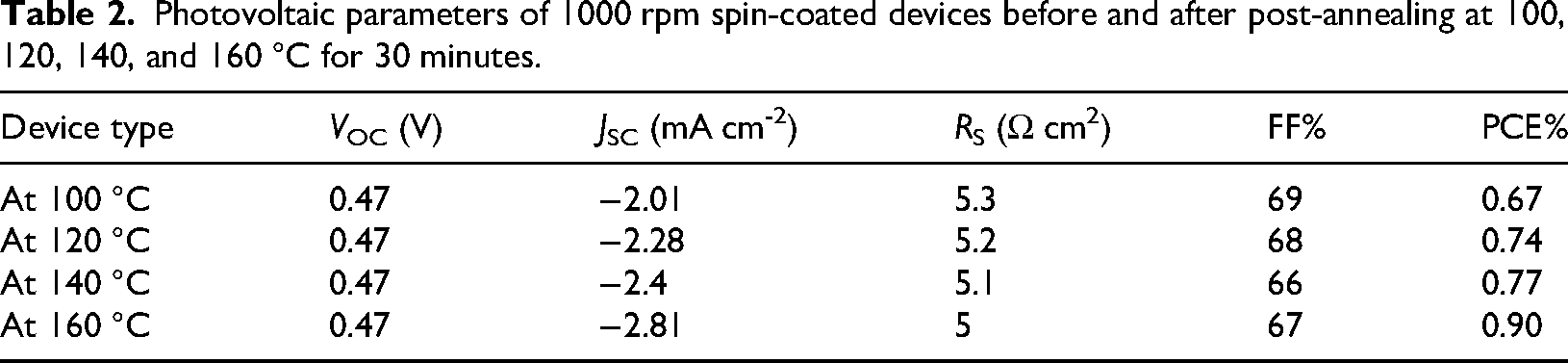
Photovoltaic parameters of 1000 rpm spin-coated devices pre- and post-annealing at 100 °C for 30 minutes.
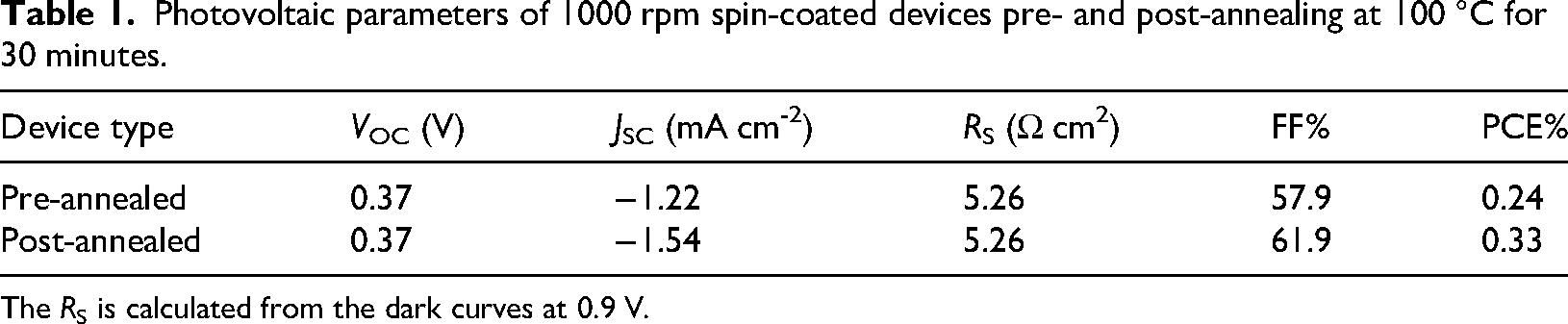
The RS is calculated from the dark curves at 0.9 V.
Several reported studies have similarly demonstrated improvements in optical absorption and photovoltaic performance following thermal annealing. Annealing promotes increased surface roughness and enhanced molecular packing within the P3HT domains, leading to a more defined nanoscale interpenetrating network between the polymer and fullerene phases. Additionally, thermal treatment improves the interfacial contact between the active layer and the cathode, with the associated increase in interfacial roughness facilitating more efficient charge extraction (Chen et al., 2009; Kim et al., 2005; Ma et al., 2005).
A new set of devices was fabricated and post-annealed at 100, 120, 140, and 160 °C for 30 minutes each. An increase in both JSC (from 2 to 2.8 mA cm−2) and PCE (from 0.66% to 0.9%) was observed, while the VOC remained largely unchanged. The FF was consistently high, ranging from 69% at 100 °C to 67% at 160 °C, among the highest values reported for this system (Kadem et al., 2016; Shaban et al., 2021). These results are summarized in Table 2, and the corresponding J–V characteristics under illumination and in the dark are shown in Figure 8. Analysis of the RS calculated from the inverse slope of the dark J–V curve at 0.9 V—revealed that increasing the annealing temperature reduces RS, which, according to Equation (1), accounts for the observed enhancement in JSC and overall device efficiency.
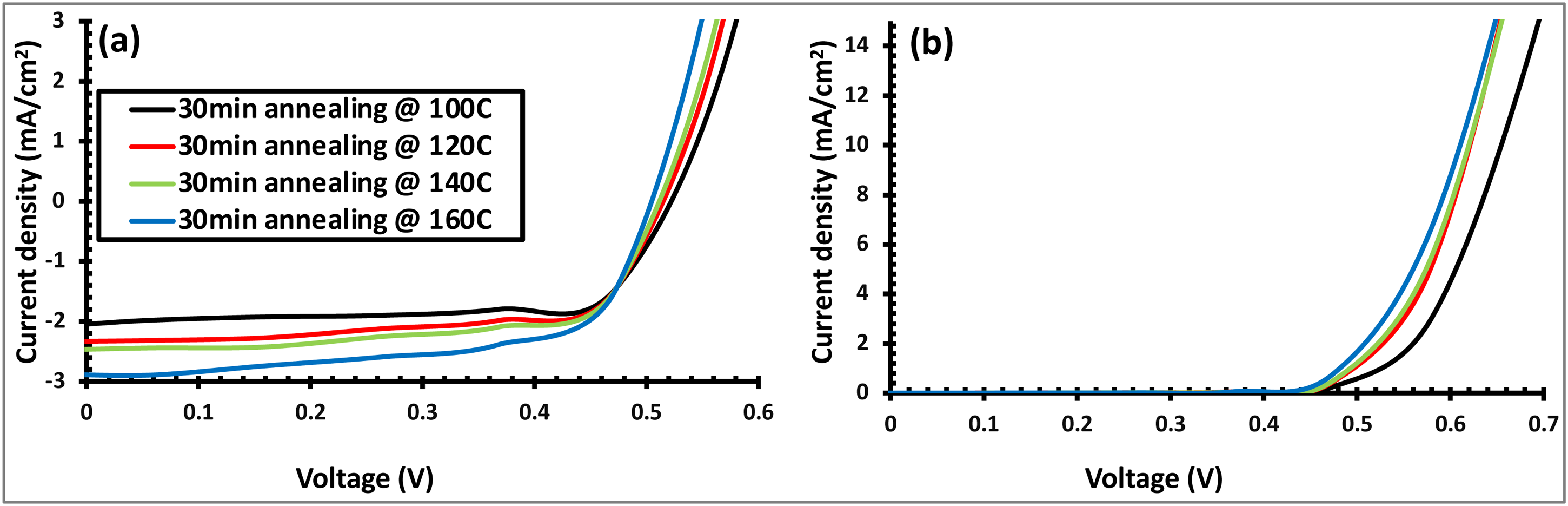
Current–voltage characteristics of post-annealed devices spin-coated at 1000 rpm: (a) under illumination and (b) in dark conditions. Devices were annealed at 100, 120, 140, and 160 °C for 30 minutes.
Photovoltaic parameters of 1000 rpm spin-coated devices before and after post-annealing at 100, 120, 140, and 160 °C for 30 minutes.
Active layer thickness
The thickness of the active layer was increased using two approaches: (a) increasing the polymer concentration in the P3HT:PCBM solution and (b) reducing the spin-coating speed (rpm). In the first approach, an active-layer solution with a double P3HT concentration (20 mg ml−1 instead of 10 mg ml−1) was prepared and spin-coated at 1000 rpm. The photovoltaic parameters of the devices after post-annealing at 160 °C for 30 minutes are summarized in Table 3. Compared to devices with the lower-concentration active layer, the VOC, JSC, FF, and PCE increased by factors of 1.26, 3.1, 1.19, and 4.07, respectively. Figure 10 presents AFM images comparing thick and thin P3HT:PCBM films spin-coated on glass substrates.
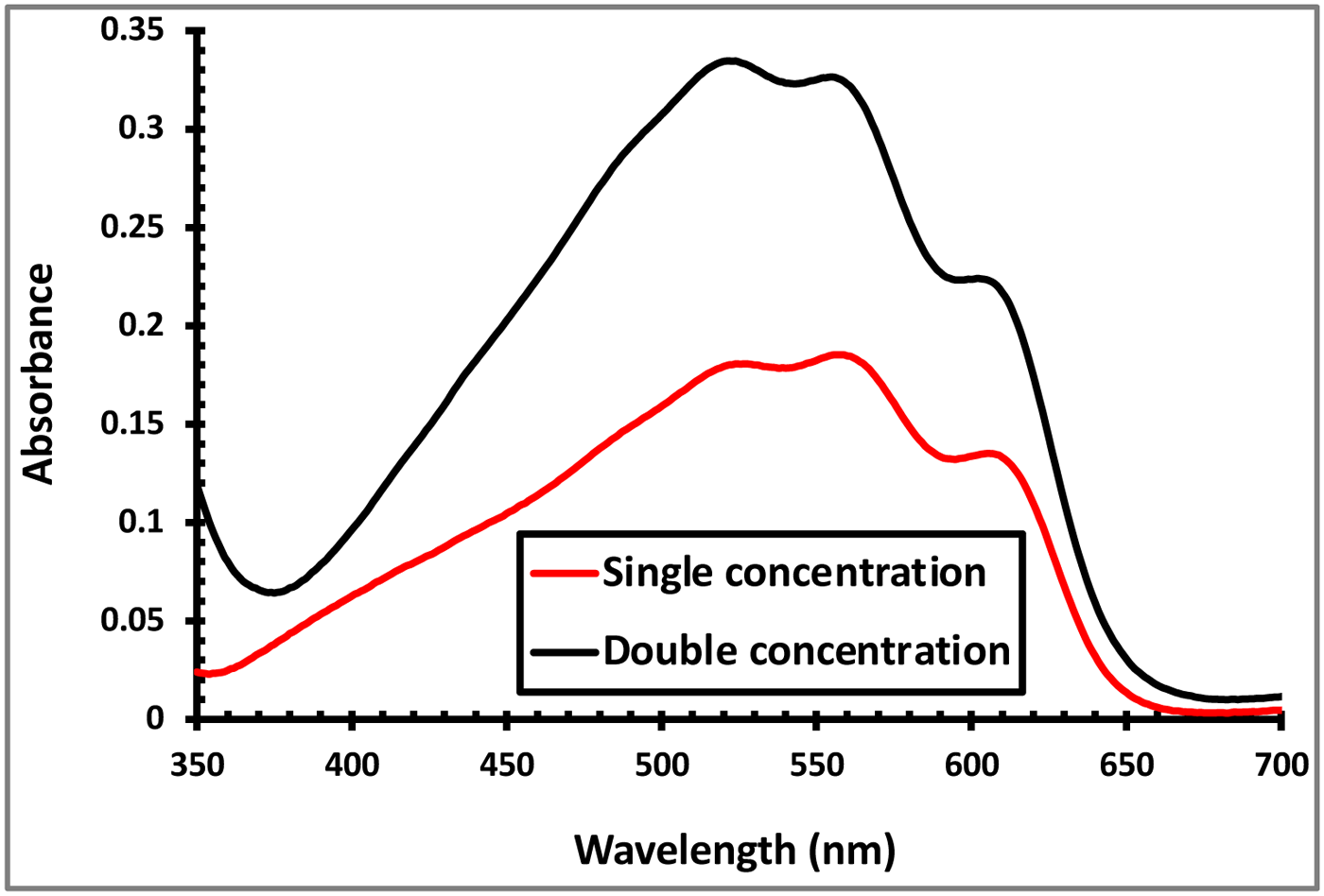
The optical absorbance of the active film with single and double concentrations of polymer in the active-layer solutions that were spun at 1000 rpm.
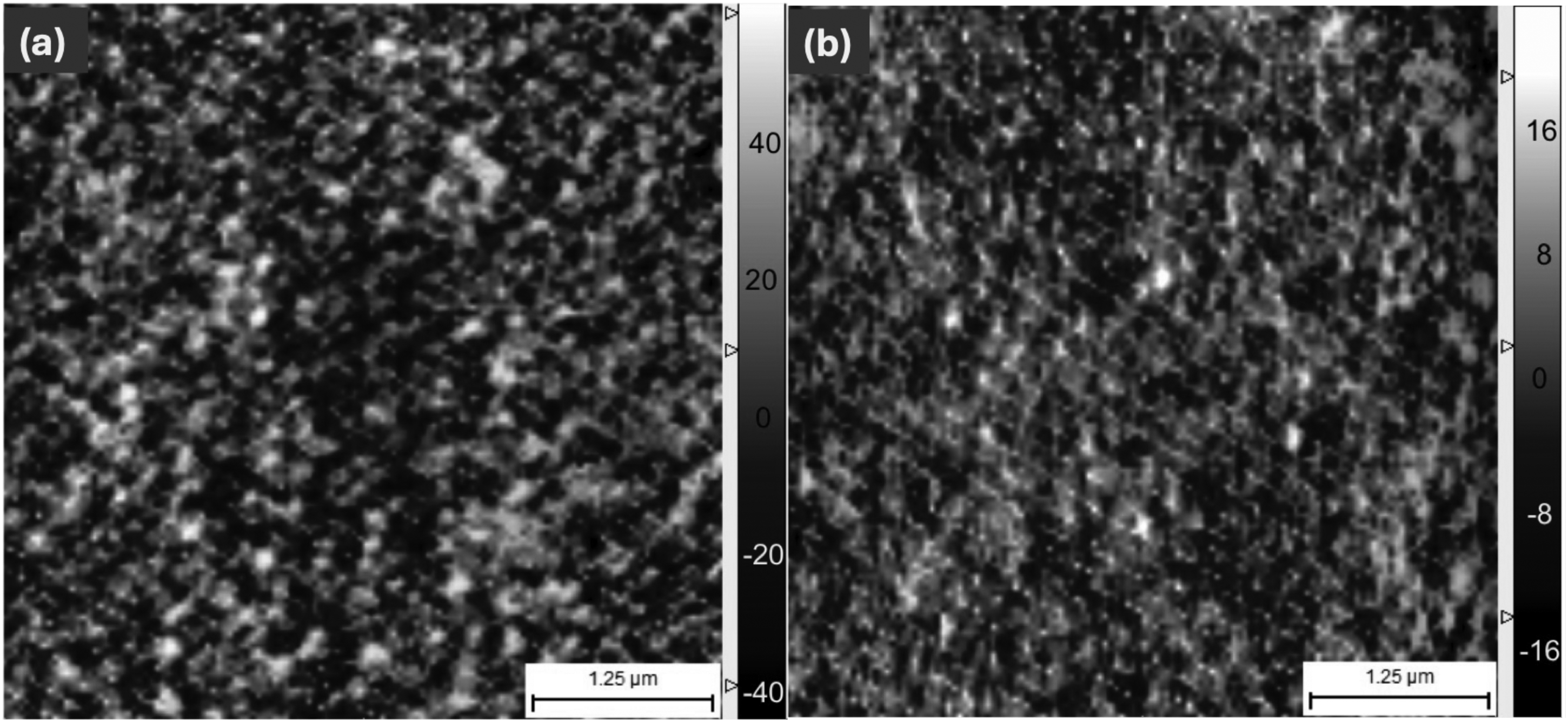
AFM micrographs for (a) thick P3HT:PCBM film (double concentration); (b) thin P3HT:PCBM film (single concentration). The bars indicate 1.25 μm.
Photovoltaic parameters for OSC devices with single and double concentrations of P3HT in the active layer.
The films were spun at 1000 rpm, and devices were post-annealed at 160 °C for 30 minutes.
The significant improvement in all photovoltaic parameters for the double-concentration active-layer devices is primarily attributed to the enhanced optical absorbance of the thicker films. Increasing the film thickness allows more incident photons to be absorbed, generating a higher number of excitons and consequently improving JSC, FF, and PCE. As shown in Figure 9, the optical absorbance of the thicker film increased by up to 97% compared to the single-concentration film. AFM micrographs in Figure 10 further illustrate the difference in surface morphology between a thick P3HT:PCBM film (double concentration) and a thin film (single concentration), both spin-coated at 1000 rpm.
This prompted an investigation into the critical active-layer thickness beyond which further increases might no longer improve the PCE. To explore this, another set of devices was fabricated using the same double-concentration solution (20 mg ml−1 P3HT), with films spin-coated at two different speeds: 1000 and 600 rpm, followed by post-annealing at 160 °C for 30 minutes. Reducing the spin-coating speed increased the film thickness from 80 nm to 100 nm, as revealed by Figure 10, which significantly enhanced light absorption (Figure 11). While VOC and FF remained essentially unchanged, the 600 rpm devices exhibited higher JSC (from 4.3 to 5.5 mA cm−2) and PCE (from 1.4% to 1.9%), primarily due to the approximately 91% increase in absorbance compared to the 1000 rpm films. Figure 11 presents a direct comparison of the optical absorbance of double-concentration films spin-coated at 1000 and 600 rpm.
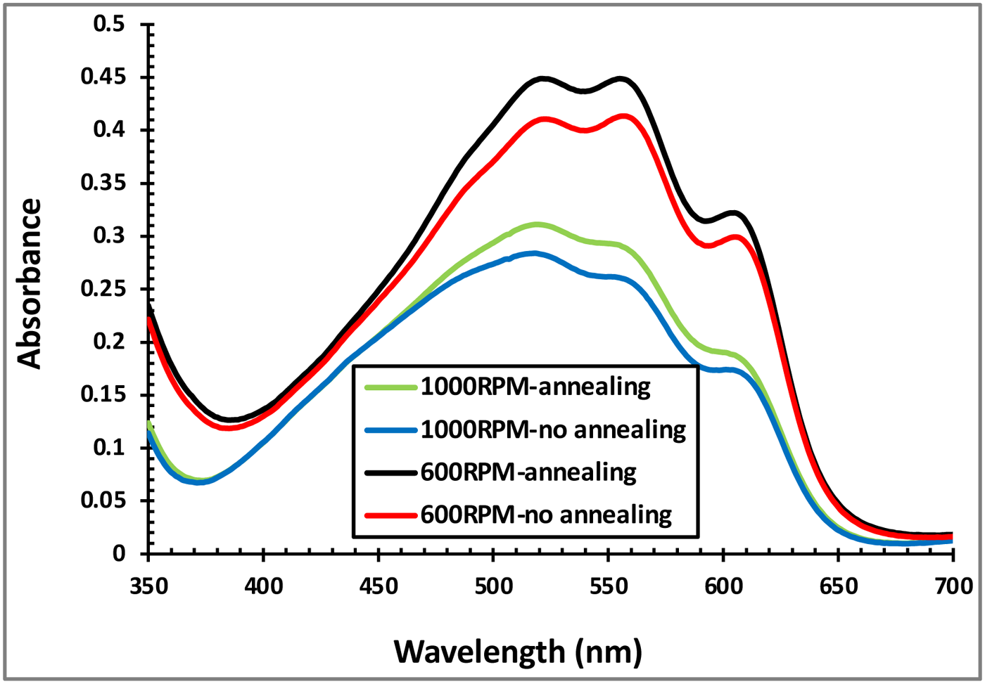
The optical absorbance of the active films with double concentrations of polymer in the active-layer solutions, which were spin-coated at 1000 and 600 rpm.
Further post-annealing was carried out at 180 °C for 10 minutes on devices that had previously undergone annealing at 160 °C for 30 minutes (i.e. a two-step annealing process, with the second step applied after the devices had cooled to ambient temperature). Under these conditions, the film spun at 1000 rpm exhibited the best overall performance. The resulting photovoltaic parameters are summarized in Table 4. For the two-step annealed devices, JSC increased to 6.6 and 6.7 mA cm−2, and PCE improved to 2.18% and 2.1% for the 1000 rpm and 600 rpm films, respectively. These results indicate that a two-step annealing process more effectively enhances the photovoltaic properties of the devices. Figure 12 shows the corresponding current–voltage characteristics measured in the dark and under illumination.
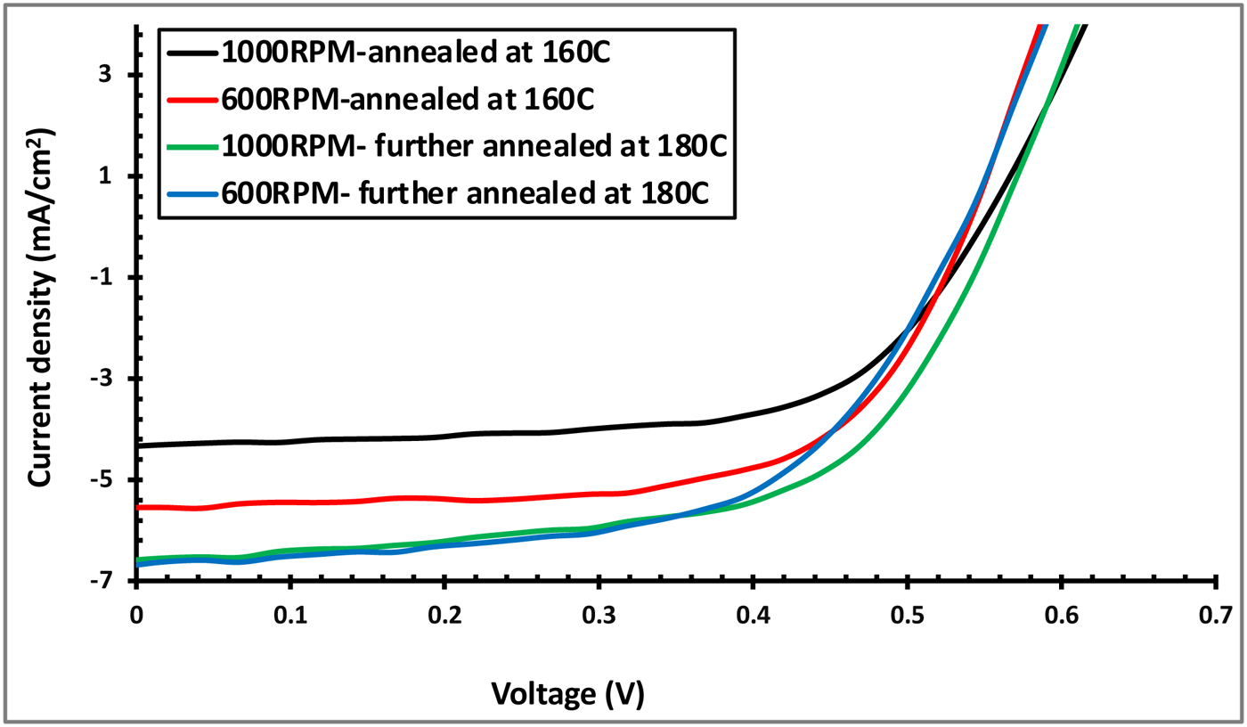
Current–voltage characteristics of devices with active layers spin-coated at 1000 and 600 rpm under illumination. Devices were post-annealed for 30 minutes at 160 °C, and for further-annealed samples, a second annealing step was performed at 180 °C for 10 minutes.
Photovoltaic parameters of double-concentration OSC devices with active layers spin-coated at 1000 and 600 rpm.
Post-annealing was performed using either a single-step or a two-step process.
Conclusion and future work
The performance of P3HT:PCBM OSCs is strongly influenced by annealing conditions, active-layer thickness, polymer concentration, and spin-coating speed. Thermal annealing enhances optical absorption and exciton generation, improving VOC, JSC, FF, and PCE, with post-annealing outperforming pre-annealing due to reduced series resistance and improved interfacial contact. Increasing the P3HT concentration from 10 to 20 mg ml−1 significantly boosted absorbance and device efficiency, with VOC, JSC, FF, and PCE increasing by factors of 1.26, 3.1, 1.19, and 4.07, respectively. Films spin-coated at 1000 rpm provided the optimal balance between thickness and charge transport, while further thickness increase via slower spin speeds enhanced JSC but had a limited impact on overall efficiency. A two-step post-annealing process—160 °C for 30 minutes followed by 180 °C for 10 minutes—produced the highest PCE (up to 2.18%) and short-circuit current, demonstrating the effectiveness of sequential thermal treatment. These findings provide clear guidelines for optimizing processing parameters to achieve high-performance P3HT:PCBM OSCs.
Future studies could explore alternative post-treatments, such as solvent vapor annealing or plasma exposure, and the incorporation of nanomaterials to further enhance light absorption, charge transport, and interfacial contact. Optimizing layer architecture, spin-coating parameters, and active-layer thickness could yield additional efficiency gains. Long-term stability and operational lifetime studies are also essential to ensure the durability of performance improvements. Coupling experimental work with device modeling may provide predictive guidance for designing high-efficiency, stable P3HT:PCBM solar cells.
Footnotes
Acknowledgement
The author acknowledges the University of Jeddah for providing the research facilities.
Ethical committee as applicable
No human participants or animals were involved research.
Contribution list
All data and explanations are done by the author.
Funding
The author received no financial support for the research, authorship, and/or publication of this article.
Declaration of conflicting interests
The author declared no potential conflicts of interest with respect to the research, authorship, and/or publication of this article.
Data availability
The author confirms that the data supporting the findings of this study are available and can be accessed within the article.