
Abstract
This article presents the performance analysis of reconfigurable multiple-switch fault-tolerant multiport DC–DC converters for renewable-based hybrid standalone applications. Detailing various switch faults, two topologies have been studied, each accompanied by a thorough exploration of operating scenarios. While the first topology is capable of addressing faults occurring in single or multiple switches, it falls short of achieving complete fault tolerance. In order to address this limitation, a fully fault-tolerant topology has been introduced, specifically designed to manage all potential combinations of multiple switch faults. To verify the efficacy of the topologies across various operating scenarios, laboratory prototypes were developed and employed. The empirical findings from real-time testing of the reconfigurable fault-tolerant topologies guarantee regulated voltage with uninterrupted supply in both charging and discharging operations of the energy storage device. The performance of the topologies related to stress, loss, reliability, and cost has also been investigated. This article also presents a comparative analysis of reconfigurable fault-tolerant converters with similar topologies.
Keywords
Introduction
In the era, where traditional energy generation and distribution are being replaced with renewable-based hybrid generation and distribution techniques, power electronic converters are playing a crucial role. The converters that interface the energy resources integrated with an energy storage device (ESD) and connected to the load are gaining popularity. The damage to the environment by traditional generation units is one of the main reasons for the new technological advancements related to renewable resources and their management. A recent guideline of the European Union suggests that carbon emissions must be reduced by about 70%–80% in the coming couple of decades. This can be made possible only by considering distributed energy resources on a large scale for the advantages they have regarding their abundant availability and zero level of harmful emissions (Abdolrasol et al., 2022; Allehyani, 2021). Therefore, significant research is being carried out to emphasize the usage of natural energy resources like solar photovoltaics (Abdolrasol et al., 2023; Singh et al., 2020); fuel cells (Das et al., 2022; Samadhiya et al., 2022; Wu et al., 2022), wind turbines, etc. (Farooq et al., 2022; Hussain et al., 2020; Singh et al., 2021). It is evident that the unpredictable power generation using some of these sources enforces the system to include an ESD such as an ESD or an ultracapacitor (Chappa et al., 2024; Latif et al., 2021; Mahafzah et al., 2022; Mishra et al., 2024). Such hybrid sources integrated into a single system have more advantages than conventional power systems like continuous supply, pollution-free, abundant availability of fuel, remote area installations, etc. In such hybrid systems, due to the continuous operation of the system, the semiconductor devices and other components undergo high stress, which leads to the failure of the respective component. This results in either increased demand on other sources or a shutdown of the complete system. In this context, the creation of systems impervious to faults becomes imperative to ensure continuous generation and heightened reliability of the overall system.
The block diagram representing the flow of operation in a fault-tolerant DC–DC converter is depicted in Figure 1. The process involves two stages, that is, fault-diagnosis and fault-compensation. The fault diagnosis is the stage of detecting the faults and its location. Fault compensation is the stage of implementing the corresponding switching strategy to continue the operation of topology similar to prefault without interruption in power supply.
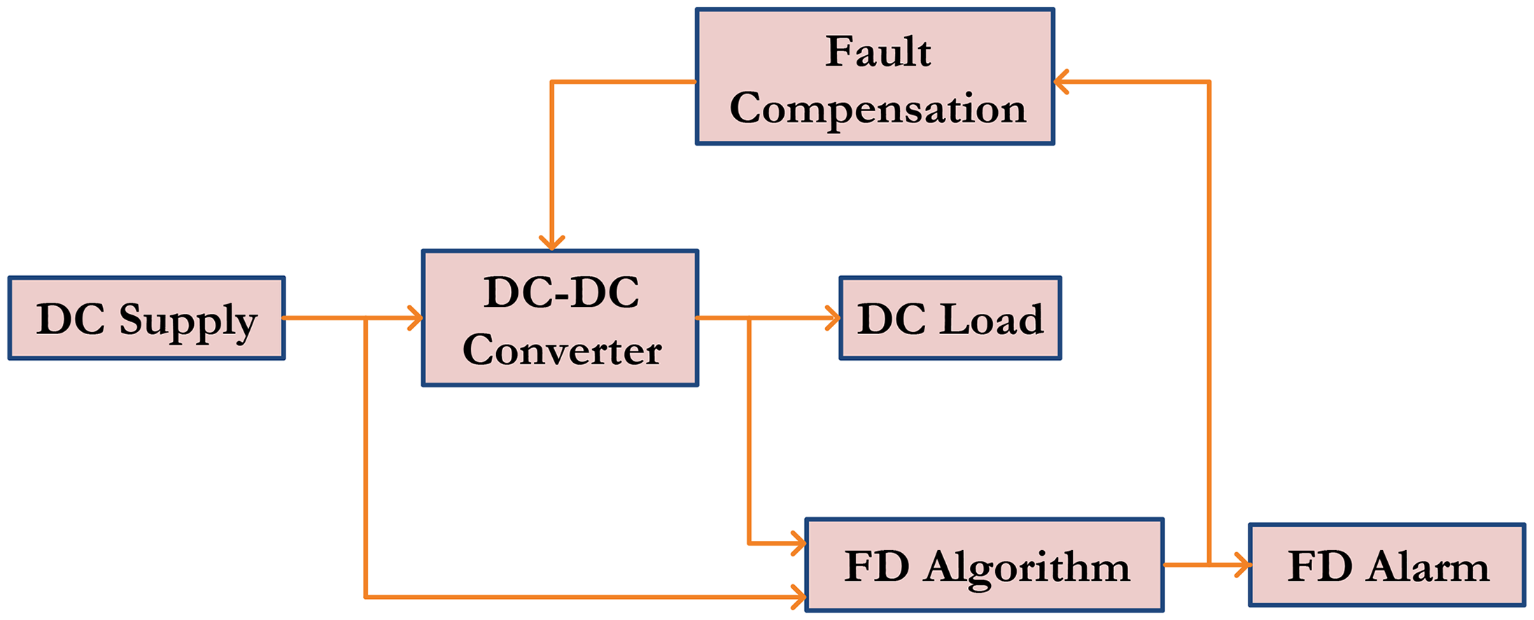
Block diagram representing the operation of fault-tolerant converter.
Mostly, the faults that occur in such systems lead to the failure of the converter's normal operation. Generally, a DC–DC converter is susceptible to various types of component failures. Among these, semiconductor device faults and capacitor faults stand out as the most prominent. According to Kumar and Elangovan (2020), nearly 34% of faults among the various components in a topology are attributed to semiconductor devices. This is primarily due to heightened stress during the energy conversion process. These faults are mainly classified into Open Circuit (OC) Faults and Short Circuit (SC) Faults. The primary cause of Open Circuit Failure (OCF) in a semiconductor device is driver failures, while Short Circuit Failure (SCF) typically arises from either overstress or excessive usage of switches (Khan and Wen, 2021).
This work presents the performance analysis of two innovative fault-tolerant topologies that are capable of addressing single and multiple-switch faults, thereby mitigating the limitations such as multiple switch fault-tolerance, regulated voltage during postfault operation, uninterrupted power supply, ability to handle both OC and SC faults, more components for reconfiguration, etc. (Ahmad et al., 2021; Emamalipour and Lam, 2022; Huang et al., 2021; Razani and Mohamed, 2021; Siouane et al., 2019; Soon et al., 2020; Wang et al., 2021; Xu et al., 2021).
The presented topologies hold applicability across various domains, including DC microgrids, alternative energy harvesting systems, standalone power plants for domestic loads, and more. Several fault detection algorithms have been reported, leveraging current and voltage sensor data (Bento and Cardoso, 2019; Kim et al., 2019; Zhuang et al., 2021). Consequently, this article's focus is solely on multiple switch fault-tolerant operations and their performance evaluation using various attributes, excluding fault detection. In general, attributes such as stress, losses, reliability, and cost analysis contribute to assessing the performance of converters. Effective maintenance of converter components to operate with minimum stress and losses improves the life of the converter. Proper design of fault-tolerance switching sequence also ensures better reliability of the converters. These performance indices help in sorting the feasibility of the converter being operated for certain applications as per demand. Many fault-tolerant converters proposed have been validated with respect to regulated and stable outputs. However, a combined study of advantages and limitations with respect to performance attributes will help in determining the superiority of converters for any specific application.
The study and analysis in this article have been organized as follows: the fault-tolerant topologies section discusses the operation of the two fault-tolerant topologies with respect to different scenarios of single and multiple switch faults, followed by validation through experimental results with detailed analysis in the results and discussion section. The performance analysis, including stress, losses, reliability, sensitivity and cost, has been discussed in the performance analysis of fault-tolerant topologies section. A quantitative comparison has been presented in the comparative analysis section, followed by the concluding remarks in the conclusion section.
Fault-tolerant topologies
The conventional power conversion system with an ESD for renewable energy applications consists of a two-stage converter (boost and charging/discharging DC–DC converter). To make this OC fault tolerant on a single switch, the diode is relocated as discussed in (Kim et al., 2019). However, the topology discussed cannot handle multiple switches and SC faults. In this regard, two fault-tolerant topologies have been presented in this section that can handle multiple switch faults and both OC and SC switch faults.
Fault-tolerant topology-I
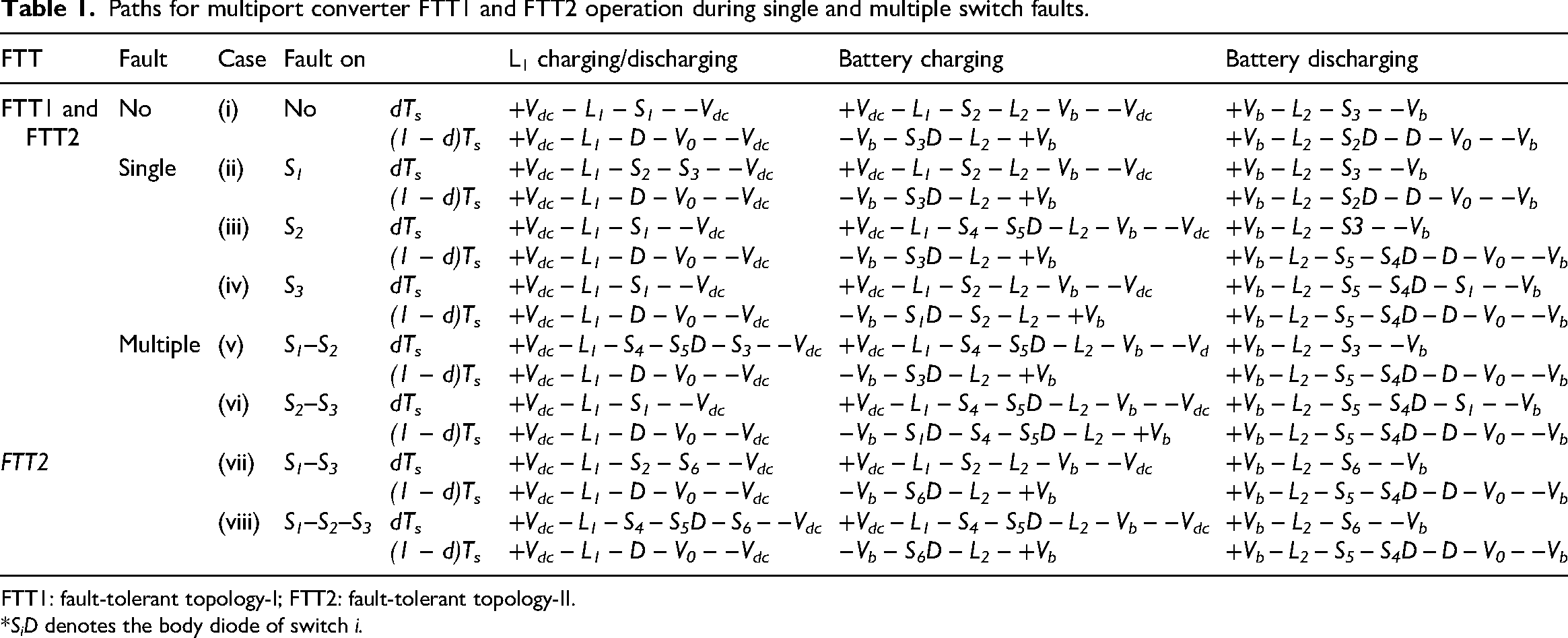
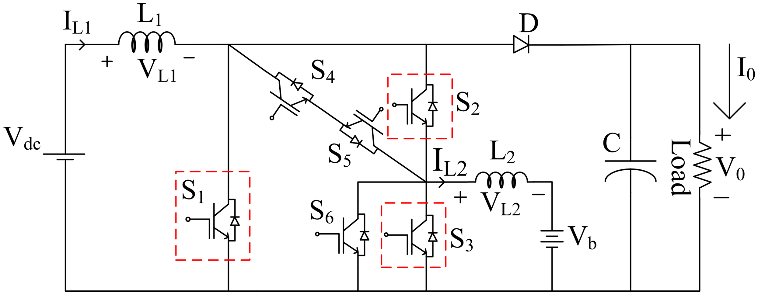
A fault-tolerant topology-I (FTT1) is presented in Figure 2 that can be incorporated in renewable energy-based hybrid systems (Pedapati and Chander, 2022). The system topology comprises a boost converter and a bidirectional converter for ESD charging/discharging. Components S1, L1, and D configure the boost converter, and S2, S3, and L2 for bidirectional conversion. S4 and S5 serve as bidirectional switches for fault tolerance. This design ensures robust ESD protection with integrated fault-tolerant features. The switching sequence of FTT1 for various fault cases is shown in Figure 3. The operating paths for simultaneous multiple switch faults on S1 and S2 and S2 and S3 have been depicted in Table 1. In the scenario where a fault occurs on switches S1 and S3, it's important to highlight a significant limitation of the current topology: the inability to reconfigure the return path for boost operation using any of the existing switches. This limitation underscores the topology's incompleteness in terms of fault tolerance. To tackle this challenge, a novel topology has been presented in the following section, aiming to surmount this particular limitation.
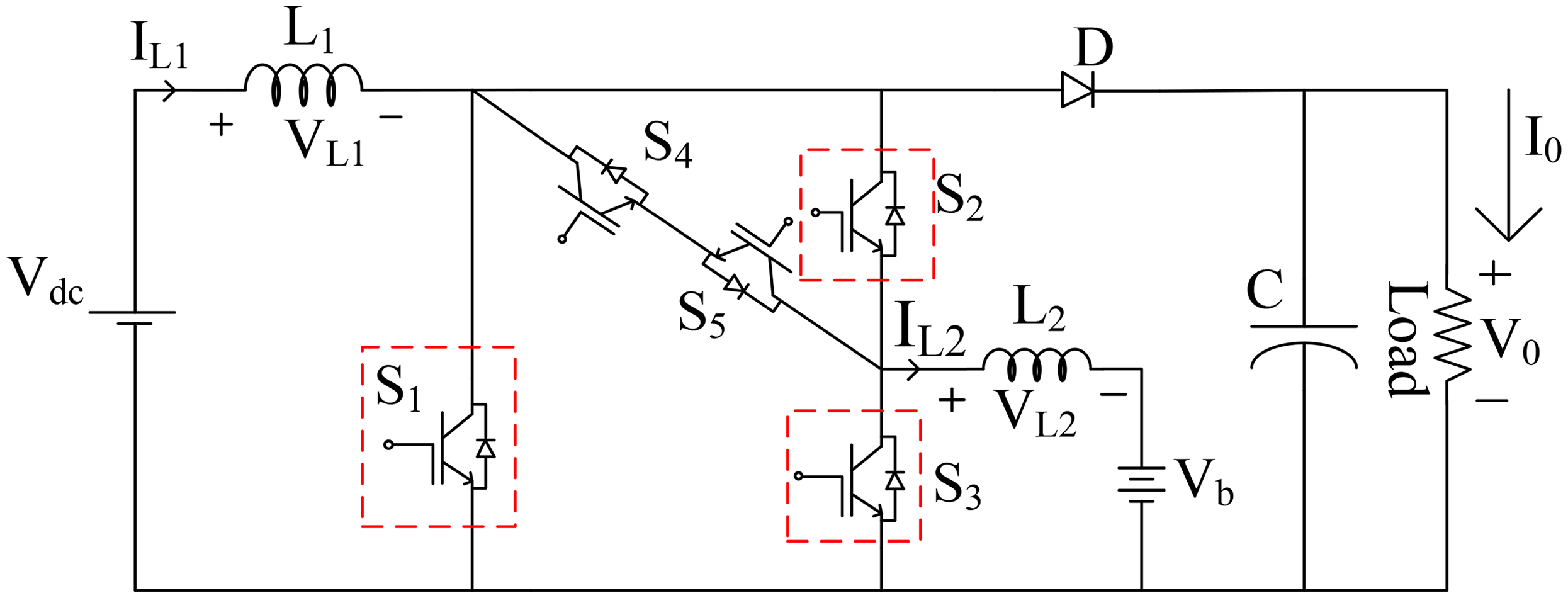
Schematic of FTT1 (Pedapati and Chander, 2022).
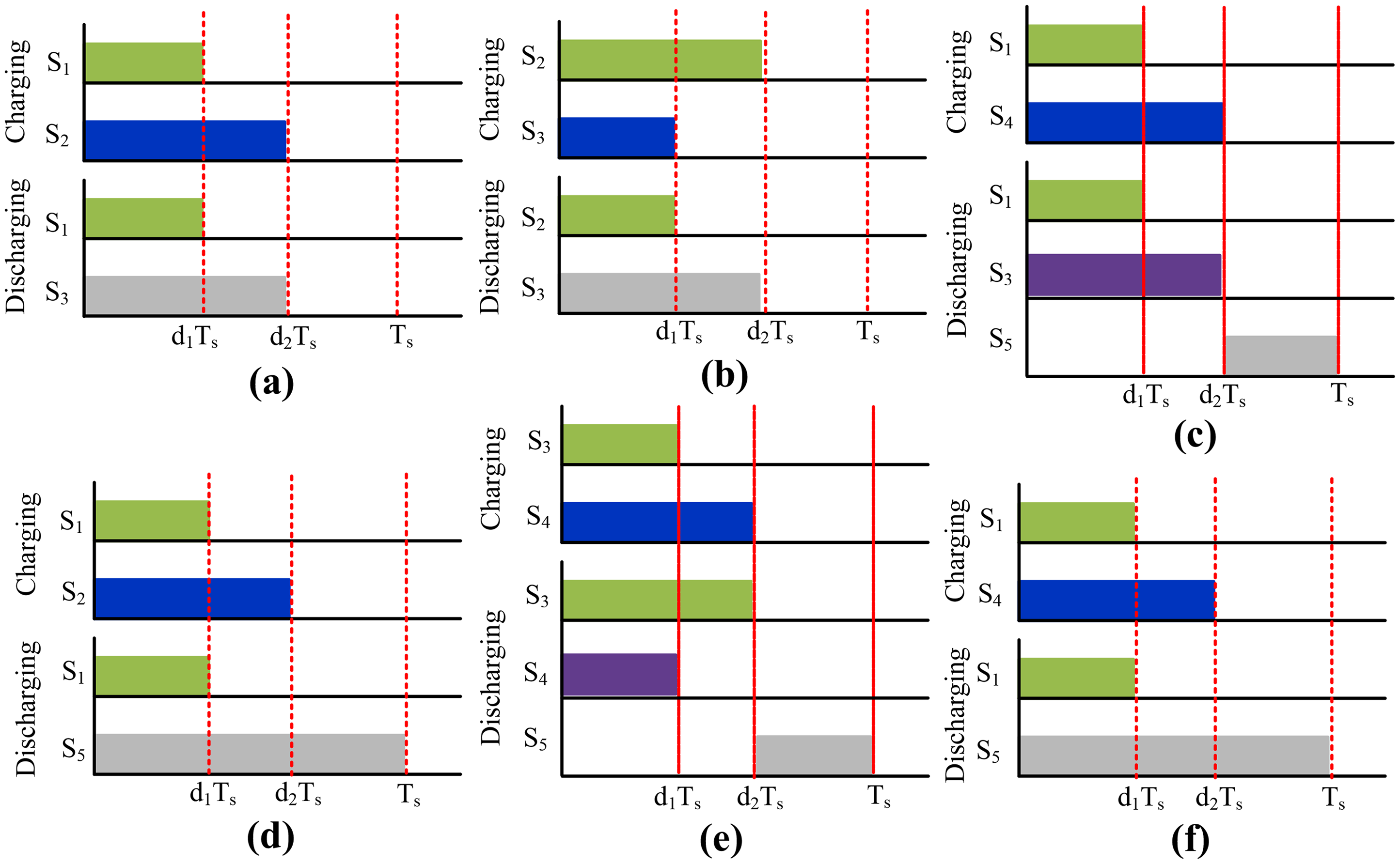
Switching sequence of FTT1 (a) Normal condition (b) Switch fault—S1 (c) Switch fault—S2 (d) Switch fault—S3 (e) Simultaneous switch fault—S1–S2 (f) Simultaneous switch fault—S2–S3.
Paths for multiport converter FTT1 and FTT2 operation during single and multiple switch faults.
FTT1: fault-tolerant topology-I; FTT2: fault-tolerant topology-II.
*SiD denotes the body diode of switch i.
Fault tolerant topology-II
Figure 4 illustrates the fault-tolerant topology-II (FTT2) (Pedapati and Hemachander, 2023). To enhance fault tolerance in FTT1 and address the issue of multiple switch faults occurring on switches S1 and S3 and S1, S2 and S3, an additional switch S6, is introduced in parallel to S3. This addition aims to provide redundancy and improve the system's resilience. This gives the added advantage of providing a return path under the S1–S3 fault condition, making it completely fault-tolerant. FTT2 operates similarly to the previous topology, FTT1, in handling single switch faults on S1, S2, and S3 individually, as well as multiple switch faults on S1–S2 and S2–S3. However, FTT2 also addresses other scenarios involving multiple switch faults that were not covered by FTT1. This expanded fault tolerance capability enhances the robustness of the system in various fault scenarios, ensuring reliable operation even under adverse conditions. The same has been discussed below with the help of Figure 5 and Table 1.
Schematic of FTT2 (Pedapati and Hemachander, 2023).
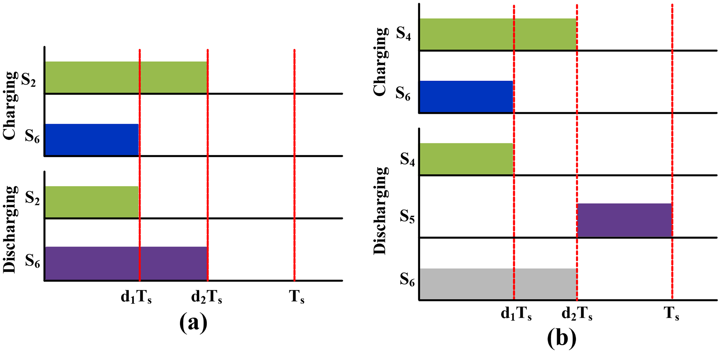
Switching diagrams of FTT2 (a) Simultaneous switch fault—S1–S3 (b) Simultaneous switch fault—S1–S2–S3.
During simultaneous fault on multiple switches S1 and S3 and S1, S2, and S3, the redundant path for boost operation is provided as shown in Figure 5(a) and (b) respectively. The operating paths for the same have been presented in Table 1. An alternate redundant path for simultaneous switch fault on S1 and S3 can also be provided through the switches S3, S4 and S5, however, at the cost of increased voltage drop. Hence, it is clear that FTT2 surpasses FTT1 due to its features such as complete fault tolerance, consistent output voltage, continuous operation, and enhanced reliability.
Steady state operation
Utilizing the switching sequence outlined in Figures 3 and 5, the steady-state analysis of the proposed FTC has been tabulated as shown in Table 2. It can be observed that the switching sequence is compensated for fault scenarios to maintain the boost mode when the ESD is idle, buck mode to charge the ESD and boost mode to discharge the ESD.
Steady state analysis for FTT1 and FTT2.
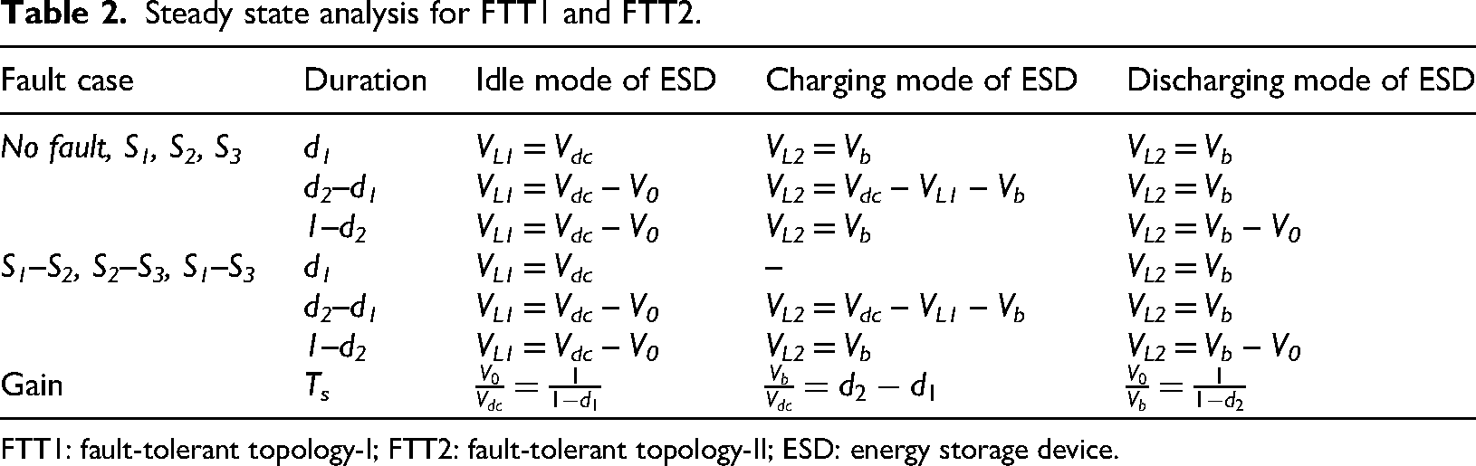
FTT1: fault-tolerant topology-I; FTT2: fault-tolerant topology-II; ESD: energy storage device.
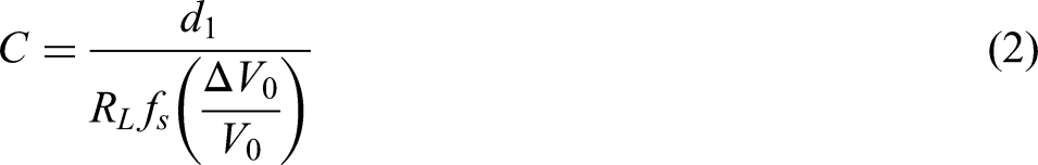
Filter components have been designed using,
Results and discussion
The performance of the fault-tolerant topologies discussed in the previous section has been validated in real-time under different operating scenarios on the developed laboratory prototype shown in Figure 6. The circuit specifications and operational parameters have been taken into account in accordance with Table 3. The controller onboard is Xilinx Spartan-6 XC6SLX9 FPGA in a TQG144 package with 90KB RAM and two clock management tiles operating at clock frequency of 100 MHz. It has 34 header pins used for SPM Interface and 40 header pins for External Interface which includes six PWM pins, 37 I/O pins, and four capture pins. A 4-channel 12-bit I2C-based ADC and 1-channel DAC are also a part of TQG144 package. The filter components were determined through equations (1) and (2) (Erickson and Robert, 2001). A rapid-response fuse is linked in series with the switches to disrupt the circuit in the event of an SC fault occurring on the switch, effectively treating it as an open-circuit fault. In case of an OC fault, the switch however acts as an open circuit. The corresponding switching sequences have been employed immediately after the switch faults so as to deliver uninterrupted output voltage. The experiments have been conducted and results have been presented for all combinations of switch faults discussed in the fault-tolerant topologies section. There have been many fault detection algorithms reported based on passive component's measurements (Bento and Cardoso, 2019; Kim et al., 2019; Zhuang et al., 2021). Hence, the focus of this article is only on fault-tolerant operations and not on fault detection. Figure 7(a) shows the real-time results of FTT1 during the transition from charging mode to discharging mode of the ESD. The topology ensures that the output voltage remains stable at 110 V during the transition from charging to the alternative ESD mode. This shift in ESD operational mode can be identified by the alteration of ESD current (IL2) from positive to negative value. The equivalent change in input current (IL1) can also be observed. The experimental results of FTT1 operating in the charging mode of ESD during a switch fault on S1 are presented in Figure 7(b). The change in ESD current can be observed as the switching strategy employed utilizes the same switch S2 for both voltage regulation and charging of ESD. During the fault on switch S2 while charging the ESD, the switching strategy employed reconfigures the circuit to provide an alternate path for the current using an auxiliary switch, and hence no major change has been observed in V0, IL1, and IL2 as shown in Figure 7(c). Figure 7(d) illustrates the experimental outcome of FTT1 in the event of a single switch fault occurring on switch S3 during the discharging phase of ESD.
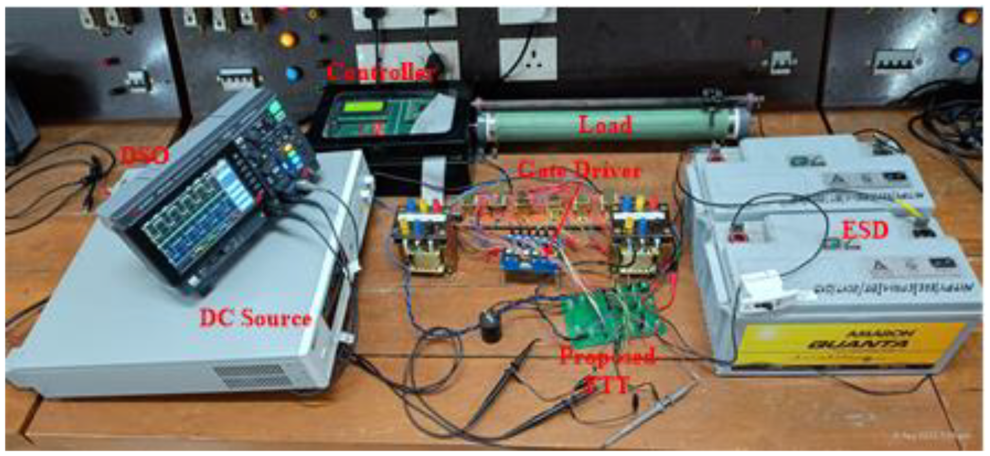
Photograph of laboratory prototype of fault-tolerant topologies.
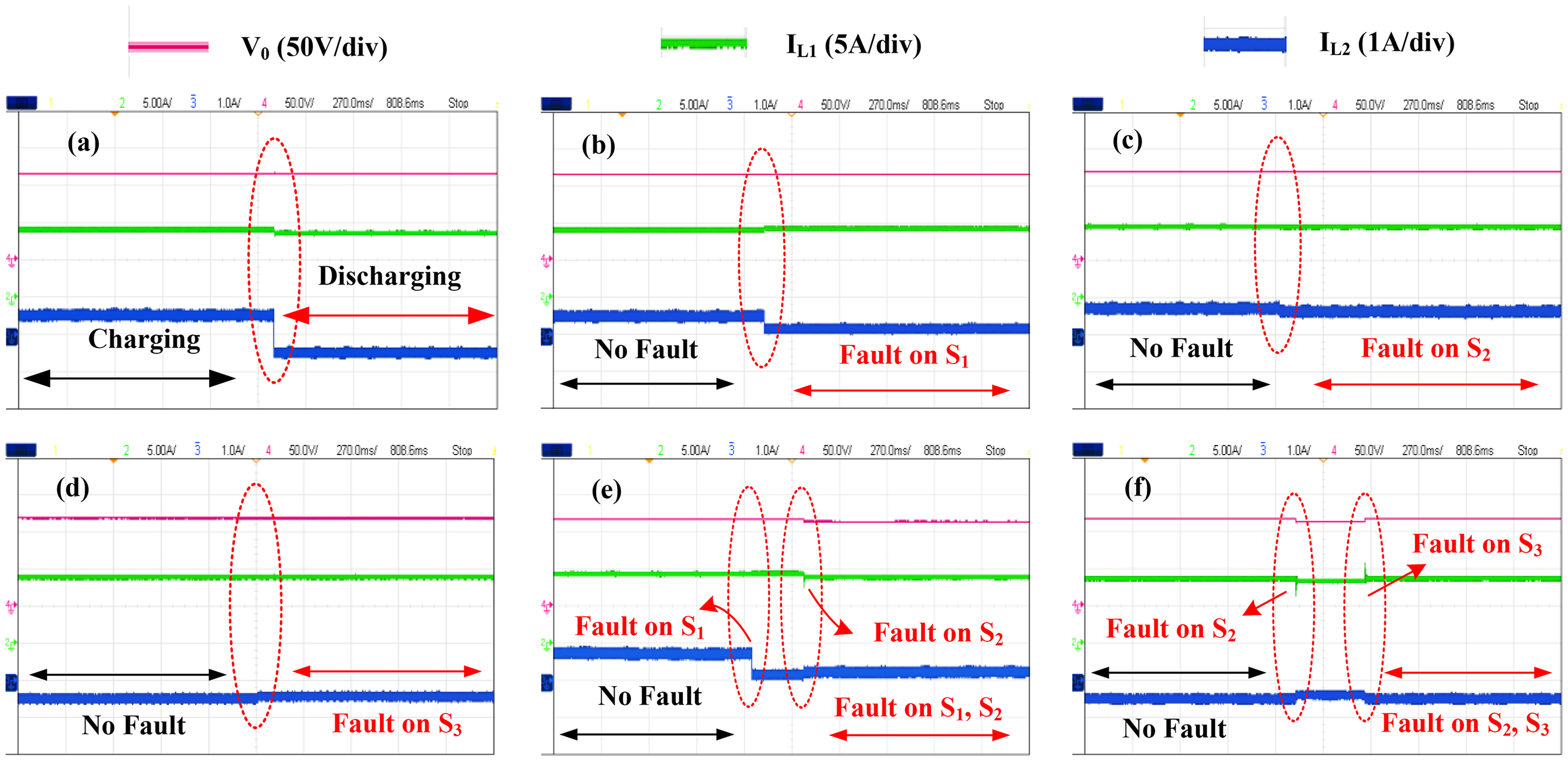
Experimental results of FTT1 (a) Charging mode to discharging mode—no-fault (b) Charging mode—fault on S1 (c) Charging mode—fault on S2 (d) Discharging mode—fault on S3 (e) Charging mode—sequential fault on S1 and S2 (f) Discharging mode—sequential fault on S2 and S3.
Specifications used for laboratory prototype.
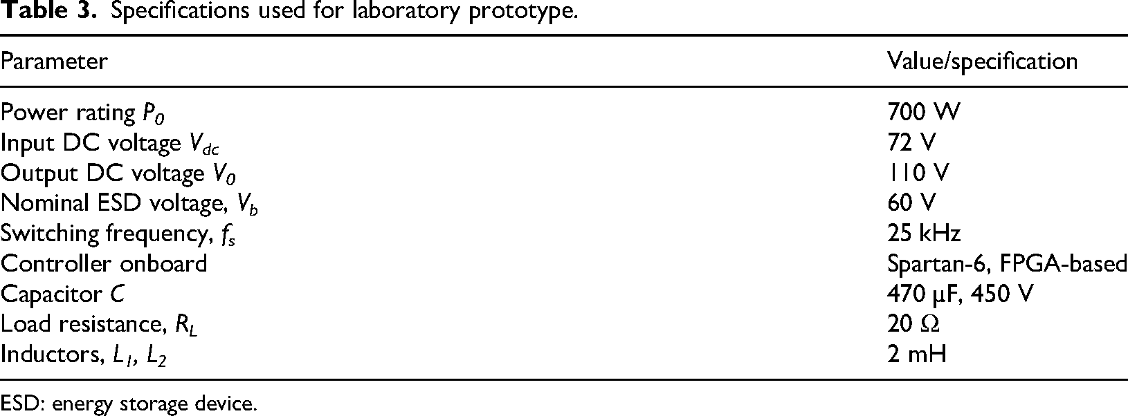
ESD: energy storage device.
The experimental results of FTT1 operated during a sequential switch fault on S1–S2 in the charging mode of ESD as shown in Figure 7(e). The result shows that the regulated load voltage is achieved with a ripple of less than 10% during postfault operation. However, it is observed that the charging current has been reduced since the switch S3 has been shared for both boost and charging operations, limiting the feasibility of maintaining different duty ratios. Similar empirical results are shown in Figure 7(f), for ESD for discharging mode during simultaneous faults on switches S2–S3.
As mentioned previously, the switching sequence utilized in FTT2 for individual switch faults on S1, S2, or S3 mirrors that of FTT1. Consequently, the outcomes obtained align closely with those depicted in Figure 7. The operating procedure of FTT2 during multiple switch faults on S1–S2 and S2–S3 is similar to that of FTT1. To overcome the limitation of FTT1 concerning the return path for multiple switch faults in switches S1 and S3, the topology has been reconfigured with a redundant switch S6. Accordingly, the experimental results presented in Figure 8(a), ensure the fault-tolerance capability of FTT2 for multiple switch faults on switches S1 and S3 occurring sequentially. The redundant switch also enables FTT2 topology to handle multiple switch faults on switches S1, S2 and S3. The same has been validated with the results presented in Figure 8(b) and 8(c) during both the charging and discharging modes of ESD, respectively. It has been observed that the output voltage is regulated for various multiple switch fault scenarios.
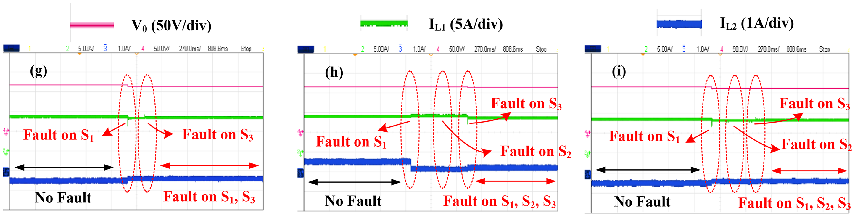
Experimental results of FTT2 (a) Discharging mode—sequential fault on S1 and S3 (b) Charging mode—sequential fault on S1, S2, and S3 (c) Discharging mode—sequential fault on S1, S2, and S3.
The findings showcased confirm the efficacy of FTT2 in managing more than one simultaneous switch fault while maintaining a regulated output voltage. This demonstrates its capability to handle various types of switch faults across both ESD operating modes, all while boasting fewer components and enhanced reliability.
Performance analysis of fault-tolerant topologies
Stress analysis
Ensuring that each switch is adequately stressed is a critical consideration when designing fault-tolerant converters. Since this article deals with the fault tolerance of switches, the stress analysis has been addressed only on the semiconductor devices considered to be under the influence of faults. Selection of suitable semiconductor devices while in the design phase will enhance the performance of the system to a greater extent. This selection is easy when the stress analysis of the converter is handy. The stress can be different depending on the state of operation of switches (on-state and off-state). This stress on switches can be classified into two types: (i) Voltage Stress and (ii) Current Stress (Sahu et al., 2019).
Voltage stress
The voltage blocked by a switch during its off-state is referred to as the voltage stress on the switch. This has been analyzed for the topologies shown in Figures 2 and 4. The maximum voltage blocked by switch S1 can be depicted as
Current and voltage stress on semiconductors of reported topologies.
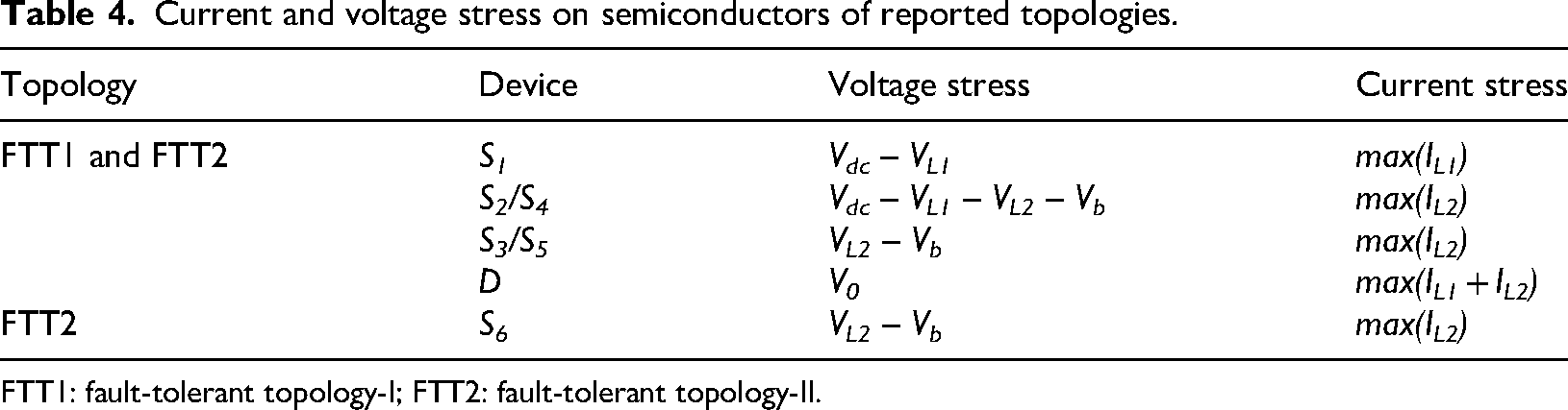
FTT1: fault-tolerant topology-I; FTT2: fault-tolerant topology-II.
Current stress
The maximum possible current passing through the switch during its on-state is referred to as the current stress on that switch. For the topologies in Figures 2 and 4, the maximum current flowing through each switch is evaluated as
Quantitative comparison of current and voltage stress on semiconductors of FTT1 and FTT2.
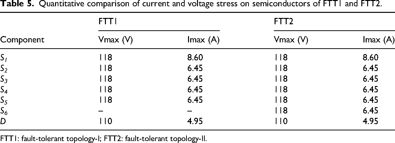
FTT1: fault-tolerant topology-I; FTT2: fault-tolerant topology-II.
Losses and efficiency
It is a well-established fact that a converter is recognized for real-time industrial implementation depending on how high the converter's efficiency can be when operated in different scenarios. Hence, the losses and efficiency analysis has been evaluated for both the topologies. In power electronic converters, a significant portion of the total loss arises from conduction and switching losses, which collectively represent the overall loss of the component (Ustun and Mekhilef, 2010). The conduction losses 


For the topologies discussed, the same has been studied and tabulated for various operating scenarios. The losses for all the components have been determined empirically, and the efficiency for both the topologies has been evaluated considering different modes of operation of ESD with respect to various switch fault case scenarios. Figure 9 presents the loss distribution analysis for all components of FTT1. The component specifications considered for this analysis are shown in Table 2. PL1 and PL2 are the losses in inductors L1 and L2, respectively, PC is the loss in the capacitor, PD is the loss in the diode, PS is the total loss in the switches. Similarly, the loss distribution analysis for FTT2 has also been shown in Figure 10. It is to be noted that the loss percentages shown in Figures 11 and 12 are the average losses considering all possible combinations of switch faults. From the losses presented, it can be observed that the average switching loss in FTT2 is increased by 4% compared to FTT1 due to the extra switch S6. In addition, it is observed that the combined passive component loss (PL1 and PL2) and filter component loss (Pc) are almost constant in both FTT1 and FTT2. Hence, it can be concluded that the complete fault-tolerant ability has been achieved by FTT2 by adding an extra switch (S6) in FTT1 without significant variation in overall loss.
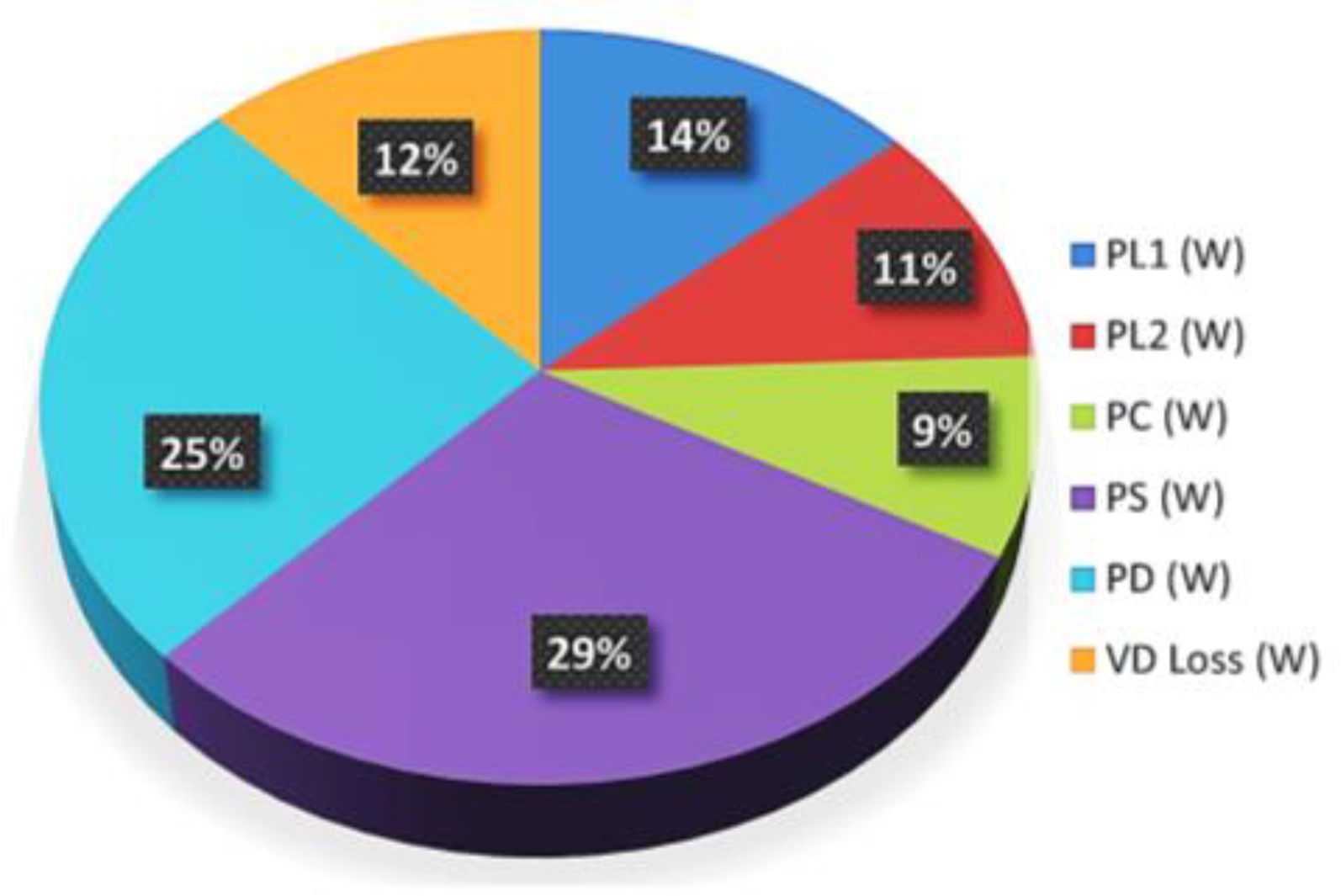
Component wise loss distribution analysis of FTT1.
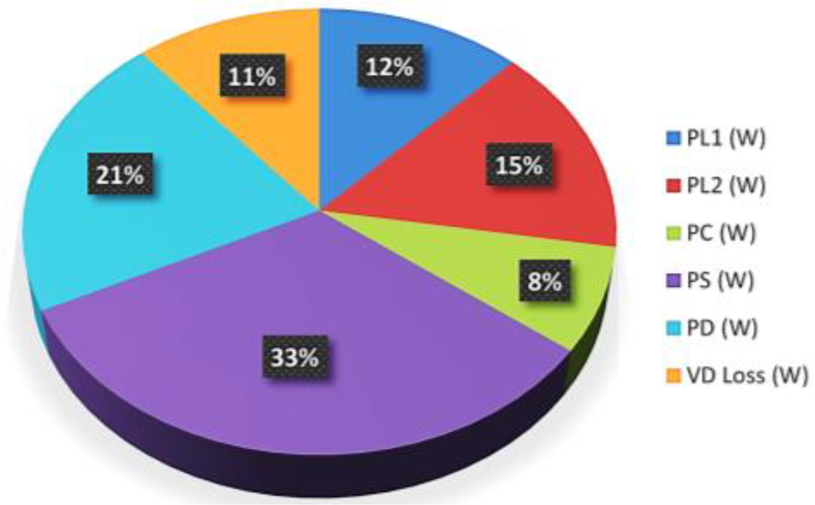
Component-wise loss distribution analysis of FTT2.
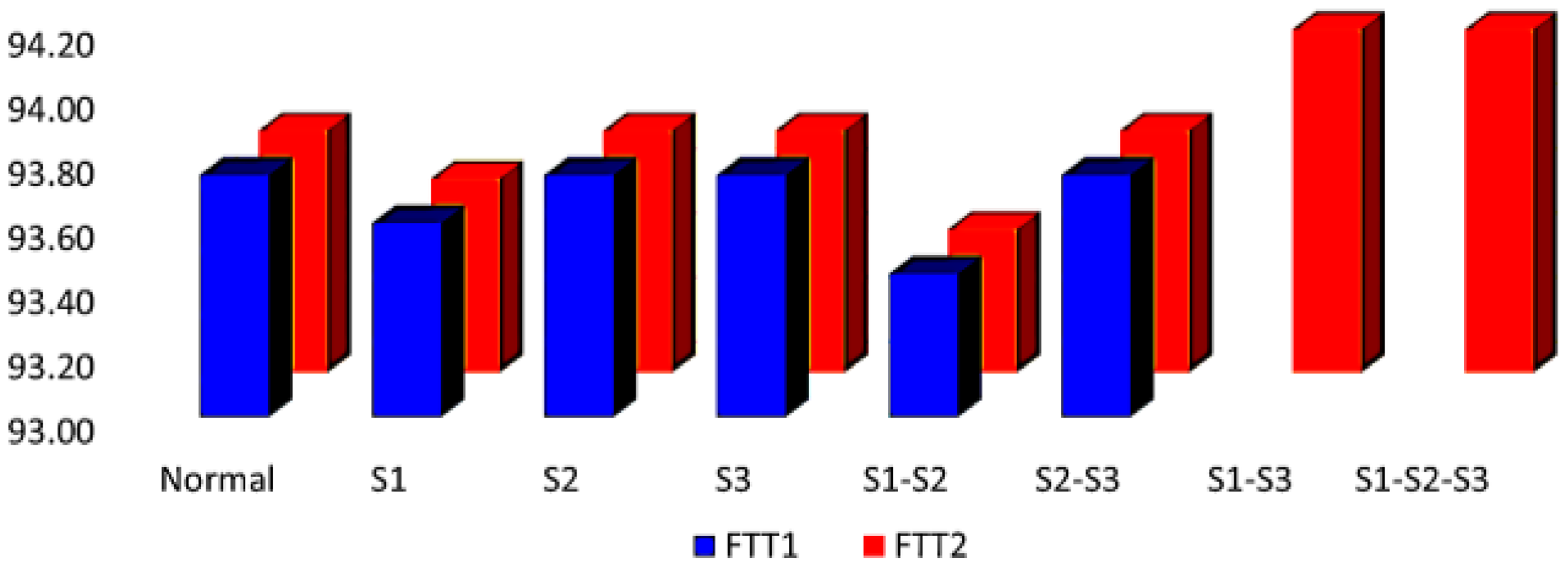
Comparison of efficiencies among the FTT1 and FTT2 during charging mode of ESD in all operating cases.
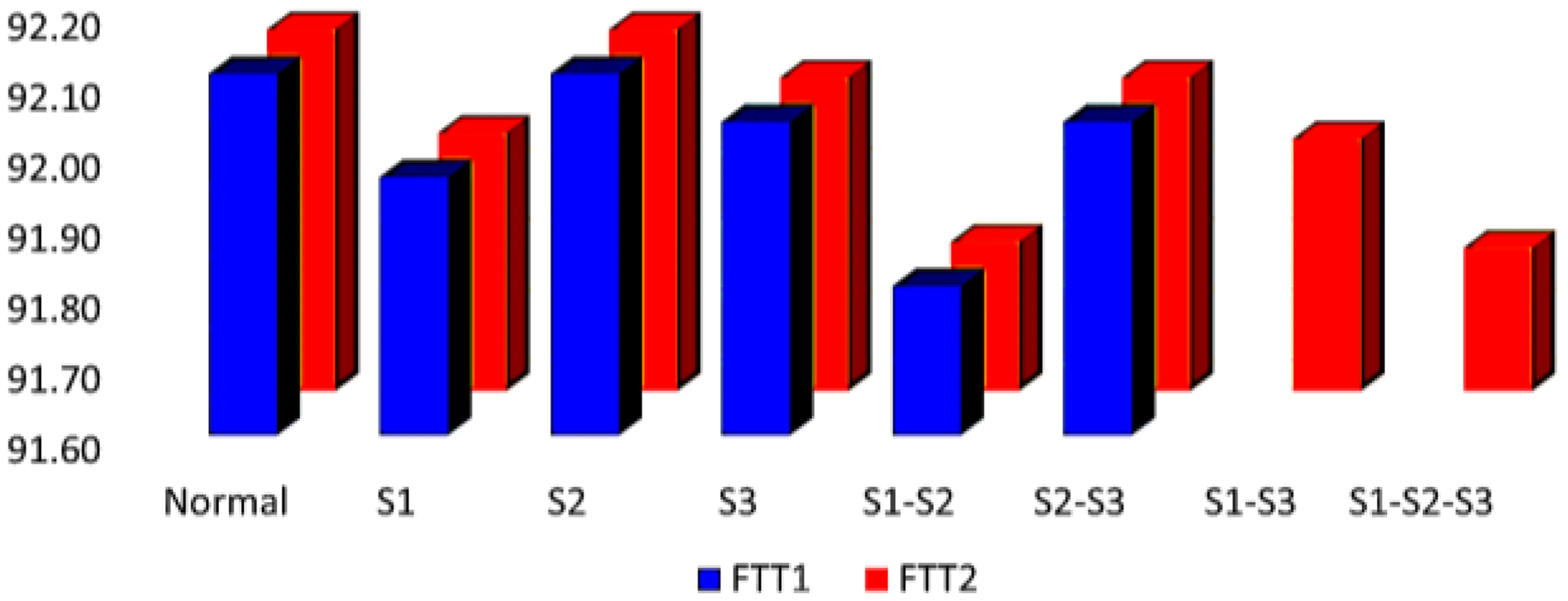
Comparison of efficiencies among the FTT1 and FTT2 during discharging mode of ESD in all operating cases.
In the loss analysis, efficiency is computed using equations (6) and (7) for charging and discharging modes of ESD, where PB is the power consumed/delivered by ESD, P0 is the output power and PIN is the input power from the source. Figures 11 and 12 display efficiency comparisons between FTT1 and FTT2 across various possible combinations of switch faults during different operating modes of ESD. It can be observed that the efficiencies of topologies FTT1 and FTT2 are same for no-fault, fault on switches S1, S2, S3, S1–S2, S2–S3 as the operating paths are same. However, as FTT1 fails to operate during S1–S3 and S1–S2–S3 switch fault scenarios, only FTT2 efficiencies have been reported.

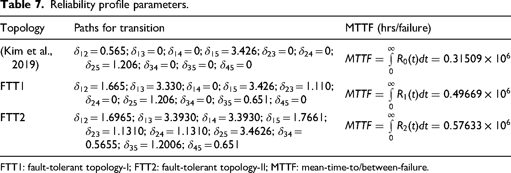
Reliability analysis
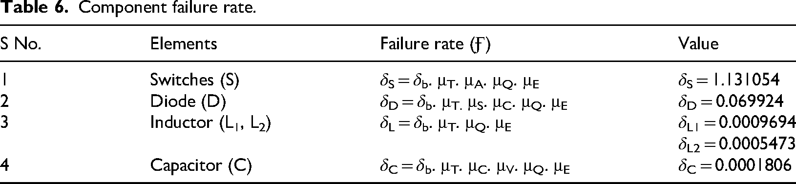
This section addresses the performance analysis with respect to reliability for the topologies, FTT1 and FTT2. The reliability analysis has been conducted utilizing the Markov Reliability Assessment Approach (MRAA) for both the established and FTTs discussed in previous sections. This approach determines the mean-time-to/between-failure (MTTF) profile of the converter by employing directed graphs to comprehend the probability of transitioning from one state to another. In this article, the states are defined by the potential number of switch faults within the topology and the directed graph is constructed to illustrate the likelihood of transitioning between various finite possibilities. Figure 13 depicts the reliability model of the Markov Chain applied to both existing and present converters, illustrating the number of switch faults across five states and ten possible state transitions. The reliability of different fault-tolerant converter topologies has been investigated using the MRAA in (Emamalipour and Lam, 2022; Kumar et al., 2022; Tarzamni et al., 2021). In this study, the reliability analysis encompasses five states: (1) Healthy: All switches and components are operational, (2) Single Switch Fault: One of the switches designated for fault tolerance experiences a fault, (3) Two Switch Fault: Two of the switches designated for fault tolerance experience faults, (4) Three Switch Fault: All switches designated for fault tolerance experience faults, (5) Absorbing: One of the redundant switches or components experiences a fault, leading to complete converter failure. The standard failure rates of each component have been assessed utilizing the military handbook MIL-HDBK-217F (n.d.). The failure rates
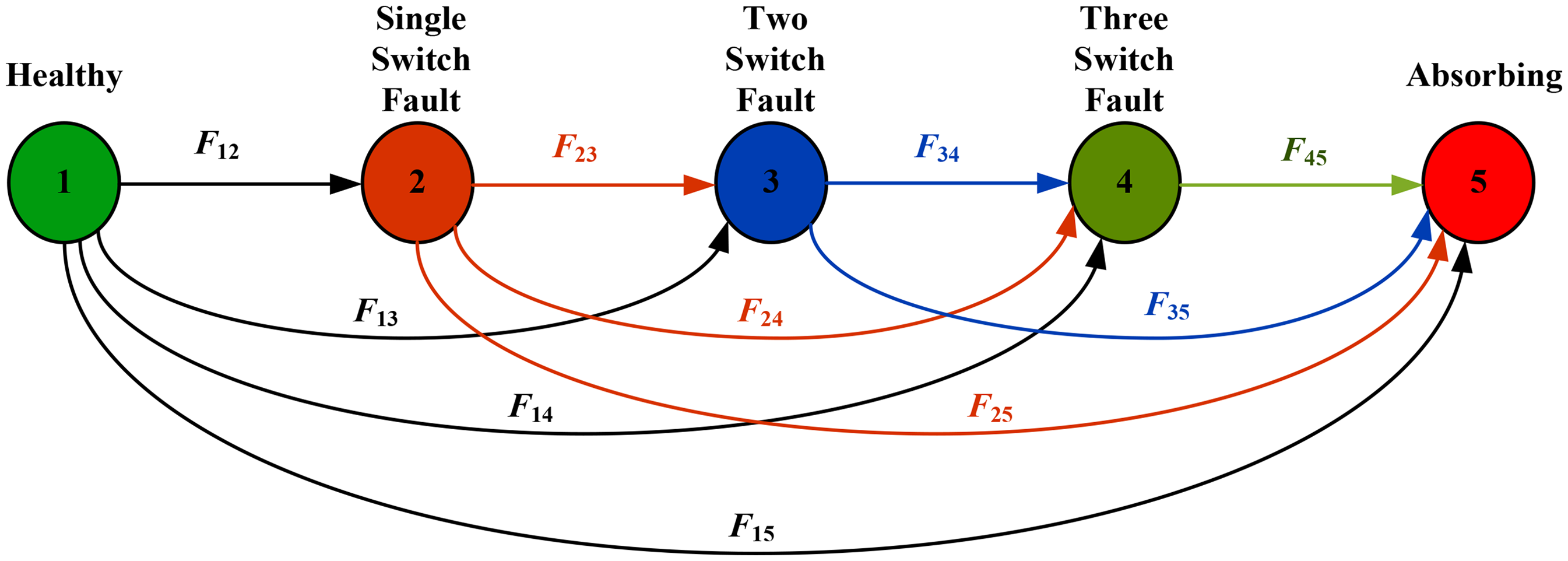
Reliability model of fault-tolerant converters based on Markov Chain.
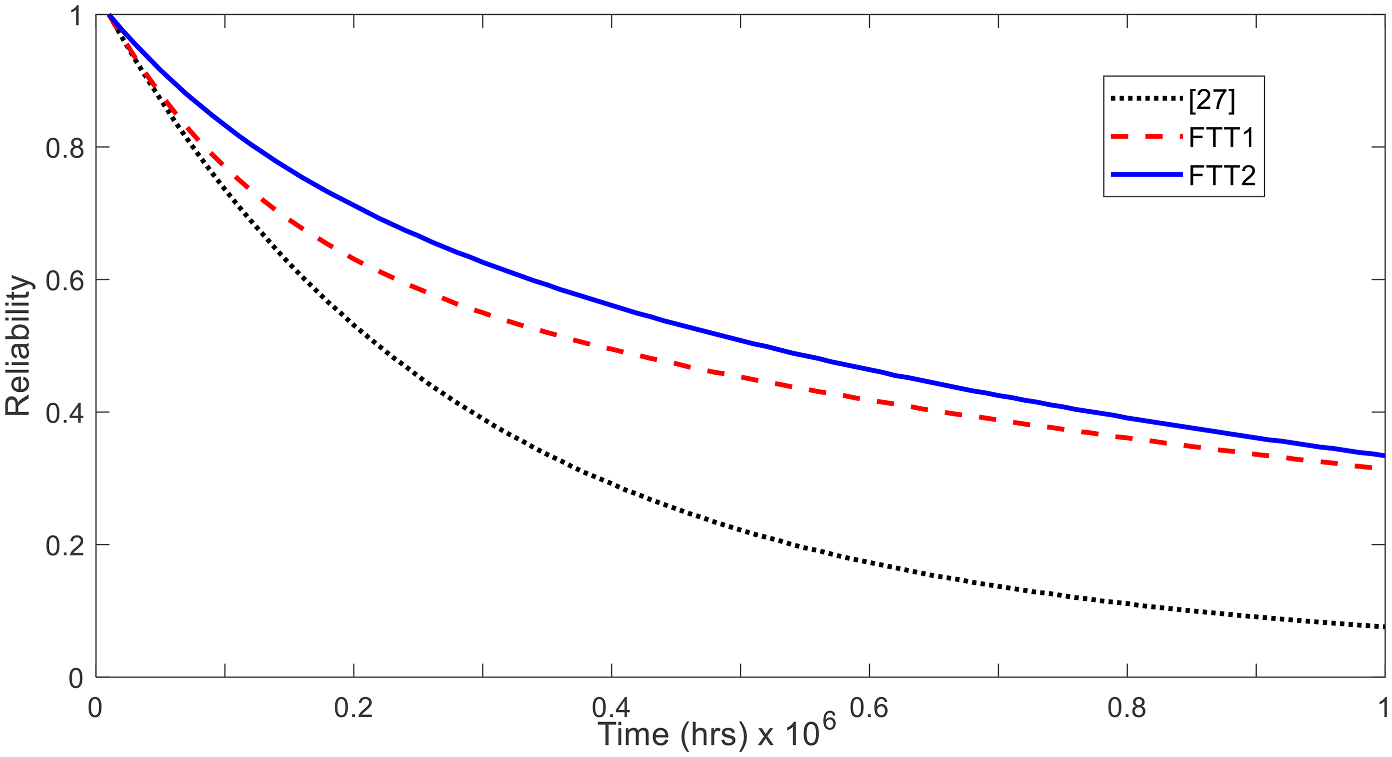
Reliability comparison among (Kim et al., 2019) and converters FTT1 and FTT2.
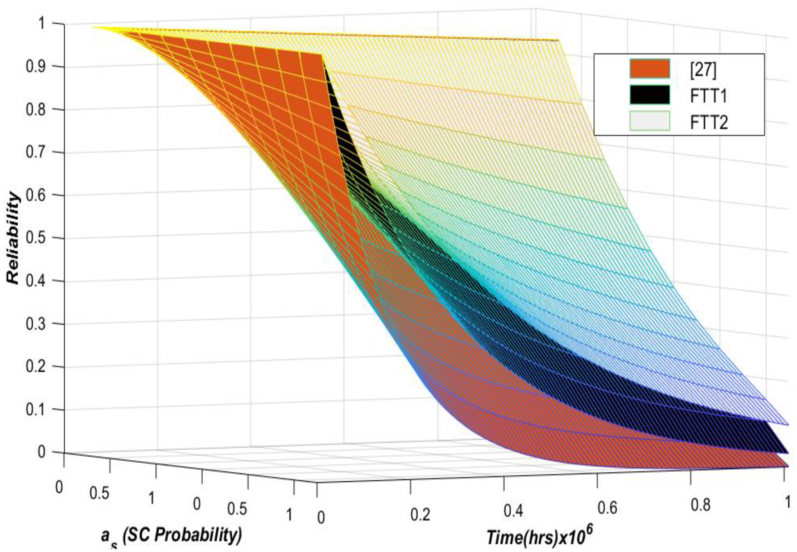
Reliability profile comparison with the change in as.
The failure rates of components are affected by various factors including electrolytic capacitors (μC), environmental conditions (μE), application specifics (μA), quality standards (μQ), voltage stress in capacitors and diodes (μv and μs), temperature variations (μT), and the base failure rate of each component
Transition probabilities between states are depicted in a matrix, with dimensions determined by the number of states considered. However, only the feasible states maintain nonzero values in the matrix. Let's denote the probability of a state as Qn(t), where “n” signifies the specific state for which the probability is defined. All probabilities can be expressed using the following relationship.

In a MRAA illustrating an FTT, where the states represent fault scenarios, it's apparent that reverting from one state to a previous one is not feasible. Therefore, the entries representing the reverse transition in the transition matrix can be substituted with nulls.
Furthermore, the diagonal elements 


Given that State-1 from Figure 13 represents a healthy state while the others signify faulty states, the preliminary status for the probability vector can be assumed as follows:
Utilizing the aforementioned equations, the reliability of the FTTs can be computed as
The reliability depiction of the FTT1 and FTT2 typically involves a study centered on the failure rates of its components, as indicated in Table 6. However, it is crucial to consider certain factors affecting the failure rates of different components, especially when dealing with sensitive converters. In the topology reported in Kim et al. (2019), operation is confined to one switch fault only, thus neglecting transition paths involving states 3 and 4. Additionally, the failure rate for the transition path from state 1 to 2 (i.e.
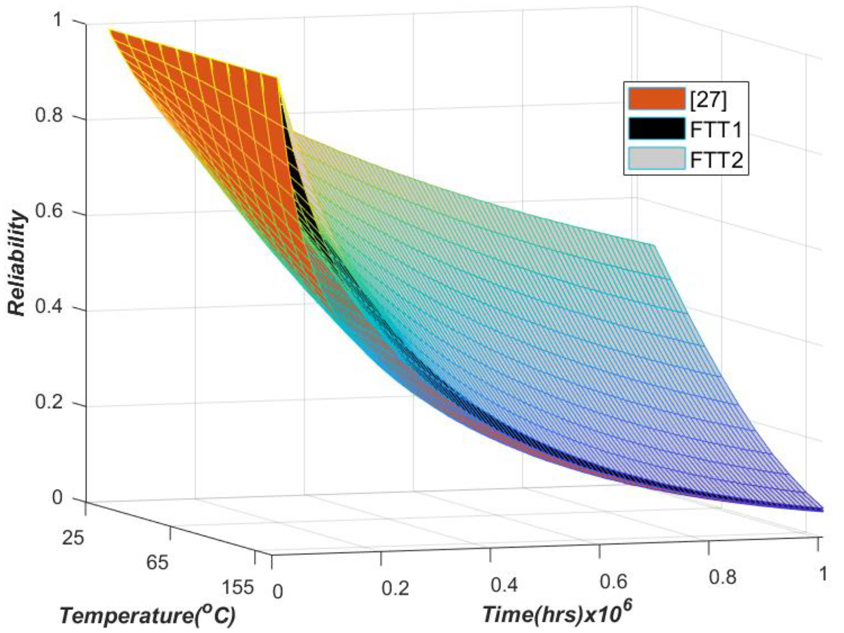
Reliability profile comparison with the change in Ta.
Component failure rate.
Reliability profile parameters.
FTT1: fault-tolerant topology-I; FTT2: fault-tolerant topology-II; MTTF: mean-time-to/between-failure.
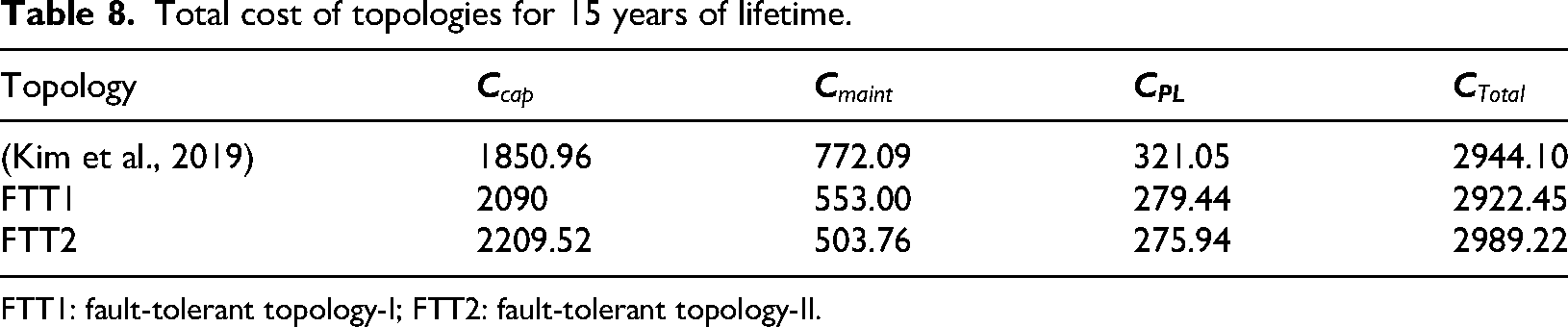
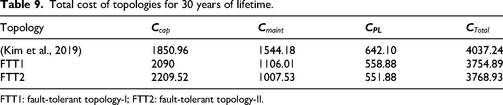
Cost analysis
This section deals with the investigation of the cost involved for both topologies, FTT1 and FTT2 based on their resiliencies. Any power converter's total cost includes capital, maintenance, and power loss costs. The capital cost is calculated based on the components used in the converter. For FTT1 and FTT2, the capital cost depends on the inductors, capacitors, semiconductor switches, and diode. As per Mouser (n.d.), the cost of components per item would be ₹208.33 for the inductor, ₹65.52 for the capacitor, ₹119.52 for the semiconductor switch, ₹10.22 for the diode. Hence, the capital cost for FTT1 and FTT2 can be obtained as:
Since the fault-tolerant strategy implemented is a reconfigurable type, the maintenance cost is expected to be minimal as it has no downtime period. Hence, the financial loss incurred during the operation can be neglected. However, for Y years of lifetime, the maintenance cost can be deduced based on the reliability of the converter as follows:
In addition, a power loss cost can be assumed to be around ₹0.5/kWh. Hence, a total power loss cost for a year can be calculated as
Using the equations (14)–(16), the total cost involved for the converter can be computed as:
Tables 8 and 9 show the total cost of the converters for a lifetime of 15 years and 30 years respectively. The tabulation in Table 8 deduces that the total cost of a converter with an expected lifetime of 15 years for Kim et al. (2019) is ₹2944.10, FTT1 is ₹2992.45, and FTT2 is ₹2989.22. Similarly, Table 9 shows that for an expected lifetime of 30 years, the total cost of converters in Kim et al. (2019) is ₹ 44,037.27, FTT1 is ₹3754.89, and FTT2 is ₹3768.93 (Components Costs). It is to be noted that all the converter costs are nearly the same and with the added advantage of being fully fault tolerant for FTT2, this can be an economic choice with better features of reliability, lesser power dissipation, regulated output voltage, single and multiple switch fault handling capability for both OC and SC type of faults.
Total cost of topologies for 15 years of lifetime.
FTT1: fault-tolerant topology-I; FTT2: fault-tolerant topology-II.
Total cost of topologies for 30 years of lifetime.
FTT1: fault-tolerant topology-I; FTT2: fault-tolerant topology-II.
Sensitivity analysis
The sensitivity of a power converter is defined as the relative change in the output voltage with respect to any change in the input voltage or any other parameters that affect the operation of the system, such as the duty ratio of the switches. In particular, the sensitivity of the system studied with respect to the duty cycle and input voltage defines the stability of the system. In general, the sensitivity of a variable p with respect to q can be written as
Hence, the sensitivity of system is evaluated for output voltage with respect to input voltage and the duty cycles of switches operated for various modes as discussed in previous sections. In this regard, the sensitivity of the system with respect to different parameters has been tabulated in Table 10.
Sensitivity analysis of reported topologies.
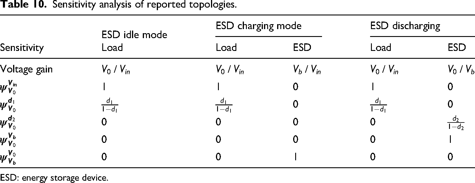
ESD: energy storage device.
Comparative analysis
In Table 11, some similar fault-tolerant topologies reported recently have been compared with FTT1 and FTT2. The advantages and limitations have been tabulated individually. As mentioned earlier, the modified boost converter in Kim et al. (2019) have fewer switches to operate. However, it is limited to single switch fault tolerant operation only, that is, on boost switch only. FTT1 has comparatively more switches. However, it can be operated as a fault-tolerant for all single switch faults and two cases of multiple switch faults. The second topology FTT2 has one additional switch compared to FTT1 to overcome the limitation discussed in the fault-tolerant topology-I section. Though this makes the topology completely fault-tolerant, the increased number of switches is still a limitation for this topology. However, the pros of FTT2 regarding the fault tolerance of single and multiple switches, the capability of handling OC/SC fault, regulated output voltage post-switch fault, and uninterrupted supply post-switch fault make it an apt choice for hybrid renewable energy-based applications.
Qualitative and quantitative analysis of fault-tolerant topologies.
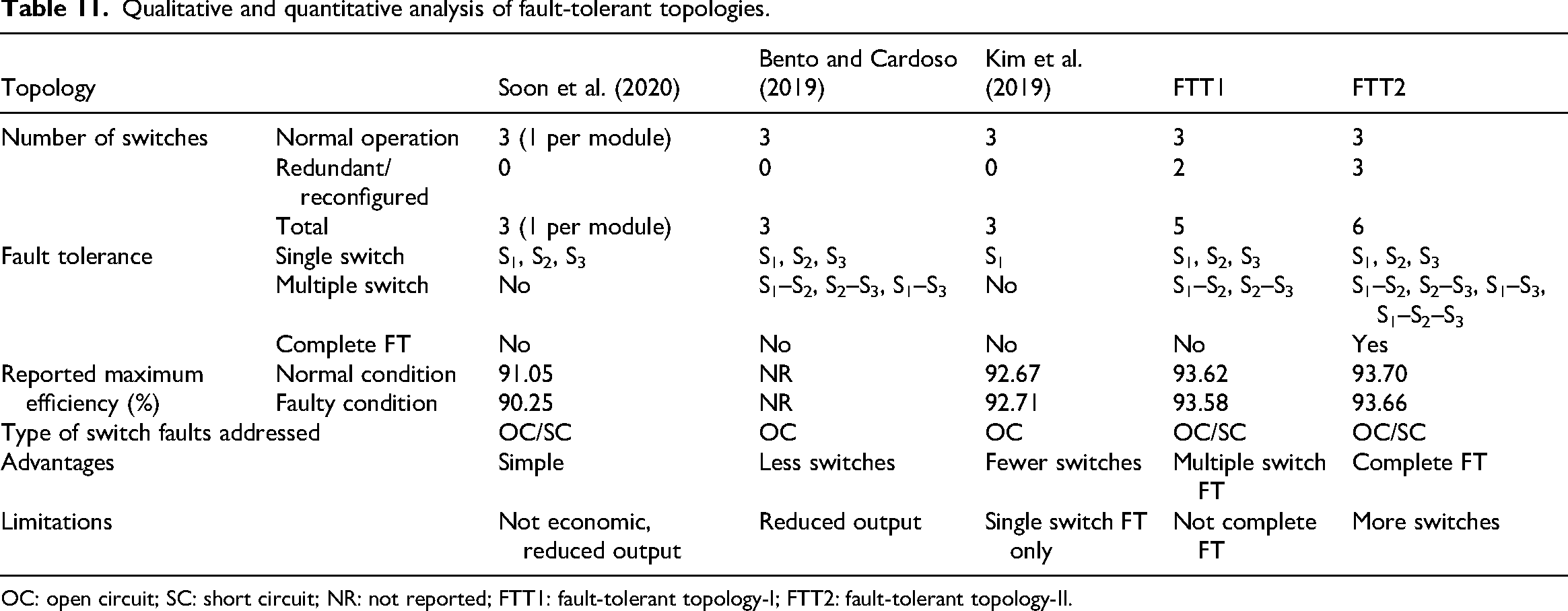
OC: open circuit; SC: short circuit; NR: not reported; FTT1: fault-tolerant topology-I; FTT2: fault-tolerant topology-II.
Conclusion
This article focuses on two reconfigurable multiport converter topologies with fault tolerance operation and their switching strategies, along with their performances for renewable-based hybrid standalone applications to provide an uninterrupted, regulated, efficient, and reliable supply for various probable combinations of switch fault scenarios. The laboratory prototypes for both the topologies, FTT1 and FTT2 have been developed, and the operation of converters with various fault scenarios has been studied and analyzed. The experimental results validate the performance of the reported topologies for a combination of various single and multiple switch fault scenarios. It has been observed that FTT1 is not completely fault-tolerant. Such limitation of FTT1 has been addressed in FTT2. It has been observed that FTT2 provides complete fault tolerance along with regulated output voltage, the capability to handle any type of switch faults, and the power demanded by the load. Further, the performance analysis with respect to losses, stress, reliability, and cost have been studied for both topologies. The empirical findings, performance analysis, and comparison with existing literature collectively suggest the superior effectiveness of FTT2 in renewable-based hybrid standalone applications.
Footnotes
Funding
The author(s) received no financial support for the research, authorship, and/or publication of this article.
Declaration of conflicting interests
The author(s) declared no potential conflicts of interest with respect to the research, authorship, and/or publication of this article.