
Abstract
Research in the physical sciences is critical to the development of new materials technologies for clean energy. Aims in the present work are to synthesise and characterise three-dimensional architectures composed of two-dimensional atomic layer molybdenum disulphide for solar cells and self-powered photodetectors with improved performance. Nanostructured molybdenum disulphide was prepared by using a spin coating method with controlled process times. Prior to each deposition, the layer was dried with hot air for 5 min. A rough, irregular and clustered surface type was generated when the number of spin coating runs was increased. This type of surface was consistent with the morphologies expected for two-dimensional atomic layer molybdenum disulphide in three-dimensional architectures. The nanoscale morphologies, composites, and electronic properties of molybdenum disulphide were examined using scanning electron microscopy, energy-dispersive X-ray spectroscopy, and micro-Raman scattering spectroscopy, respectively. Moreover, three-dimensional architecture-based prototypes for solar cells and self-powered photodetectors were designed, fabricated and tested. In photovoltaic mode, the obtained responsivity and response speed were almost 10 times larger and 20 times faster, respectively, than those recently reported for a single monolayer molybdenum disulphide-based self-powered prototype. In addition, the effects of bias, heat, humidity and a static field on the generated photocurrent and the response time were evaluated. It is expected that the newly designed prototype will exhibit exceptional properties: a broadband spectral response, a high signal-to-noise ratio and excellent stability.
Keywords
Introduction
Two-dimensional (2D) transition metal dichalcogenides have attracted considerable attention due to their excellent optical and electronic properties such as their tunable bandgaps and strong interaction. These materials exhibit immense potential for use in new generation solar cells (Jiao et al., 2015; Ruan et al., 2015; Sahito et al., 2016), photodetectors (PDs) (Liu et al., 2014; Tetsuka et al., 2016), gas sensors (Singh et al., 2017a, 2017b, 2019) and other optoelectronic devices (Aboutalebi et al., 2014; Chee et al., 2016; Kim et al., 2010, 2014; Krishnan et al., 2019; Li et al., 2012; Park et al., 2012). Various 2D nanostructures have been fabricated using (among others) mechanical and chemical exfoliation, chemical vapour deposition and atomic layer etching methods. Among these nanostructures, 2D molybdenum disulphide (MoS2) atomic layers are particularly interesting, owing to their high carrier mobility and optical transparency, which are highly desirable for solar cells and broadband PDs. Many good results have been reported (Gant et al., 2019; Li et al., 2020; Lopez-Sanchez et al., 2013; Tsai et al., 2014). For example, Tulsani et al. (2019) recently demonstrated the first-ever matrix-free deposition of 2D MoS2 sheets as an efficient hole transport layer for solar cells. In addition, Wang et al. (2015) developed an ultrasensitive and broadband MoS2 PD driven by ferroelectrics. The characteristics and applications of 2D MoS2 nanostructures have been systematically reviewed (Nalwa, 2020). Evidently, heterojunction multilayer nanostructures such as MoS2 with ZnO, TiO2 or BiFeO3 are essential components of solar cells or self-powered PDs.
In the present work, we extend our previous work on the use of wide bandgap boron nitride 2D sheets in deep UV PD by exploring, synthesis of emerging 2D atomic layer MoS2. Three-dimensional (3D) architectures composed of 2D atomic layer MoS2 with random orientation for high performance of solar cells and self-powered PDs were explored. This approach differed significantly from the approaches where heterojunction multilayer nanostructures were employed.
Syntheses
Several types of 2D MoS2 sheets were prepared in order to understand the evolution of surface morphologies and crystalline structures of 2D sheets and the effects of these morphologies and structures on prototypes. Nanostructured MoS2 was prepared by using a simple spin-coating method with commercial 2D MoS2 dispersion in solvents (dissolved in ethanol solution (density: 1 mg/mL) from XFNANO Materials Tech Co. Ltd). The thickness of the thin film deposited via this method is a function of the solution viscosity, density, rotation speed and time. Before preparing the sample, ultrasonic cavitation was used for 2 h to disperse nano-sized 2D sheets in solvents in order to break-up sheet agglomerates and increase the distribution uniformity. This contributed to a high specific surface area of each material.
We deposited films (thickness: ∼70 nm) at a spin rate of 1500–2000 min−1 for 20 s. However, the obtained MoS2 film appeared discontinuous and consisted of isolated segments and a few continuous sheets, with which no any types of solar cells and self-powered PDs could be made. Multiple coating for a continuous, thick film is unfeasible with the spin coating technique because each layer would be washed away by the subsequent layer. Therefore, prior to each deposition, the layer was dried with hot air for 5 min. This process was repeated several times until the desired film thickness was achieved. A rough, irregular and clustered surface type would become clearly visible following an increase in the number of spin-coating runs. This type of surface is consistent with the expected morphology of MoS2 films exhibiting a wide range of orientations. In contrast, every single sheet prepared in the first 20 s of the process appeared flat with a horizontal orientation.
Basic characterisation
The nanoscale morphologies and compositions of 2D MoS2 were examined by using JEOL 6480LV scanning electron microscopes (SEM) equipped with energy-dispersive X-ray spectroscopy (EDX) capabilities. Micro-Raman scattering spectroscopy was performed using a Jobin-Yvon T64000 Triple-mate system with the radiation of 514.5 nm from a coherent argon-ion laser, and a liquid N2 cooled charge-coupled device system was used to collect and process the scattered data. Electrical properties and light-generated photocurrent at different conditions (bias, wavelength, intensity and temperature) were assessed at the homemade test station (Feng and Aldalbahi, 2018). The measurements were performed under open-air atmospheric conditions.
Figure 1(a) shows a typical SEM image of nanostructured MoS2 prepared in the first 20s of the spin coating process. The sample consisted of a few isolated sheets and partially overlapped segments. Each continuous MoS2 sheet (average diameter: 1–2 µm2) was highly transparent. Figure 1(b) shows an SEM image of nanostructured MoS2 prepared in 10 runs (duration of each run: 20 s) of the process. The film consisted of numerous randomly orientated 2D sheets and was characterised by a rough surface. The surface area of the film was very highly exposed, owing to these irregular shapes. In the past, we have reported on boron nitride 2D sheets in 3D architectures for photovoltaic mode operations (Aldalbahi et al., 2017; Rivera et al., 2017). Based on that work, the expectation is that 3D architectures composed of 2D MoS2 atomic layers would be a desirable feature for solar cells and self-power PDs.
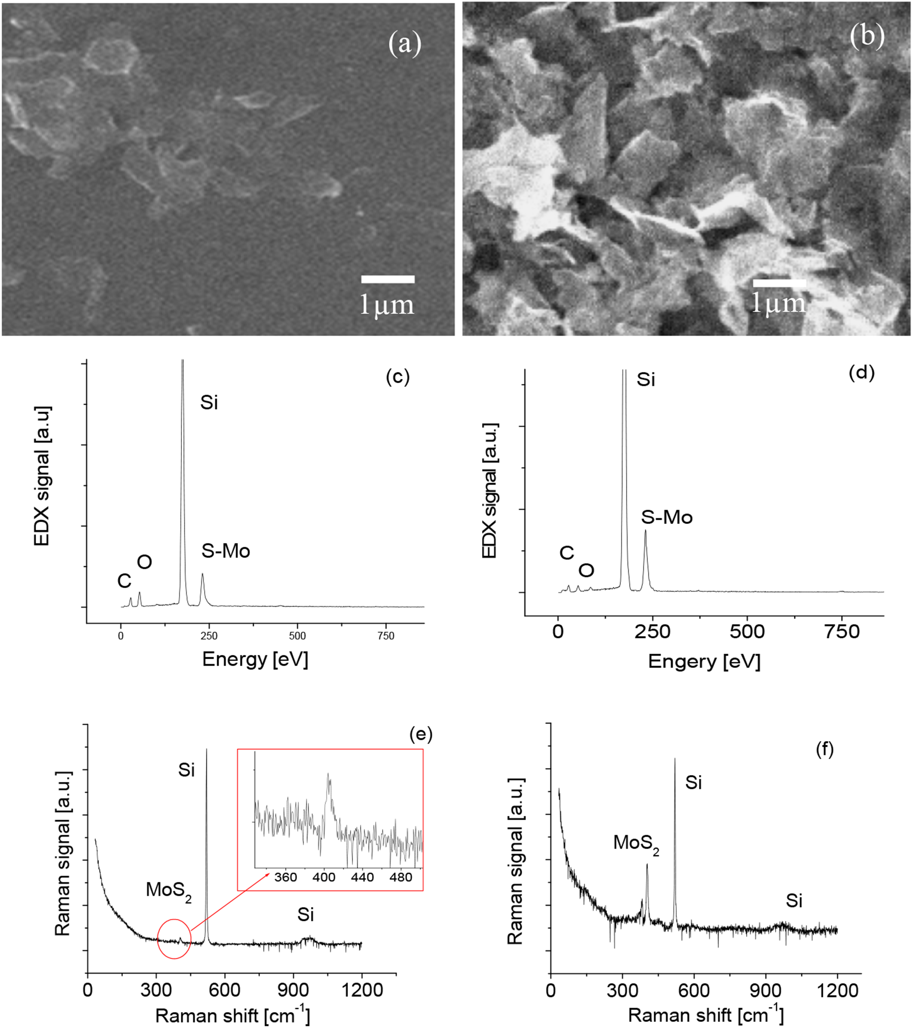
(a, b) Typical SEM images of nanostructured MoS2 prepared in one run and 10 runs, respectively, of the spin coating process, (c, d) EDX, and (e, f) Raman scattering spectra of two MoS2 samples (a, b).
Spin coating processes of fewer than five runs generated a MoS2 film with discontinuous structures, which, in most cases, indicate poor conductivity of the film. As shown in Figure 1(b), increasing the spin coating to 10 runs yielded numerous overlapped sheets that fully cover the surface area of the substrate. As a result, electrical properties such as the conductivity and carrier mobility of the sample can be significantly improved as confirmed by measurements of the electrical properties and light responses. The spin coating process can synthesise 2D MoS2 in 3D architectures with an extremely high specific surface area. This conventional process can replace other high technology methods due to its low synthesis cost and high light absorption efficiency. Therefore, our work on the development of broadband prototypes was based on the samples prepared through 10 runs of the spin coating process.
The compositions of the 2D MoS2 sheets are determined via EDX measurements of each sample. The typical EDX results of both samples are shown in Figure 1(c) and (d). Moreover, the EDX signal from the second sample is considerably stronger than that of the first sample, owing to their difference in thickness. The presence of S and Mo elements indicates the successful growth of the MoS2. Element ratios between the S/Mo atoms from MoS2 samples prepared for single run or 10 runs of spin coatings remained almost unchanged, slightly less than 2, suggesting there were little S vacancies in both samples that were associated with the n-type semiconductor behaviours. The substrate EDX signal was much stronger associated with the first sample than that of the second sample. This is because of their different thickness of MoS2 over layers.
Raman scattering spectroscopy with a 514 nm Ar+ laser as the excitation wavelength was also used to examine both samples. Raman active
Bias effect
Following basic characterisation, the prototype was fabricated and the light-generated photocurrent properties were studied. The process flow of the MoS2 prototype fabrication is similar to boron nitride PD (Aldalbahi et al., 2017; Rivera et al., 2017). Briefly, plasma sputtering was used to deposit ∼100 nm thick Pt and Al electrodes at the two ends of the sensing layer, respectively. The space between the two electrodes is 3 mm and the width of the same is 3 mm so the total exposed area is 9 mm2. Then, the sample was connected to an electric circuit to form a prototype. A planar structure of electrodes was employed in order to optimise the photo-electron collection near the surface. The sensing layer consists of a large amount of MoS2, and the thickness of the layer was around 1–2 µm. No precise measurements could be carried out because 2D sheets were heavily overlapped each other with random distributions, resulting in a highly rough surface.
All measurements were conducted under standard ambient conditions. Figure 2(a) shows the typical light-induced or light-generated photocurrent as a function of time when the prototype was exposed to a square-pulse 750 nm light illumination at different applied biases. Figure 2(b) shows the typical photocurrent as a function of applied bias at an illumination intensity of 0.16 mW/cm2. The differences between the light-induced photocurrent during turning on or off light illumination were easily identified. The response strength or photocurrent increased with an increase of bias.
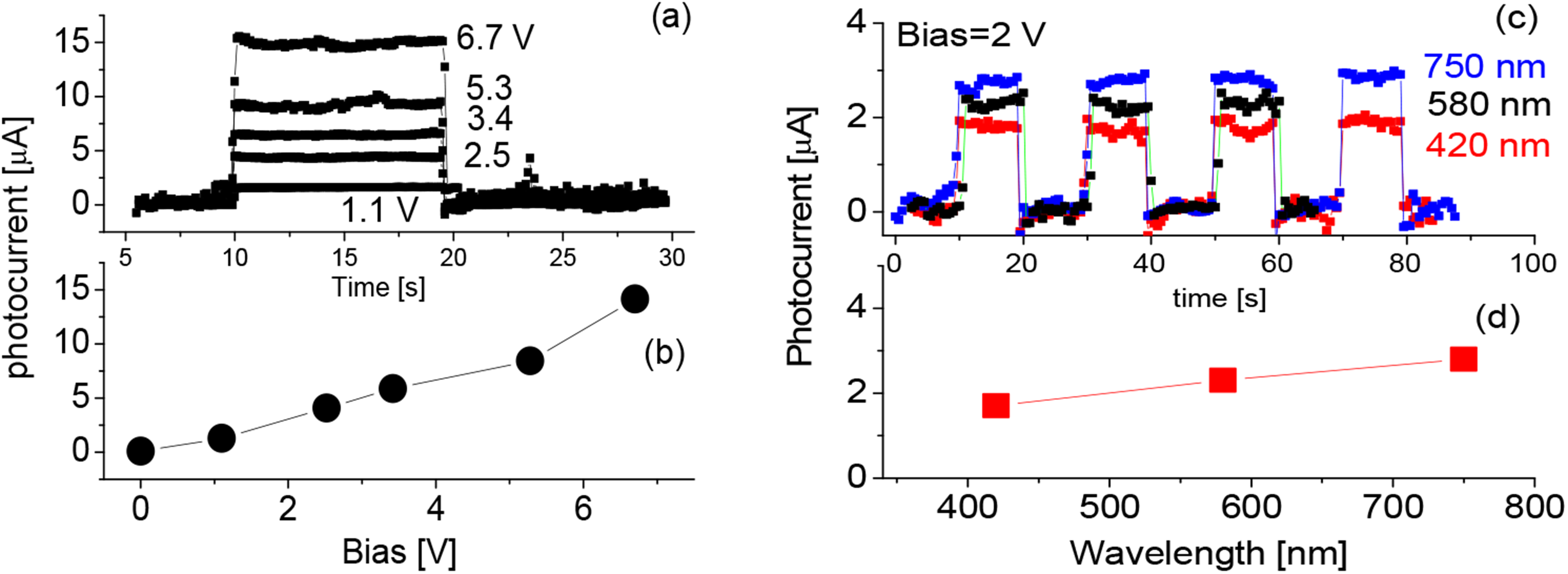
(a) 750 nm light-induced photocurrent as a function of time at different bias, (b) photocurrent as a function of bias at 0.16 mW/cm2 light illumination and (c) effect of bias on the photocurrents generated with different wavelength light illuminations. (d) Photocurrent strength vs wavelength of light illuminations at the same power density.
Spectral response to photo illuminations
Further experiments were also conducted for measuring the spectral response. Figure 2(c) shows the typical results obtained during cyclic tests. Good repeatability and stable baseline features were easily observed. When the prototype was exposed to 750 nm light illumination, the light-induced photocurrent (Iph) increased rapidly in the initial period, and then reached a maximum of ∼2.7 µA. Once the light illumination was turned off, the photocurrent dropped quickly. The mechanisms leading to light-generated photocurrents are discussed elsewhere (Gant et al., 2019; Li et al., 2020; Liu et al., 2018). The yielded photocurrent was directly associated with MoS2 light absorption. Furthermore, the exposed area (Aarea) of the active layer was ∼9 mm2 and the 750 nm illumination power density (Iintensity) was 0.16 mW/cm2, resulting in an illumination power of Pλ = Iintensity × Aarea on the active layer surface (λ: excitation wavelength). Accordingly, a responsivity Rλ (defined as the ratio of the generated photocurrent Iph and the illumination power Pλ) of ∼0.2 A/W was obtained. The photocurrent or responsivity was increased by increasing the applied bias. However, the present work focused on photovoltaic mode operation. The obtained value is comparable to values recently reported for monolayer MoS2-based devices (Gant et al., 2019; Li et al., 2020). In our case, the prototype is characterised by a clearly defined response signal and a better signal-to-noise ratio than those of previously reported devices.
The fabricated prototype exhibited a slightly higher response strength to the longer wavelengths of light illumination than that to shorter wavelengths. For example, 0.16 mW/cm2 580 nm illumination yielded a maximum induced photocurrent of 2.2 µA, and 420 nm illumination generated a photocurrent of ∼1.95 µA. The MoS2-based prototype exhibited a very broadband spectral response ranging from violet (420 nm) light to near-infrared light (750 nm) as shown in Figure 2(d). However, estimation of a cutoff wavelength was prevented by the lack of a light source with a longer wavelength than the wavelength range observed.
Broadband phenomena with 2D MoS2 active layers have been reported in a previous study (Nalwa, 2020). The increase in the interlayer spacing of the 2D MoS2 sheet may have contributed to the magnitude of the observed broadband structures. Some impurities may have also contributed mid bandgaps. If impurities were responsible for the apparent bandgap change, the expectation is that the generated photocurrent and the signal-to-noise ratios would decrease considerably with increasing temperature. These phenomena were manifested as a poor signal-to-noise ratio and a decrease in the photoresponse with increasing operating temperature (as discussed in the subsequent section).
Photovoltaic mode operation
In order to explore potential applications such as solar cells and self-powered PDs, experiments similar to those described in the previous section (see Figure 2) were performed but the external power supply was removed. The prototype was cycled with an on–off period of 2 min under 750 nm light illumination (see Figure 3(a)). When no external power supply was employed, the MoS2-based prototype still exhibited a clean response with a well-defined and stable baseline, demonstrating that the prototype is capable of photovoltaic mode operation. In fact, the prototype was retested after four weeks and all the experimental values remained nearly the same, except for a humidity effect as discussed in a subsequent section.
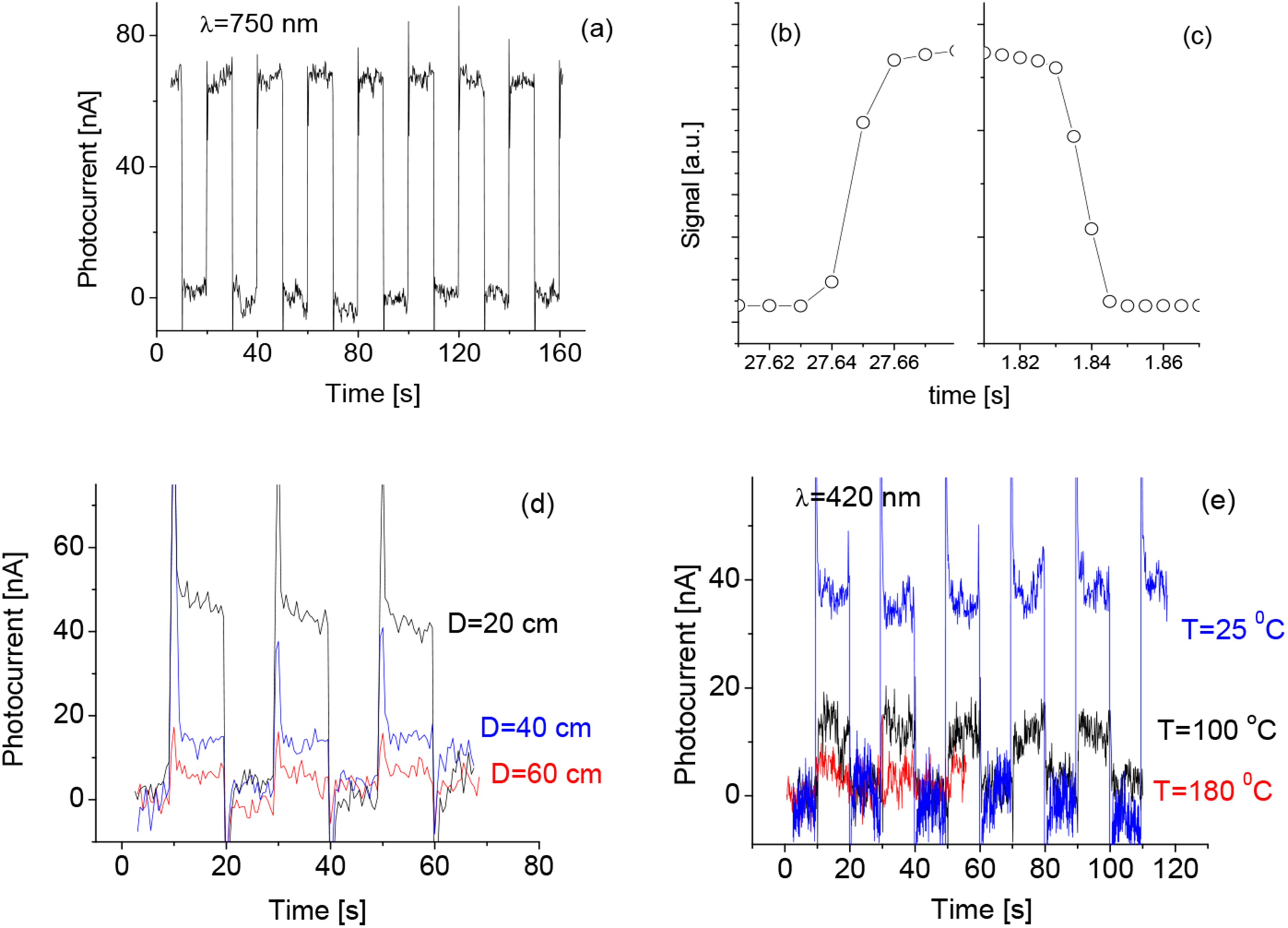
(a) The time response of the molybdenum disulphide (MoS2)-based prototypic solar cell exposed to 750 nm light illumination at an intensity of 0.16 mW/cm2, and (b, c) rise and recovery times. Effect of (d) illumination power density, and (e) operating temperature on light-generated photocurrents.
The experimental data shown in Figure 3(a) indicated that light illumination with a power density of 0.16 mW/cm2 generated a maximum photocurrent of Iph = 68 nA. The exposed area of the active layer was ∼9 mm2, and hence a responsivity Rλ = Iph/Pλ of 4.96 mA/W was obtained. This value is almost 10 times larger than that recently reported for a single monolayer MoS2 based self-powered prototype (Liu et al., 2018). An additional advantage in the present case was that the fabrication process was extremely simple, and could be performed without a microelectromechanical system (Liu et al., 2018).
In the present case, the photovoltaic mode operation with improved performance could be performed without an external energy source and appeared to have a good signal-to-noise ratio and high stability. This resulted most likely from the extremely low dark current or weak noise background.
Time response
The rise time and recovery time of the prototype exposed to light illumination were also measured (see Figure 3(b) and (c)). The rise time was slightly longer than the recovery time but both were less than 15 ms. Furthermore, a high responsivity and a short response time were achieved. In other words, the response speed of the obtained 2D MoS2 in the 3D-architecture-based prototype is more than 20 times faster than that of a single flat MoS2 monolayer (Gant et al., 2019; Li et al., 2020; Liu et al., 2018).
The theoretical limit of the response speed depends on the transit time of electrons and holes in the device, the carrier diffusion and the carrier multiplication process in the MoS2, as well as the circuit time constant. The response speed of the present prototype should be faster than the value realised. That is, owing to the high carrier velocity of MoS2 and the improvement in the crystallinity of 2D MoS2, the recombination would be quickly reduced and the response time would be shortened. The real rise and recovery times should be shorter than the obtained values. A slightly longer response time may have resulted from a time delay in reaching the full intensity after the LED lamp is turned on, and residual photo-luminescence after the LED light is turned off.
Effect of light intensity
To understand the effect of light intensity, the distance between the LED light source and the prototype was varied in order to control the power density of light illumination on the surface of the active layer. The light illumination intensity on the active layer decreased following an increase in the distance (D) between the prototype and the light source. Since the light source is a point type of LED, a spherical model was employed to estimate the intensity of the light illumination on the surface of the layer. A light intensity of ∼0.16 mW/cm2 was obtained for the prototype located at a distance of D = 20 cm away from the LED. Correspondingly, the 580 nm light-generated photocurrent and the responsivity were 53 nA (as shown in Figure 3(d)) and 3.9 mA/W, respectively. Similarly, when D = 40 and 60 cm, illumination densities on the surface of the active layer were 0.04 and 0.017 mW/cm2, and the generated photocurrents were 13 and 6 nA, respectively. The obtained responsivities remained nearly unchanged, at ∼3.9 mA/W, for all cases with 580 nm light illuminations.
Effective operating temperature
For most of the effective operating temperatures reported for various semiconductor-based electronics, a maximum operating temperature before thermal noise completely saturates the signal of the detectors has been consistently encountered. Comparisons of the 420 nm light-generated photocurrents obtained at room temperature, and at 100°C (see Figure 3(e)) revealed that a high operating temperature would result in an intense noise signal and relatively low photocurrent. That is, the obtained photocurrent dropped from 40 to 15 nA and then to 9 nA when the operating temperature increased from room temperature to 100, and then to 180°C. Increasing the operating temperature led to a significant decrease (by a factor of ∼2 and 5) in the light-generated photocurrent and signal-to-noise ratio compared with the ratio corresponding to room temperature.
The decrease in the photocurrent with increasing operating temperature has been reported in previous studies (Aldalbahi et al., 2016; Rivera et al., 2018). This effect was generally attributed to an increase in impurity scattering following an increase in the operating temperature. However, identifying the dominant factor is challenging.
Humidity effect or static electric field effect
The humidity effect or the static electric field effect on the light-generated photocurrent was also observed. The response strength of each cycle varied in the first several cycles although the power intensity of illumination was the same. The induced photocurrent increased with the passing of each cycle, and then reached a stable state after ∼20 cycles, as shown in Figure 4(a). This resulted from the environmental humidity, which is one of the main factors that influence the performance of the prototype. Water molecules adsorbed on the surface would contribute no electrons to the MoS2 active layer but would partially absorb light, thereby affecting the response signal or photocurrent. The reaction between the active layer and the water molecules might lead to the gradual formation of stable chemical bonds on the active layer surface (Aldalbahi et al., 2016; Velazquez et al., 2016). Exposing this layer to light illumination would cause partial vaporisation of water molecules from the surface. The humidity effect on the properties of the prototype is highly dependent on the competitive surface effects resulting from absorption/desorption and the related ionisation/dissociation of water molecules on the photo-generated charge carriers. In contrast, a static electric field effect is one of the factors that induce a shift in the photocurrent, as shown in Figure 4(b). Based on semiclassical wave packet dynamics, these shifts may have resulted from dubbed jerk, injection and shift currents, and the photocurrents were probably induced by the injection and shift currents of the bulk photovoltaic effect (Fregoso, 2019). Recent research has indicated that the generated photocurrents could also be spin-polarised. The application of a relatively small static field can affect the spin-polarisation for some photon energies (Bezerra et al., 2014). Further investigation of these effects is required.
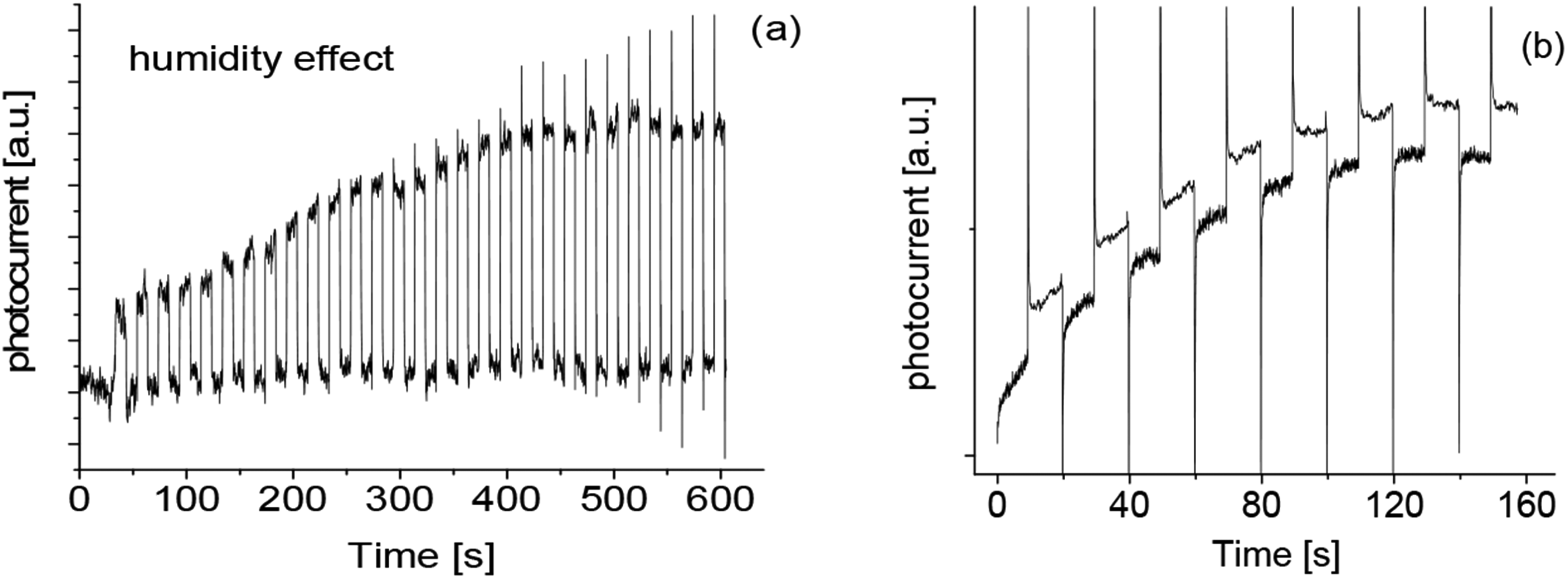
Effects of (a) humidity and (b) static electric field on light-generated photocurrent.
Conclusions
The syntheses involved a simple and cost-effective spin coating method for preparing 3D architectures composed of 2D atomic layer MoS2 without the use of complex heterojunctions and multilayer nanostructures. However, this method yielded excellent performance for solar cells and self-powered PD applications. We demonstrated, via experiments, that the fabricated prototype has a fast response time, high responsivity, good stable baseline and excellent repeatability, as well as a very broadband spectral response ranging from violet (420 nm) light to infrared (λ = 750 nm). The results indicated that the prototype with the 3D architecture composed of 2D atomic layer MoS2 is capable of photovoltaic mode operation. More importantly, the fabrication process can be performed without a complex microelectromechanical fabrication system. The main limitation is its efficiency is still not high enough as compared to Si-based solar cells. Future work would be focused on hetero nanostructures or multi-junction 2D atomic layers in order to achieve a higher conversion efficiency of a photovoltaic cell.
Footnotes
Acknowledgements
This project was funded by the National Plan for Science, Technology and Innovation (MAARIFAH), King Abdulaziz City for Science and Technology, Kingdom of Saudi Arabia, Award no. 14-ENE1986-02.
Author contributions
All authors worked together on designing and performing the experiments, as well as analysing the data and writing the manuscript.
Declaration of conflicting interests
The authors declared no potential conflicts of interest with respect to the research, authorship and/or publication of this article.
Funding
The authors disclosed receipt of the following financial support for the research, authorship, and/or publication of this article: This work was supported by the King Abdulaziz City for Science and Technology (grant no. 14-ENE1986-02).