
Abstract
The electronic system of the multi-chip combined control architecture satellites often requires an on-orbit reconfiguration capability for field programmable gate arrays (FPGAs). The purpose is to provide program backup and rapid on-orbit reconfiguration of the FPGA once suffering single particle event. Spacecrafts in low Earth orbit (LEO) are subject to the South Atlantic Anomaly (SAA), while deep space spacecrafts operate in an environment constrained by high levels of particles and radiation, intermittent communications, and limited resources, which together pose a significant challenge to the reliable operation of spacecraft electronics. Multi-chip flash process control is an effective solution to this challenge. In this work, we propose and implement a design for the GTM payload onboard the deep space DRO-A satellite, using an MCU, an FPGA, and flash memory, where the MCU is used to communicate with external data, write the FPGA bitstream frames to the flash, and serves as the control core for the data interaction between the off-chip flash memory and the FPGA via SPI. This configuration ensures the independence of the data interaction since the FPGA is not physically connected to the flash. The software uses a three-mode redundancy system, file CRC checksums, and data sending/receiving checksums to increase reliability. Prior to the launch of the DRO-A satellite, the program was comprehensively tested on the GTM payload. This design is important for extending the spacecraft and payload operational life under extremely harsh conditions.
Introduction
FPGAs are widely used in electronics design and applications in aerospace because of their high-speed computing capabilities and rich peripherals. Studies have shown that, as the ambient protons or neutrons flux increases, SRAM-type FPGAs not only exhibit single-bit flip but also greatly have a higher probability that adjacent bits flip simultaneously.1–3 However, flash-based FPGAs have stronger anti-flip capabilities, and embedded flash chips can still maintain an initial bit error rate below
For spacecrafts in Low Earth Orbit (LEO), it is almost inevitable for them to cross the SAA radiation region and suffer from high particle flux. Therefore, some chip reconfiguration schemes are proposed for program recovery in extreme situations.7–12 Common in-orbit reconfiguration methods include Joint Test Action Group (JTAG), SPI Slave, Analog JTAG, and Passive Serial Interface. The FPGA in-orbit reconfiguration function has been validated on some space programs, such as QPS-SAR-2 13 and the XL payload of the GOMX-5 14 satellites.
GTM is an astrophysical payload on the DRO-A satellite and is connected to the spacecraft electronics through the Payload Management Unit (PMU).15,16 The DRO-A satellite will be launched to the Distant Retrograde Orbit (DRO) orbit, which is about 300,000–400,000 km from the Earth. It will pass through the Earth’s radiation belt several times during the launch and dock in deep space orbit with the power on. Compared to other GECAM satellites7,17 in the low to medium-height Earth orbit, GTM will experience instantaneous particle impacts that are more than 100 times stronger (see Figure 12 in Appendix).
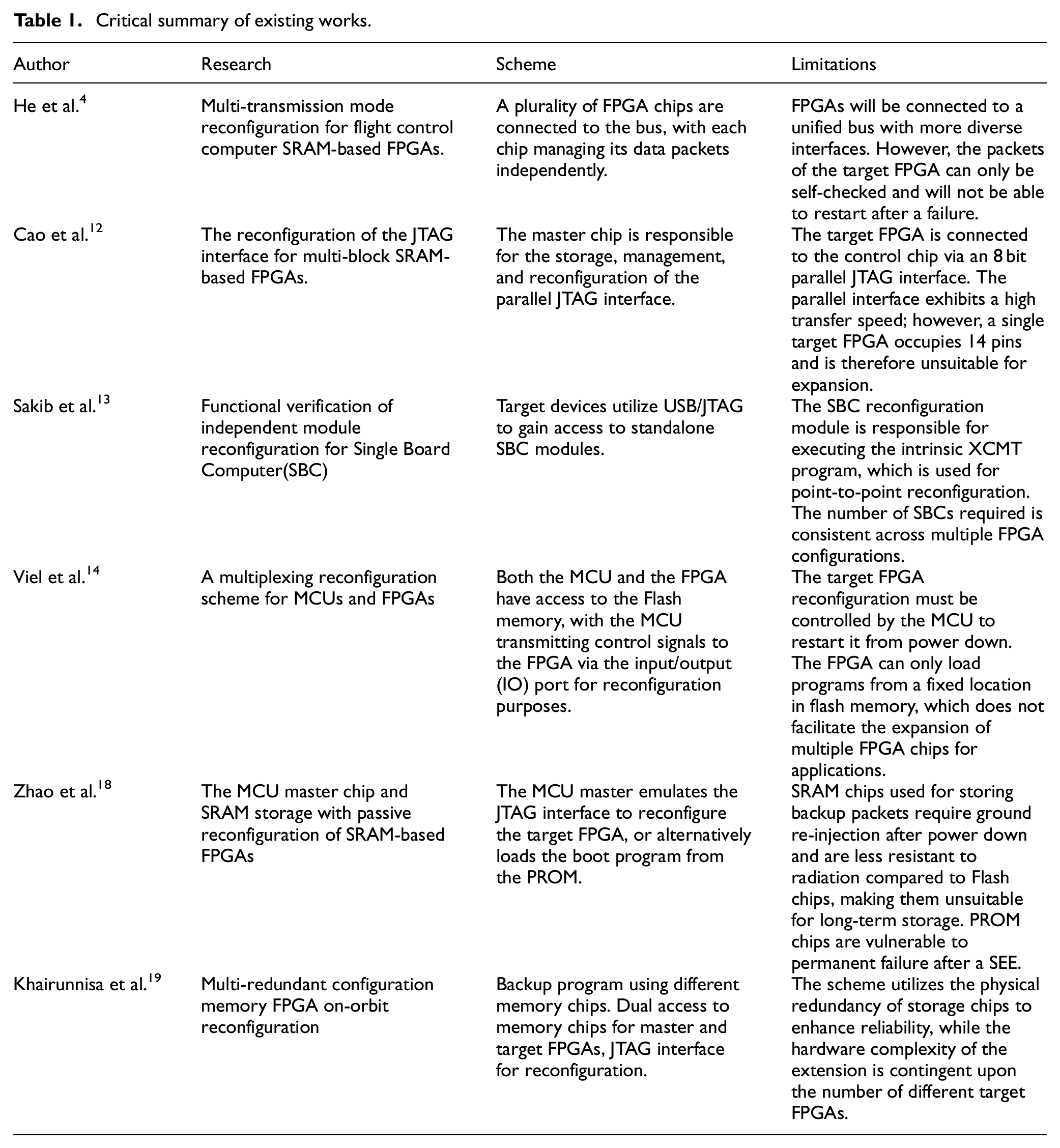
The most widely used solution in the aerospace field is a dual-core control architecture to achieve fault detection and active reconstruction of target FPGAs. For LEO equipment, there is usually sufficient power or greater communication bandwidth from the ground to the satellite, so RAM-type FPGAs are often used in combination with PROM dynamic refresh chips or flash memory chips to achieve reconstruction capability. However, the GTM payload equipment operating in the DRO deep space orbit does not have the conditions for high bandwidth and frequent maintenance, and the requirements for data reliability are more stringent. Using a simulated JTAG interface for a single FPGA chip is a good choice, but it will occupy too many IO pins when applied to multiple target FPGA chips. Therefore, we propose to design the flash chip memory scheme with MCU as the master. A single memory chip stores multiple versions of redundant programs from multiple target FPGAs to reduce memory chip redundancy. The use of SPI interface reduces the pin occupancy caused by expanding multiple FPGA chips when using JTAG interface, and focuses on the reliability of packet storage and reconstruction process. A critical analysis of the existing works has been presented so as to highlight the contribution of the proposed research work with respect to the already existing works, as shown in Table 1.
Critical summary of existing works.
Hardware design
To ensure long-term stable operation for GTM, we not only select devices with strong anti-interference ability in the space environment, but also design the on-orbit reconstruction function. There are the following requirements for the abnormal reconstruction function:
Implement proactive refactoring to ensure exception detection and recovery, as well as normal program updates and maintenance.
Equipped with multiple FPGA chips with different functions to achieve individual reconstruction of each FPGA chip.
Focuses on the accuracy of long-term data storage and reduces the power consumption caused by frequent refreshing.
Ensure data accuracy as much as possible, with a reconstruction time limit of 20 min. If the time exceeds 30 min, the GTM detector may be affected due to the failure of the FPGA thermal control function.
For the GTM payload, we select the Microchip’s M2S090 FPGA chip, which is a Flash-type chip that is not susceptible to particle overturning.6,10,20 The main control MCU is a Cortex-M7 core SAMV71 chip, 21 which has been verified for reliability in the GECAM mission. The SPI Flash chip S25FL512S, with a capacity of 64M bytes, is used to store the FPGA image program package. The schematic diagram of each structure is shown in Figure 1.
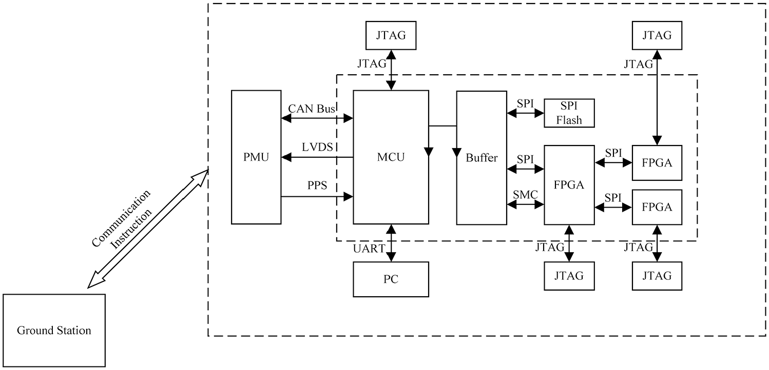
Schematic diagram of the FPGA reconstructing method proposed for the GTM payload onboard the DRO-A satellite.
Due to the considerable number of payloads carried by the satellite, differential signals are employed for data transmission over the CAN bus. This is done to circumvent the potential for single-ended common-mode interference that could arise from the operation of other payloads. The MCU receives ground commands and program packet data from the PMU over the CAN bus. Subsequently, the bitstream image files of the MCU and FPGA are stored in a flash memory chip. During global static reconfiguration of the FPGA, the MCU and FPGA interact via SPI to circumvent local dynamic configuration. 21
The SPI interface occupies only four IO pins, and the significant advantage of using the SPI interface over the JTAG interface, which occupies 10 I/O pins, is that the number of chips used on-board is greatly reduced.19,20 To facilitate ground testing, the MCU prints debugging information through the Universal Asynchronous Receiver/Transmitter (UART) serial port, while the FPGA and MCU are tested through the JTAG interface. The hardware circuit diagram is shown in Figure 2.
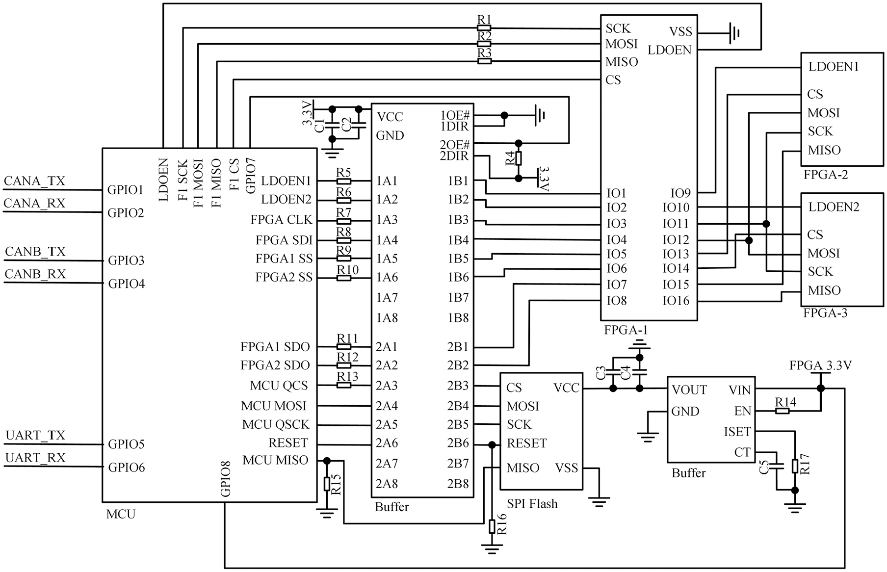
Hardware circuit of FPGA reprograming designed for the GTM payload.
Each FPGA and flash memory chip is isolated from the others, and the current consumption of each chip is monitored by the MCU. A software exception is defined as occurring when the current consumption of the FPGA reaches a predefined alarm value over a specific continuous period. At this juncture, the FPGA power will be disconnected and the status will be transmitted to the ground, which will then select the subsequent operation.
Software design
Bitstream image ground processing
The Bitstream mirror packet size is 4M bytes, constrained by the ground-satellite data transmission bandwidth. To facilitate processing, it must be divided into shorter frames on the ground. Concurrently, to facilitate the writing of data frames in an arbitrary order, as well as in the event of packet loss, error code, or code loss, the objective is to compensate for the loss of frames by making up for it. This is done to avoid the bandwidth consumption that would result from the re-uploading of all the data frames of the data packet. Furthermore, apart from increasing the fixed frame header and footer, as well as the frame data checksum and other conventional parameters, additional parameters such as the frame number, data destination address, and so on, are set within the data frame. In the event of the detection of a data frame error, it is sufficient to retransmit the data frame in question.
The original mirror file is aligned by 512 bytes and split into six short data frames, each with a variable length of valid data within the frame. Upon receipt of the message frame by the MCU, the complete packet is written to the off-chip flash memory. The bitstream mirror packet ground processing flow, along with the data block type and offset address within the packet, is depicted in Figure 3.
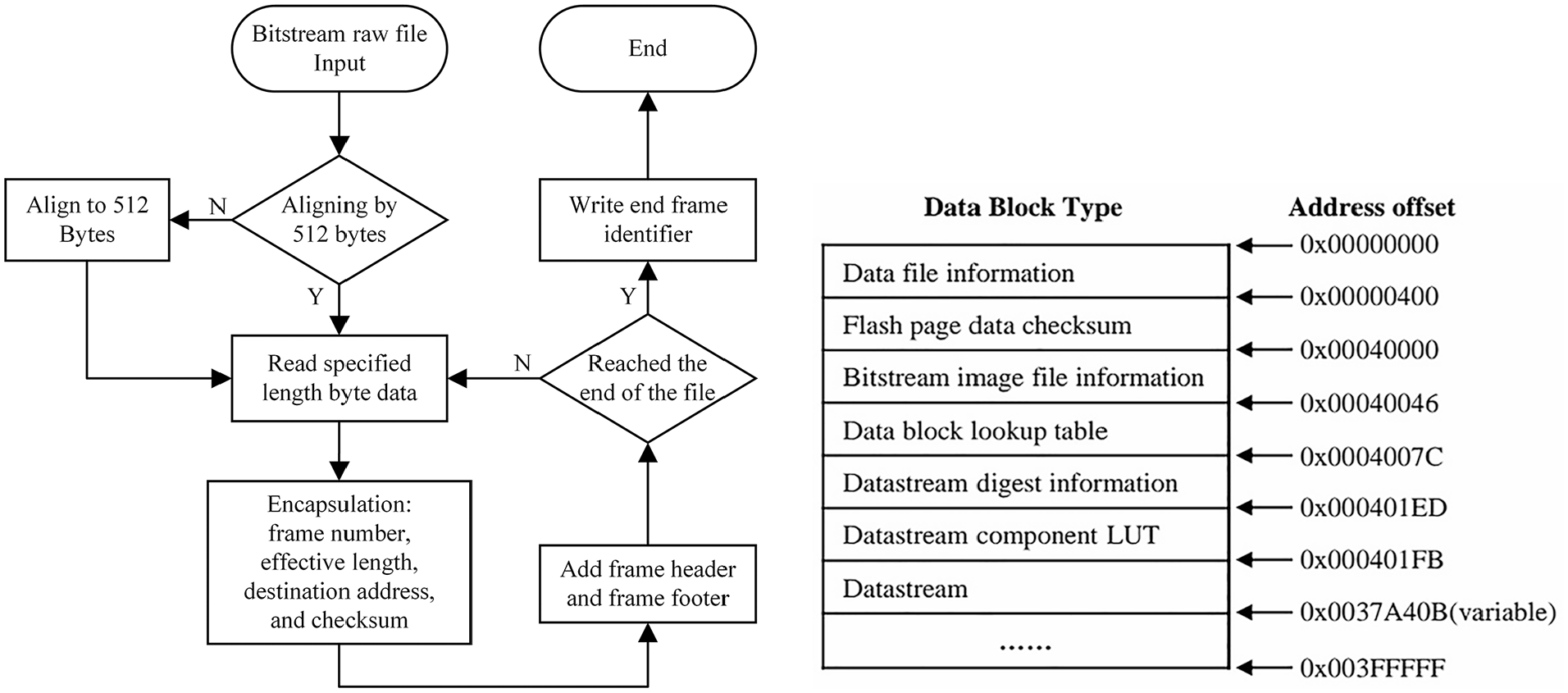
The left diagram depicts the flowchart of ground processing FPGA bitstream files, while the right figure illustrates the structure in flash subsequent to the completion of the data upload.
Data packet transmission design
The data packets can be uploaded to the satellite receiving equipment according to the available transmission mode, and then forwarded to the GTM through the PMU, which sends and receives commands and data through the CAN bus. The primary and backup copies use the received data alternately to enhance the anti-jamming capability of the link layer.
The instruction frame data volume is relatively modest, yet it necessitates a swift response. However, the data frame is unable to accommodate the demand, as the data volume is considerable. Consequently, the CAN bus message will be divided into two distinct frames: a single frame instruction frame comprising eight bytes and a composite message frame spanning from 9 to 512 bytes. Once the single-frame command message has been transmitted, there is no need for data splicing, as it can respond promptly to FPGA on-orbit reconfiguration parameter setting and execution. Composite message frames are used to perform operations on complex data, such as bitstream program data, satellite periodic broadcast data, and other data types. The bitstream image packet file, following ground data processing, constitutes a composite message frame. The GTM receives the PMU polling request and responds with an answer packet containing the current reconfiguration status, execution progress and other pertinent information.
Upon receipt of a CAN message frame, the MCU initially identifies the message frame type. If the frame is a single frame command, it is executed immediately following the verification of the checksum. If the frame is a long composite message, the header and footer identifier, CRC checksum value, node ID, and message type are verified. If the frame is a broadcast data frame, only the data is extracted. If the frame is a polling message frame, an answer packet is sent to the PMU. Finally, if the frame is a data frame, the data is written into Flash after verification. Upon the reception of a new frame, the frame reception count within the answer frame is incremented by one (initial value 0x00, reset upon overflow). Similarly, in the event of an erroneous data frame, the error instruction count within the answer frame is increased by one (initial value 0x00, reset upon overflow). Upon reception of the final frame of the mirror file data packet, the mirror data packet, spliced into flash memory, performs a file verification and writes the verification result into the answer packet. The CAN bus communication flow chart is illustrated in Figure 4.
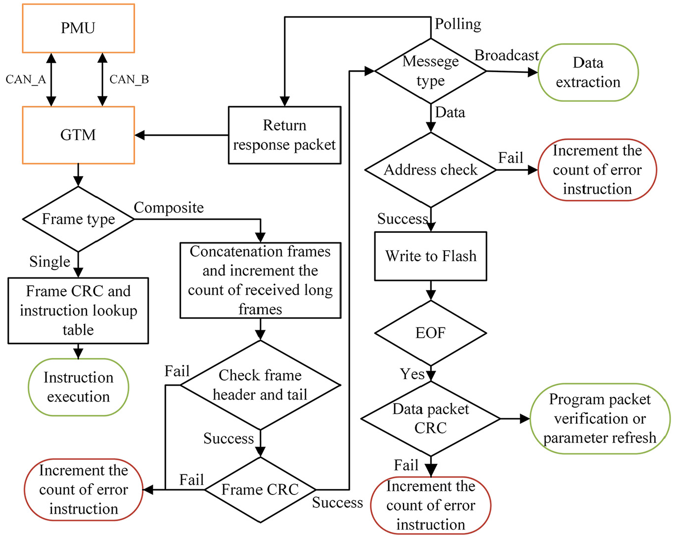
CAN message processing flowchart.
In-orbit reprograming design
Data interaction interface
In addition to in-orbit update requirements, GTM also should meet the requirement of real-time trigger information downlink and data processing onboard the satellite, therefore, running the uCOS III operating system on the MCU, the FPGA in-orbit reconfiguration function is classified as a high-priority independent task, which is accessed when the FPGA in-orbit reconfiguration instructions forwarded by the PMU are received and the reconfiguration process is performed. The SPI interface utilizes four IO lines, namely clock (CLK), master input/slave output (MISO), master output/slave input (MOSI), and chip select (CS). These lines are employed by the MCU to access the flash memory or FPGA. The CS line is set low by the MCU when accessing the flash memory or FPGA chip, and it is set high when the access is finished. To prevent contamination during data interaction, the off-chip flash memory and the first-stage FPGA chip do not share the SPI bus. Consequently, the MCU accesses the flash memory and the FPGA chip independently. To improve the data accuracy during the transfer process, a small amount of data is transferred in a single data interaction, and the data is written several times. The data interface between MCU and FPGA is set as single-byte command data Cmd, 16 byte send buffer Input_buffer, 16 byte receive buffer Output_buffer, single data interaction frame consists of command bytes and buffer data totaling 17 bytes, MCU sends the data using the Input_buffer, and the MCU receives the data using the Output_buffer. The flowchart of single data interaction between MCU and FPGA is shown in Figure 5.
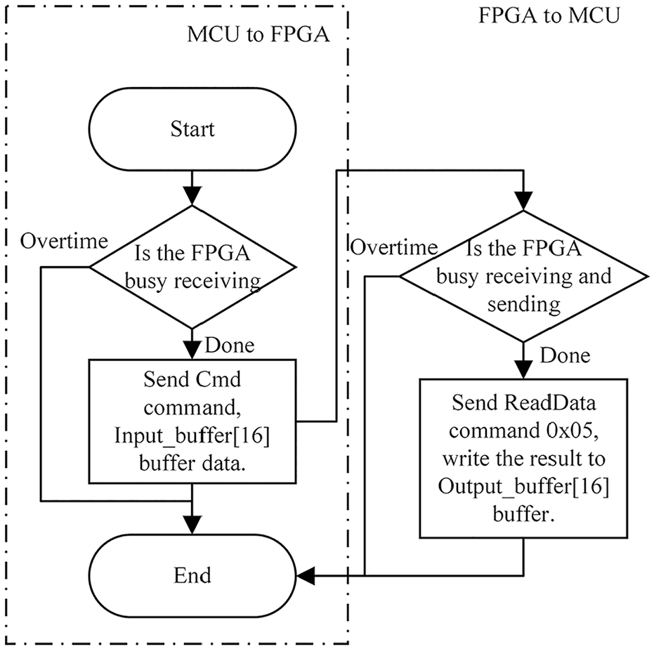
The schematic illustrates the process of writing a single data point to the FPGA and subsequently reading that data point back from the FPGA.
Algorithm design
Upon receipt of a single instruction frame from the PMU via the CAN bus, the system will start the on-orbit reconfiguration task. Firstly, it is necessary to ascertain whether the FPGA chip number in the instruction matches the number in the selected program package. If this is the case, the MCU will verify the integrity of the off-chip Flash packet. If the packet file passes the CRC check and the page CRC check, the FPGA will be updated on-rail. This will be signaled by the sending of an interactive frame to configure the FPGA into SPI Slave programing mode. The update will be complete when the mirrored packet is completely written to the FPGA. To the FPGA, the on-rail update is now complete. If the aforementioned steps have not been completed, it is imperative to halt the operation and enter the error code into the answer packet.
As shown in Figure 6, the SPI slave programing process is described as following.
Algorithm Initialization: Initialize the instruction Cmd, input buffer Input_buffer, output buffer Output_buffer, and check the off-chip flash connection status.
Read and Verify Mirror File Information: Read the image length, FPGA number, and other information according to the instruction frame address parameter. Then, totalize and verify the data packet by page (Flash 512 bytes per page) and by complete data packet.
ID Consistency Verification: Read the target FPGA ID code and the ID code of the mirrored packet in flash memory. Ensure all three IDs are consistent.
Read Bitstream Header: Retrieve the mirror bitstream CRC checksum, target FPGA ID, and the number of data stream blocks from the flash memory.
Read FPGA Configuration: The MCU transmits the Read buffer instruction (0x30) to the FPGA, reads the FPGA return value, and writes it to Output_buffer. The process is completed when all the information has been read.
Configure SPI: The MCU sends the SPI Programing Mode Setup instruction (0x06) to the FPGA to configure the SPI interface of the FPGA into programing mode, which can only be used to receive the bitstream.
Enable Programing Mode: The MCU sends the ISCEnable instruction (0x14) to the FPGA to enable ISP mode. The data stream received from the SPI interface is then programed into the FPGA’s internal non-volatile memory cells while the original program is stopped.
Write Data Stream: The MCU writes the data stream from the off-chip flash memory to the FPGA using the Input_buffer until all the data is written.
Exit Programing Mode: The MCU sends the ISCDisable instruction (0x15) to the FPGA, causing the FPGA to exit ISP mode and reset automatically.
Release SPI: The MCU sends the SPIRelease instruction (0x23) to the FPGA to release the SPI interface.
Verify SN Code Value: The MCU sends the ReadSN instruction (0x18) to the FPGA to read the FPGA device serial number. If the reading matches the preset value, the FPGA reconfiguration is considered successful. Otherwise, it is an exception and an error code is returned.
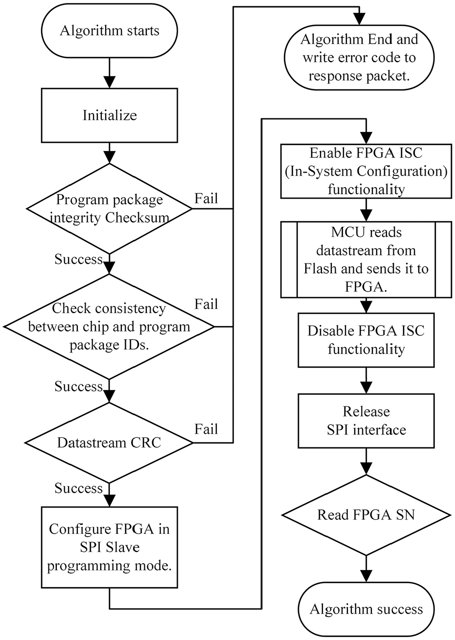
SPI slave programing flowchart.
The data stored in the flash memory is arranged on a page-by-page basis, with a single mirror packet occupying 16 flash sectors. Each sector contains 512 pages. Accordingly, the data can be accessed by querying the address information lookup table to obtain the offset address of each data block in the flash memory. The offset address is then used as the base address to read the flash data and transfer it to the FPGA through the input buffer. Furthermore, a data status check instruction is also sent to the FPGA after each frame of data writing. Subsequently, if the FPGA responds correctly, the next write is executed; otherwise, the reconfiguration operation is terminated. The data writing flowchart is illustrated in Figure 7.
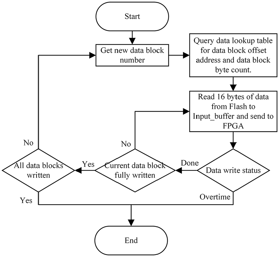
The MCU is responsible for reading data from the flash memory and writing it to the FPGA until all of the data has been transferred.
Reliability design
Since the DRO-A satellite will stay in the DRO orbit for a long time, in addition to selecting a high-reliability flash chip for the hardware, it also adopts a multiple-checking design at the software design level: when the GTM receives a bitstream packet, it will write the same data to three memories simultaneously by using triple-mode redundancy technology, which greatly reduces the risk of particle inversion.21–23 When a file needs to be read from Flash for reconstruction, three copies of data are read from three addresses for comparison, and the one with the highest number of occurrences is used. For the example shown in Figure 8, the value 0xFF is used.
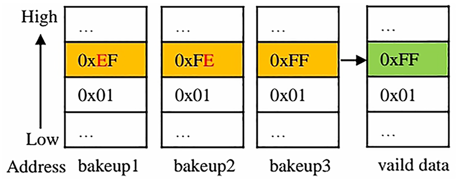
The bitstream file stored in the bakup1, bakup2 and bakeup3 memory should be identical. In the event of a data corruption incident, the correct data can be reconstructed from a comparison algorithm.
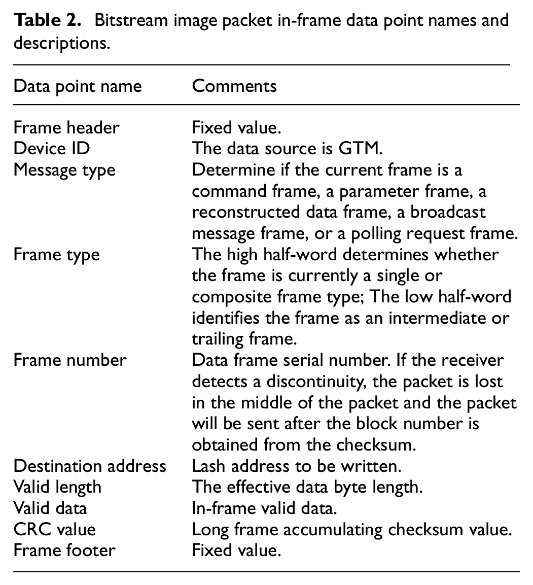
Due to the nature of the flash memory chip, it is necessary to erase the data by sector. If erroneous data is written, it is necessary to re-inject 256 kB data into a single sector. However, the bandwidth of deep space orbit data upload is constrained, necessitating an increase in the checksum design to prevent the occupation of additional bandwidth resulting from the writing of erroneous data. Consequently, the frame type, frame serial number, flash write address, and frame checksum value are incorporated into the data frame processing in the event of packet loss, code value flip, or code value loss. In such instances, the current data frame is discarded, and the lost data frame serial number is determined based on the error information in the answer packet. This allows for the current frame to be replenished, thereby reducing the number of data frame uploads. The detailed information in the message frames is presented in Table 2.
Bitstream image packet in-frame data point names and descriptions.
In the event of an anomaly during the on-orbit reconfiguration process, it is imperative to halt the reconfiguration immediately to prevent the erroneous execution of logic or control operations. This could potentially lead to damage to the equipment. The error code is logged and transmitted to the ground in such instances. The abnormalities that are included in the on-orbit reconfiguration process are as follows:
Satellite-Ground Transmission Anomaly: If the data frame writing address is outside the specified range, or if there are transmission errors or code value losses, the current frame is considered abnormal and will be discarded.
Complete Program Package Verification: The entire program package in Flash is verified if all data frames have been written or the sending command has been executed before track reconstruction. If the result is anomalous, it is deemed to be problematic.
Page-by-Page Program Package Verification: Verification of the program package in Flash should be conducted on a page-by-page basis when all data frames have been written or before sending commands for on-rail reconfiguration. If the result is abnormal, further investigation is required.
Three-Mode Redundancy Inconsistency: During the verification process of the program package, if the results of the three-mode redundancy comparison are inconsistent, an anomaly is detected.
Program Package ID and FPGA Chip ID Mismatch: During the program package verification process, if there is an inconsistency between the program package ID and the FPGA chip ID, an anomaly is detected.
CRC Check Anomaly: During the program package verification process, if the CRC16-CCITT check result of the data stream within the program package is found to be anomalous, it indicates a problem.
SPI Interface and FPGA Chip Connection Issue: During the algorithm’s execution, an abnormal connection between the SPI interface and the FPGA chip was observed, accompanied by a busy timeout status.
MCU and FPGA Chip Communication Issue: During data communication, if there is an issue with the communication between the MCU and the FPGA chip, it results in unsuccessful data writing.
Experimental setup and results
A ground test was conducted using GTM electrical parts, a payload ground test platform, a PC-side CAN ground test host computer simulation PMU for testing. The diagram of the test setup in shown in Figure 9. The subsequent GTM flight samples were utilized for platform electrical testing, satellite thermal experiments, and mechanical tests for reconfigurations, which were verified as successful.
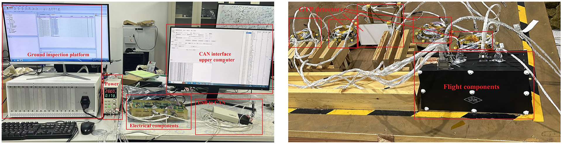
The left photo depicts the ground test of the load electrical component, while the right one illustrates the ground test of the load flight component.
The test process used the FPGA bitstream file and the ground processing program was processed as a mirror packet. The MCU will write the data packets sent from the ground inspection host computer through the CAN bus to its Flash memory, and it will return telemetry packets every second. It will then receive commands to perform on-orbit reconfiguration operations, during which the oscilloscope is used to test the waveforms of the SPI bus between the MCU and the FPGA. This will involve configuring the ISC_Enable mode of data interaction, for example, by testing the SPI interface CLK and CS, MOSI, and MISO three signal lines of the actual waveform. Figure 10 shows the signal waveforms of MCU and FPGA data interaction.
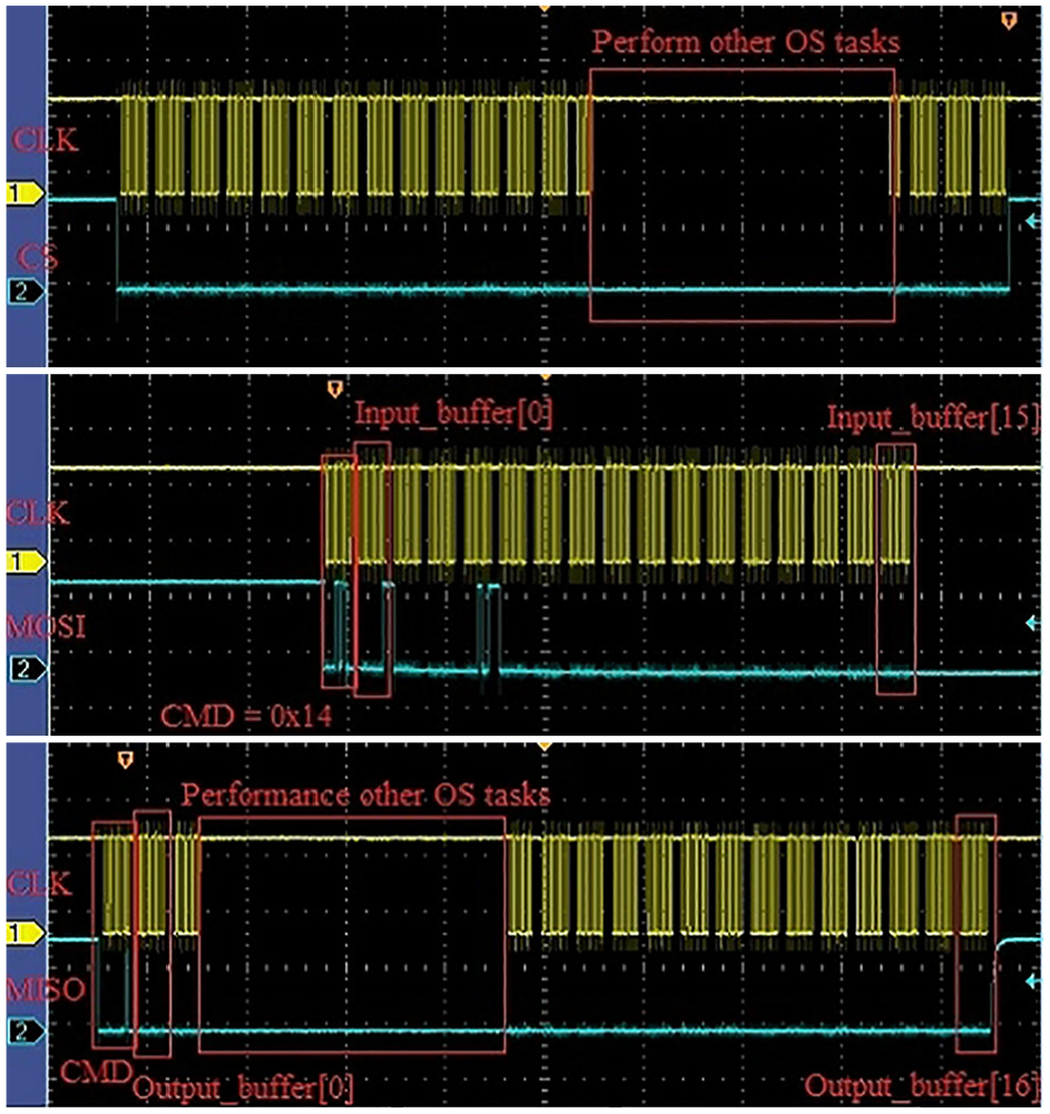
The signal waveforms of MCU and FPGA data interaction. Top: MCU pulls down the chip select line and selects FPGA. Middle: MCU sends data to FPGA, first byte is instruction 0x05. Bottom: the MCU reads the data returned by the FPGA. The discontinuous part of the picture indicates the program performing other tasks.
Upon reconstruction of the bitstream file using disparate versions, the trigger test was conducted by adjusting the thresholds and comparing the downstream merged data with the data within the trigger long-type message. A discrepancy of one second was observed between the two in the older version of the program, as illustrated in the top plot of Figure 11. In contrast, the newer version of the program exhibited a perfect match, as depicted in the bottom plot of Figure 11. The energy spectrum and binned data format of the GTM follow the scientific product data format of the GECAM satellite payload.
24
The
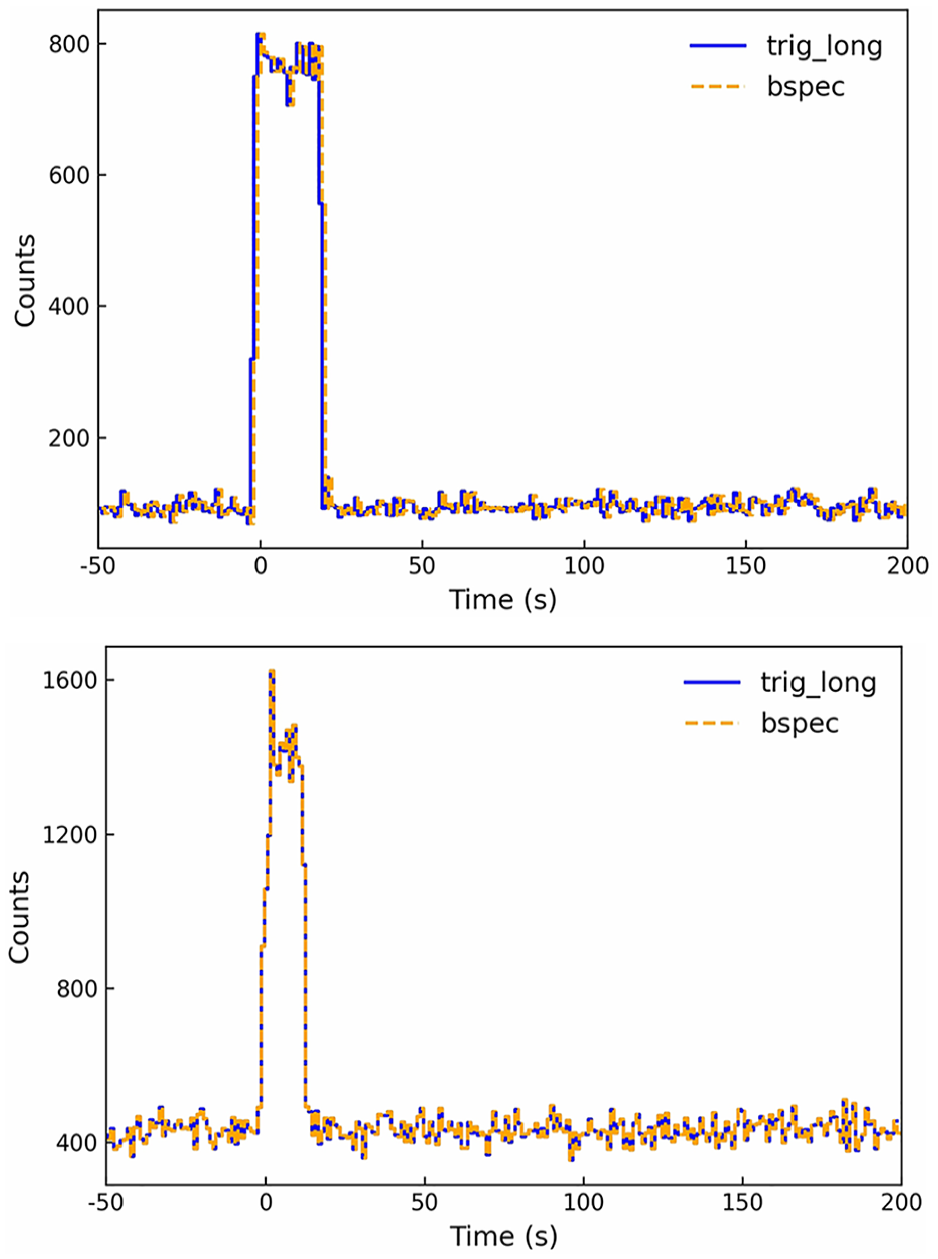
The horizontal axis represents time, with 0 marking the trigger time. The vertical axis shows the counts per second. The blue line represents the light curve plotted from the long-type trigger messages, while the orange line represents the binned spectral data. The consistency between these data validated the function.
Discussion
In this work, we proposed and implemented a novel design of GTM electronics to prevent anomalous caused by particle events in the deep space orbit. In addition to describe our method of FPGA reconfiguration, we also did a comparative analysis with other studies on spacecraft FPGA in the field of on-orbit reconstruction in terms of control architecture, speed, chip type, and other related factors, which is summarized in Table 3. Based on this comparison, we point out that innovation of our work is as following:
Equipped with Flash type FPGA chips, while using more widely used non-RAM types. Its process has a stronger anti-flipping ability and is loaded from the inside during startup, saving time from loading from PROM and refreshing circuit configuration.
By using the MCU as the main control chip, actively detect whether the operating current of the target FPGA is normal and reconstruct the FPGA at any time. During the reconstruction process, it can be paused and resumed. At the same time, it verifies that the backup data packet is correctly received and stored.
Using the SPI interface instead of JTAG (or Analog JTAG), a single FPGA occupies four IO pins, and only two new pins need to be added for each additional expansion.
The software algorithm used by the MCU adopts a short-frame interaction and response verification strategy. It writes a small amount of data at a time and performs frequent status checks on the data response to more accurately control the reprograming process.
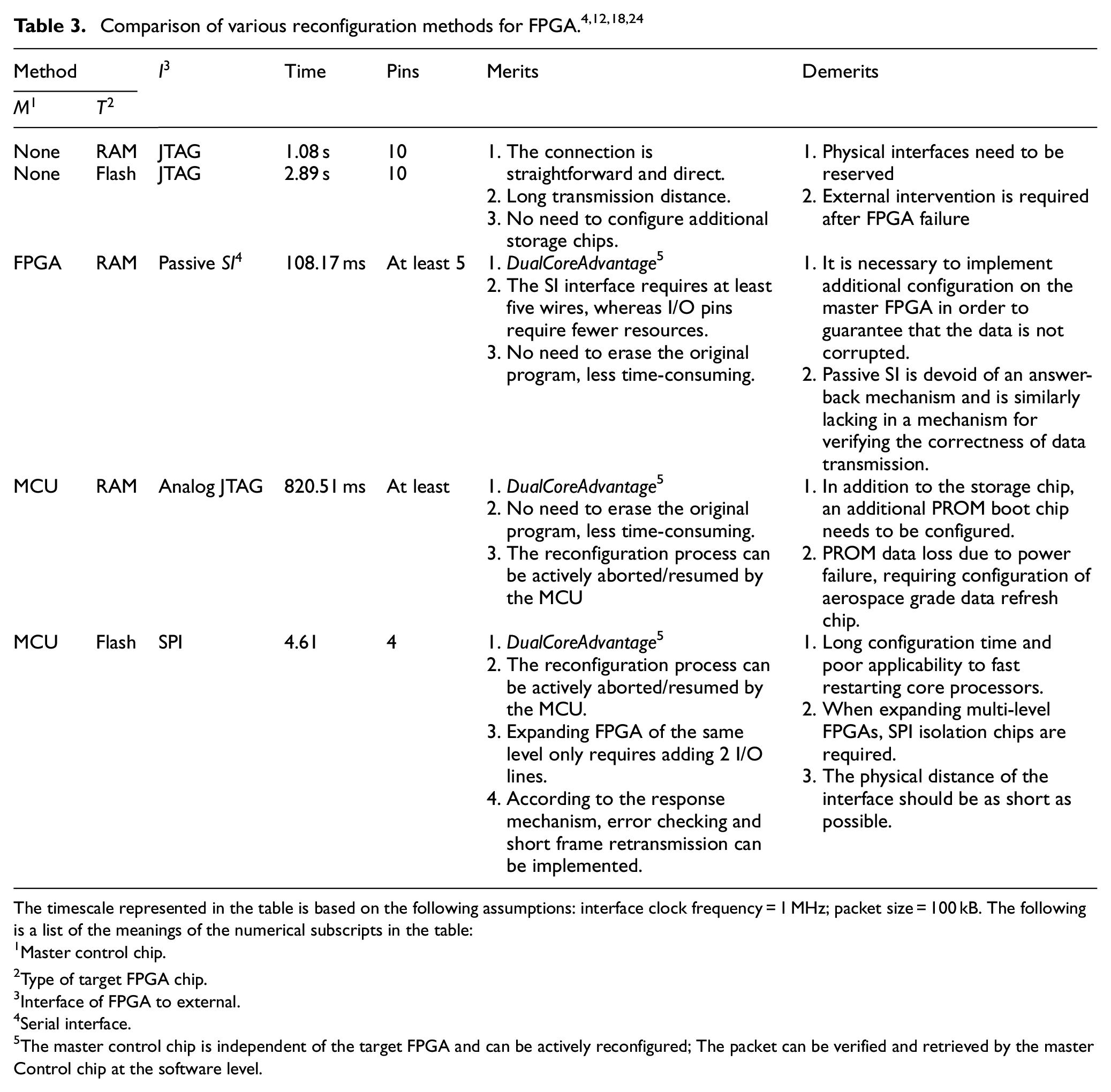
The timescale represented in the table is based on the following assumptions: interface clock frequency = 1 MHz; packet size = 100 kB. The following is a list of the meanings of the numerical subscripts in the table:
Master control chip.
Type of target FPGA chip.
Interface of FPGA to external.
Serial interface.
The master control chip is independent of the target FPGA and can be actively reconfigured; The packet can be verified and retrieved by the master Control chip at the software level.
In addition, the solution proposed in our work has the advantages of multiple error checks, interrupt continuation and ease of expansion. However, this solution requires approximately 4.61 s to reconfigure a 100 kB file size, making it unsuitable for onboard FPGAs that require rapid reconfiguration, such as central processing units in space stations/orbiting satellites (approximately 20 MB data packets, resulting in approximately 16 min of uncontrollable time). It is more suitable for peripheral payload devices, which typically have smaller data volumes, focus more on data reliability, and do not affect other devices.
Conclusion
To realize the reliability requirements of the GTM payload onboard the DRO-A satellite, we designed a high-reliability FPGA in-orbit reconfiguration scheme that reduces chip resource utilization compared to the traditional reconfiguration scheme. The focus is on the satellite-to-ground data transmission process and the integrity of data writing during ground tests. Reconfiguration of multiple FPGAs can be performed on-board by providing the original bitstream files of different versions of the FPGAs to the ground. In addition, the master FPGA can be used to extend the sub-FPGAs, allowing the sub-FPGAs to be updated on-orbit. Compared to other on-orbit reconfiguration techniques, the MCU-driven reconfiguration process can resume after an interruption and incorporates multiple checksums into the algorithm to ensure reliability. These features make it very useful for subsequent on-board FPGA on-orbit reconfiguration procedures.
Although our method is currently being used for small-scale FPGA reconstruction for payload in deep space orbit, it is applicable to all spacecrafts that rely on on-board storage verification rather than frequent program updates, as well as space payloads with relatively broad configuration time requirements rather than central processing units, such as spacecraft peripheral payloads passing through the SAA area or radiation belt near the Earth. By introducing compression and decoding designs for data packets, our design can be further optimized, which will help reduce storage requirements, improve transmission efficiency, and reduce reconfiguration time.
Footnotes
Appendix
Declaration of conflicting interests
The author(s) declared no potential conflicts of interest with respect to the research, authorship, and/or publication of this article.
Funding
The author(s) disclosed receipt of the following financial support for the research, authorship, and/or publication of this article: This project is supported by the National Natural Science Foundation of China (Grant No. 12173038, 12273042) and the Strategic Priority Research Program, the Chinese Academy of Sciences (Grant Nos. XDA30050100, XDA15360102, XDB0550300).
Ethical considerations
Not applicable
Consent to participate
Not applicable
Consent for publication
Not applicable
Data availability statement
Data sharing not applicable to this article as no datasets were generated or analyzed during the current study.