
Abstract
In this study, a battery management system was implemented using the passive charge balancing method. The battery system was created with lithium ion battery cells commonly used in electric vehicles. Two main microprocessors were used as a master and slave for the management system. An STM32f103C8 microcontroller was used as a master, and a PIC18f4520 microcontroller was used as slave control units in the battery management system. Charge control of a battery pack consisting of four cells was performed. The information received from the current and voltage sensors was collected from each cell using a slave controller and sent smoothly to the master controller system. These experimental results indicated that the passive balancing method was implemented and the battery cells were charged successfully. The proposed method was applied to battery pack consisting of a four-cell LiFePO4 battery with a capacity of 40 Ah. This work incorporated original situation that have not been realized before. A digital to analog converter circuit was created using a buck converter topology. Thus, the MOSFET was used as an adjustable resistance. Also, it was one of the first studies in which the MOSFET was used as a regulated resistor in battery management systems.
Introduction
Today, with the increasing pollution of the environment and increasing population density, in many areas, human beings are searching for systems that do not harm the environment. A lot of work has been done on the development of more environmentally friendly electric vehicles due to the harmful effects of internal combustion engines.1–3 This class of electric vehicles also includes autonomous and unmanned electric vehicles that are lower power than standard electric vehicles. When studies on electric vehicles are examined, it is seen that most of the problems experienced are related to batteries. The problems experienced by the batteries due to their limited lifetime and their warming are among the important problems to be solved. The solution of these problems is directly related to the control management of the batteries. Therefore, an effective battery management system (BMS) is needed to increase the performance and extend the life of battery technologies.4–6
The automotive industry has made significant investments in electric vehicle technology because of problems such as the dependence on oil, environmental pollution, and energy consumption among existing vehicle technologies. So, it is predicted that the number of electric vehicles will increase in the future. Thus, the work to be done for the BMSs of the vehicles will become even more important. Batteries vary according to the materials they contain, so it is possible to find more than one type of battery.
PbAc (lead-acid), 7 NiCd (nickel cadmium), 8 NiMH (nickel metal hydrate), 9 and Li-ion (lithium ion) 10 battery types are generally used in vehicle battery technology. Compared to other battery technologies, lithium ion batteries are preferred because they have significant advantages such as a high rated voltage, high energy density, long life, and no memory effect.11,12 Uncontrolled use of batteries in electric vehicles can cause serious damage. For this reason, the BMS is used in electric vehicles for controlling the batteries.13–15
In the BMS field, many studies have been performed, and different methods have been applied to the battery cells for charging batteries more smoothly. The battery balancing method is one of the most frequently used methods in BMS applications. The cell balancing methods can be separated into two main topics as passive and active balancing. 16
When the studies in the literature are examined, it is seen that passive balancing methods are applied in two different ways.
The first is the fixed shunt resistor. This method uses a resistance which is connected continuously to the battery cell. This resistance is used for by passing the current for all the cells, and the resistor is adjusted to limit the cells voltage. The second is the controlled shunting resistor, which is based on removing the excess energy from the higher cells to consume it on the resistor with the controlled switches/relays. 17
A shunting resistor based on the balancing method was investigated, and sealed relays were used for switching process. With this technique, the sealed relays provided much faster equalization and higher efficiency. 18
Usually, the passive method disposes of some electric charge from an overcharged cell through the resistor element until the battery cell voltage level matches the state of charge (SoC) reference or voltage reference value.16–18
For the passive balancing operation, high-power stone resistors are generally used. These stone resistors take up a lot of space in the circuits due to their large dimensions. This is a problem because of the limited placement area.
To solve this problem, it is possible to use the MOSFET in battery balancing operations by taking advantage of its ability to be used as a resistor. 19 The balancing current can be adjusted as desired by connecting the balancing resistor combined with an internal resistance of the MOSFET. So, an internal resistance of the MOSFET is used as the balancing resistor. Thus, the balancing current can be adjusted within the desired limits.20,21
Compared to the previous paper, in this paper, the BMS design has been implemented using ARM and PIC based microprocessors. Control operations were performed using semiconductor MOSFET elements. In addition to its use in the control process, MOSFET is also used directly as a balancing resistance. The stone resistance above the balancing circuit is intended to limit the balancing current. The excess energy between the battery cells was dissipated on the MOSFET as heat by driving the MOSFET in linear mode. This ensured that the cells were smoothly charged. At the same time, MOSFET takes less space in the battery charge control circuit than stone resistance. So, it will be possible to design the control cards in a smaller size. Moreover, a digital to analog converter (DAC) circuit created with a buck converter topology was designed to operate the MOSFET in linear mode. The designed DAC circuit is not included in the literature and not used in any system. Also, this study is one of the first studies based on MOSFET’s linear mode control about battery charge control circuits topic in the literature. In this way, the MOSFET can be used as a regulated resistor by adjusting the duty ratio of the PWM (pulse width modulation) signal. Two main microprocessors were used as a master and slave for the management system. The two circuits were very close to the battery cells, so the cable tie that connected the circuits to the battery cells was very short. Thus, the cable losses that would cause problems in reading analog data were avoided. The modular design facilitated the mounting of the BMS circuits on the battery.
MOSFET linear mode operation
MOSFETs are mainly used in switching applications such as DC/DC converters and motor control using PWM. MOSFETs can be operated in the cut-off, linear, or saturation region by applying the relevant voltages of its terminals. 22
Figure 1 shows the typical output characteristics of an n-channel power MOSFET in which the different modes of operation are shown. In the cut-off region, the gate-source voltage (VGS) is less than the gate-threshold voltage (VGS(th)) and the device is an open-circuit or off. In the Ohmic region, the device acts as a resistor with an almost constant resistance RDS(on) and is equal to Vds/Ids. In the linear mode of operation, the device operates in the ‘Current-Saturated’ region where the drain current (Ids) is a function of the gate-source voltage (Vgs). 24
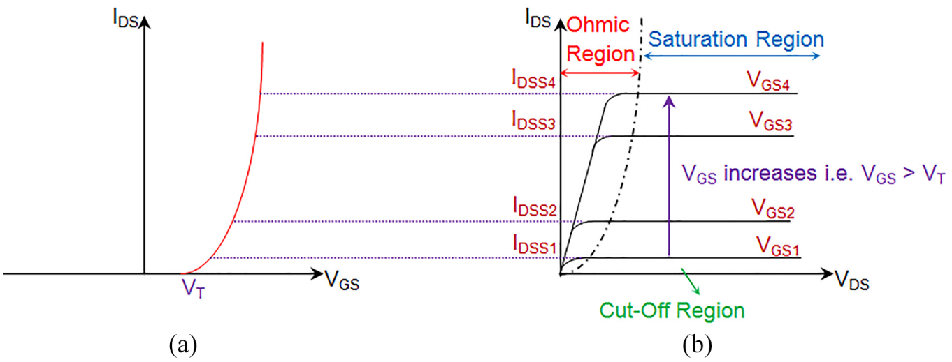
(a) Transfer characteristics of n-channel enhancement-type MOSFETs and (b) MOSFETs’ operation regions. 23
The linear mode of the MOSFET operation should not be confused with the linear region. In this region, the MOSFET drain current is a linear function of the drain voltage. The linear mode of operation is defined as when small changes of VGS result in linear changes of the drain to the source current. The IDS current then depends directly on the VGS voltage of the MOSFET. In linear mode operation, MOSFETs are generally used at the battery charger, fan controller, e-fuse, load-switch, buck converter, and general switching applications. However, the MOSFET is not a very popular application to use as a load.The SOA (safe operating area) chart needs to be consulted in order to determine the MOSFET’s working capacity as a load. 21
For instance, for a 10-ms wide pulse, a MOSFET could support 100 V from drain to source with nearly 25 A flowing through it. This equates to a power dissipation of 2500 W.
In Figure 2, static DC operation area limits are determined as the ‘DC’ line. The use of the MOSFET as a load is more secure in this region. The MOSFET with the lowest RDS(on) takes the highest proportion of the current and dissipates the most power on the MOSFET (power dissipation P = VDS × ID).
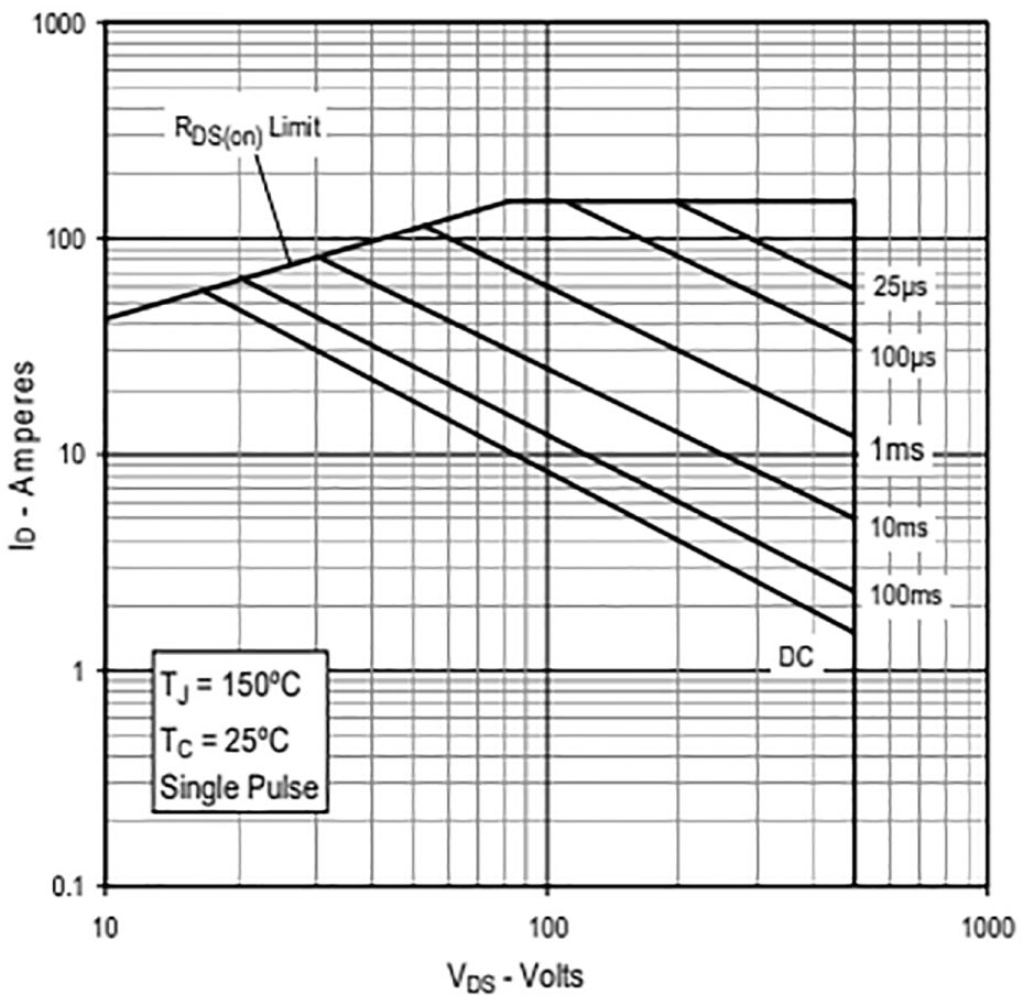
IXTK60N50L2 safe operating area. 25
Passive control circuit
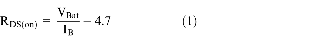
The passive balancing technique was used to control the voltage of the battery cells. In passive control methods, excess voltage between cells is spent as heat over the stone resistance. A passive control circuit can be seen in Figure 3. L1 inductance, C10 capacitance, and D1 diode were used to generate the output filter based on the buck converter topology. In fact, considering the operating logic of the circuit, a DAC circuit is created here. Normally, the input signal is applied as PWM. The signal can be obtained from the DAC circuit output as a variable constant voltage according to the duty cycle of the PWM signal. Thus, a variable and constant voltage can be applied to the Gate terminal of the MOSFET. In this way, the MOSFET is switched in the linear region and the voltage of the Gate terminal (VGS) can be adjusted by this method.The current value was calculated by taking the differences of the voltages falling on the resistance legs using the stone resistance in the circuit without using the current sensor. The MOSFET was used as a regulated resistor by applying the constant voltage value from the buck converter to the gate of the MOSFET. Thus, the excess voltage was spent on the MOSFET.
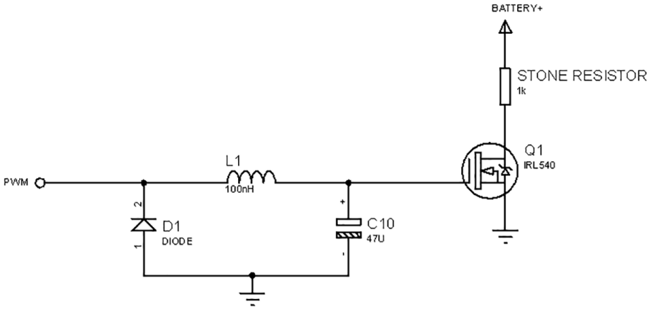
Passive control circuit.
Designed BMS system overview
BMS circuits were designed and manufactured for LiFePO4 battery cells. The BMS circuits produced were placed on the battery cells and the BMS application was carried out.
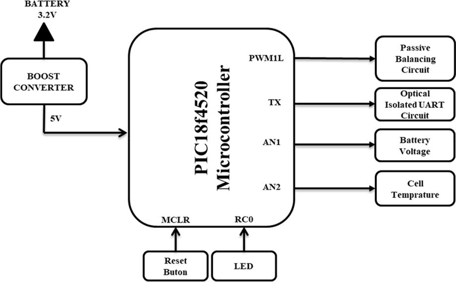
Because there is more than one battery in this application, master and slave controller systems were designed to work together instead of a centralized system. The slave controller module includes a passive control circuit. The charge of the battery module controlled with the master controller. First, the slave module gathered voltage and current data from the four battery cells. After this process, all the data were sent to the master controller using the UART (universal asynchronous receiver-transmitter) communication system. The battery cell voltages, current and temperature values can be read at high resolution. The designed and implemented BMS control system block schema can be seen in Figure 4.
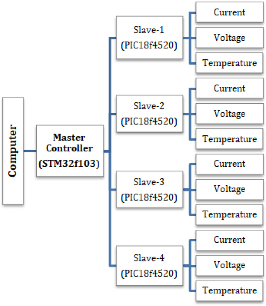
Battery management system overview.
BMS slave and master control card design
Healthy and long-term operation of the designed circuits may vary according to the production type. It is important to this work that the designed circuit is for continuous and long-term operation.
PCB design using surface mounting technique and through-hole technique
There are two types of mounting techniques in the industrial designs for electrical circuits. Through-hole and surface mounting techniques (SMT) are commonly used.
The slave controller circuit was implemented using SMT and through-hole techniques. During this design process, the Proteus programme was used. SMT circuit components were used, so a compact card design was made. A PIC18f4550 SMT-type microcontroller was mounted at the bottom of the designed circuit card. The BMS slave controller circuit Proteus programme design can be seen in Figure 5(a). The slave controller circuit’s front and back views are shown in Figure 5(b) and (c).
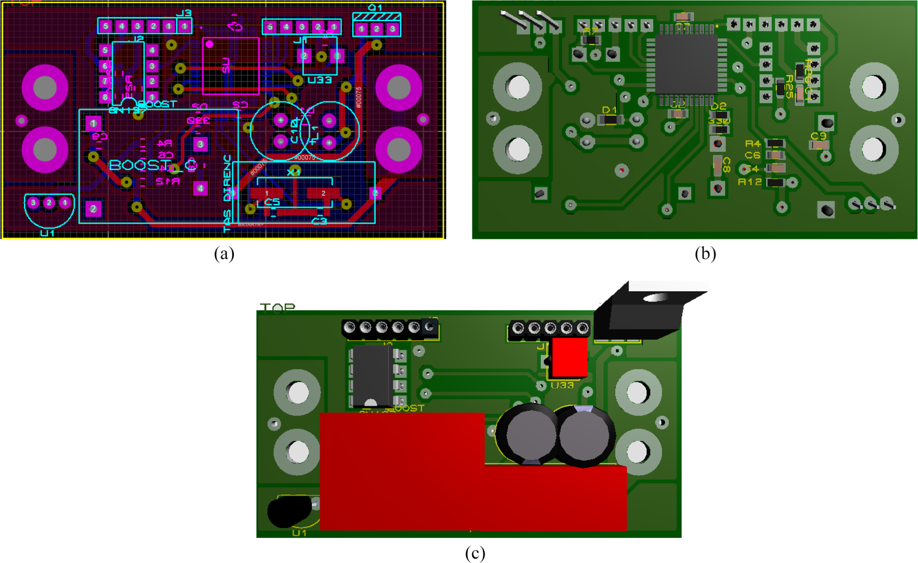
Slave controller card: (a) Proteus design, (b) bottom side, and (c) top side of slave controller.
Slave control card
The slave control card consisted of a boost, passive balancing, serial communication and measurement circuit. In order to operate the PIC18f4520 microprocessor integrated in the slave control system, the 3.2 to 3.3-V value was increased to 5 V using the boost converter circuit.
The passive balancing circut consisted of a MOSFET, 4.7-ohm stone resistor, and filtering components. When the battery system needed a balancing operation, the current flow on the stone resistor was adjusted according to the voltage difference between the two battery cells. By setting the PWM duty ratio according to the voltage difference between battery cells, the current value to be passed through the stone resistance was determined. So, with this process, excess voltage was used as heat on the stone resistance, and the cells were balanced.
The values of the voltage, current, and temperature data collected via the measurement circuit were sent to the master processor via the serial communication port. A current sensor was not used for current measurement in this system. First, the voltage difference between the stone resistance of two connection points was determined. The current value was obtained by dividing the determining voltage value by the stone resistance value. The battery voltage value was determined by voltage divider resistors, and an LM35 sensor was used for the temperature value.
The designed circuit was equipped with a reset button and an LED to indicate whether the system was working or not. The designed and implemented slave control system block schema can be seen in Figure 6.
BMS slave control card block schema.
Master control card
A slave controller card connects to a battery cell and reads the current, voltage, and temperature values of the battery cell and sends these values to the master controller circuit.The STM32f103 microprocessor was used as the master card controller. According to the data received from the slave cards, it was determined which cells were to be balanced. Cell voltage and current information was sent to the computer interface by the master control unit.
BMS algorithms
There were two different algorithms applied to the BMS. The master controller algorithm can be seen in Figure 7. According to Figure 7, first, initial adjustments are performed for the interrupt and serial communication. When the master controller is ready for the reading and writing process, communication is started. The master controller takes all the battery cell voltage, current, and temperature information completely with serial reading. After this operation, these data are sent to the computer interface. The minimum and maximum voltage battery cells are determined for balancing. If the difference of the voltage value of two cells is more than 50 mV, a balancing operation starts for equalization. Otherwise, the algorithm continues before the data reading process. At the same time, the cells’ temperature is controlled by the master controller. If one of the cell temperatures is higer than the maximum temperature value, this cell charging process is stopped. The slave controller card algorithm is given in Figure 8. According to the algorithm of the slave controller, initial adjustments are performed for the interrupt and serial communication processes. If there is a command coming from the master controller related to the need for a balancing process, then the MOSFET is switched using the PWM duty ratio. Voltage, current, and temperature data are read for sending to the master controller.
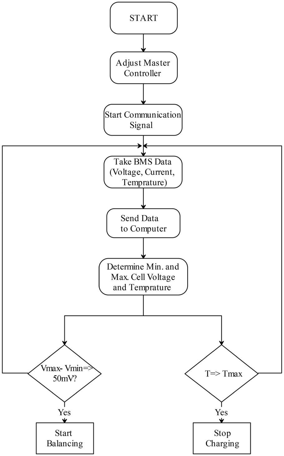
BMS master controller algorithm schema.
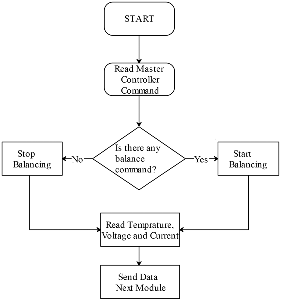
BMS slave controller algorithm schema.
Experimental results and discussion
First, the battery module group was supplied from a DC source to provide charging. The value of each cell charge was different. At this point, the designed BMS system started the balancing process for each cell. The lowest voltage level of the battery cell was determined according to the designed algorithm. The voltage differences of the other cells were measured according to this voltage value. Then, when balancing was required, the overvoltage of the cell was reduced to the lowest voltage level. Excess energy was spent on stone resistance, so the overvoltage decreased with this method.
The installed state of the BMS system is shown in Figure 9. As shown, the slave controller for each cell and the master controller that controls these controllers are connected.
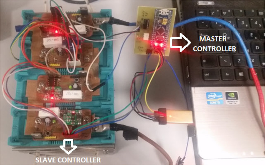
BMS control system and batteries.
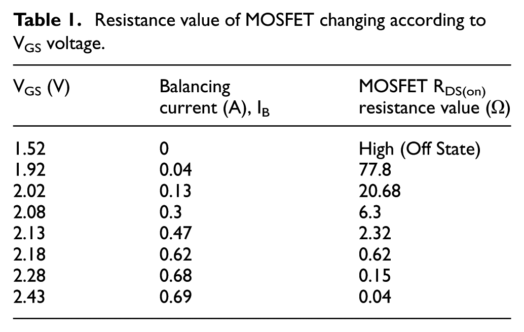
The balancing current of one battery cell, VGS voltage, and obtained MOSFET RDS values are given in Table 1. The resistance values were determined under this condition of that battery supply voltage was measured as constant 3.3 V (VBat). When VGS voltage is 1.52 V, the MOSFET is expressed as Off State. It is seen that RDS resistance decreases with increasing voltage of VGS at Table 1. The MOSFET is on mode when VGS voltage is 2.43 V, the resistance value is measured as 0.04 Ω. IRL540N-type MOSFET was used at BMS control card. In addition, this MOSFET RDS(on) resistance value was determined as 0.04 Ω at its datasheet. Here, it is understood that MOSFET is completely open when 2.43 V is applied. A 4.7-Ω stone resistor was used to limit the current in the passive charge control circuit. It is important to state that this value should be taken into account when calculating the resistance value of MOSFET. The RDS(on) values in Table 1 were calculated according to equation (1)
Resistance value of MOSFET changing according to VGS voltage.
The voltage values taken from output of the DAC filter circuit are shown in Figure 10 when the voltage values of these signals are 2.02 and 2.43 V. These voltage signals are applied to the Gate terminal of the MOSFET. When these signals are applied, the current flowing through the MOSFET is 0.13 and 0.69 A, respectively. Also MOSFET resistance values were determined as 20.68 and 0.04 Ω, respectively.
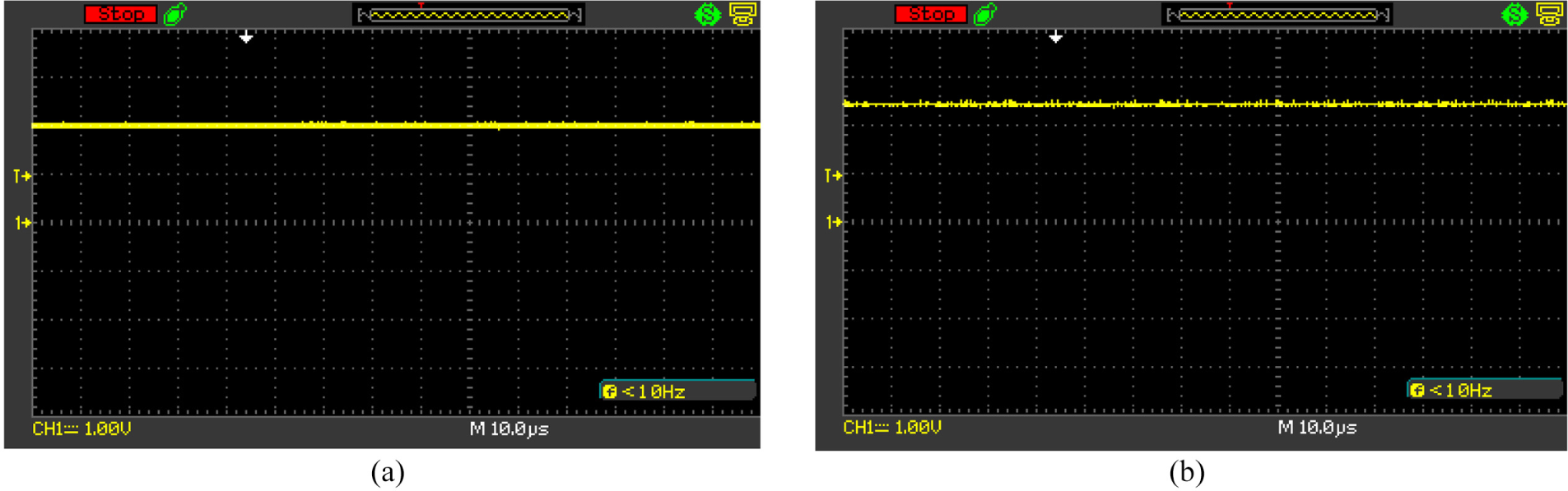
Signal from DAC filter output applied to MOSFET Gate Terminal: (a) VGS = 2.02 V, balancing current = 0.13 A, RDS = 10.8 Ω. (b) VGS = 2.43 V, balancing current = 0.69 A, RDS = 0.04 Ω.
The voltage values of the four cells are shown in Figure 11 when the batteries are being charged. The balancing system allows the cells to be charged together. Initially, the charge voltage starts at 3.4 V for a period of about 20 min, and all the cells were charged in a passive balancing technique to 3.7 V.
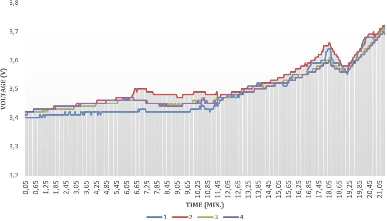
Batteries voltage values.
The balancing currents passed from the system during the charging process of the battery cells are given in Figure 12. The balancing currents are limited to 700 mA using the stone resistance.
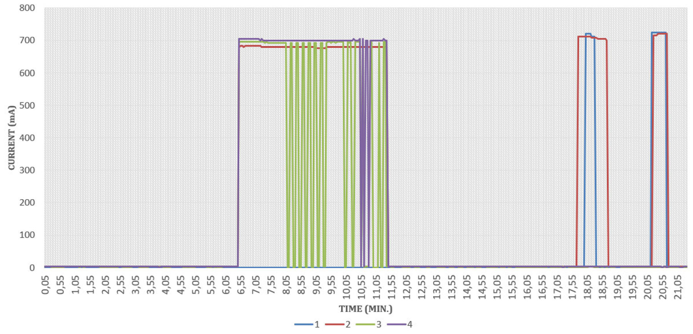
Batteries balancing currents.
The four-numbered battery cell removes a voltage imbalance between cells with a 700-mA balancing current. It is seen that the balancing current occurs when voltage imbalance occurs at different times. It is seen from Figure 12 that the balancing current of the second, third, and fourth batteries flow at the same time in 6.55th minute. The balancing current was measured approximately 700 mA. At this time, the balancing current of the first battery cell is 0 mA. The change in the balance currents of the third and fourth battery cells between 8.05 and 11.55 min is shown in the same figure. At this time interval, it is seen from the results that the balancing current of the second cell is constant around 700 mA. It is seen that the balance of the first cell flows at 700 mA at 18 and 20 min.
The interface for observing the voltage levels and balancing currents of the cell is shown in Figure 13. By means of the designed interface, the charge balance state of each battery cell can be checked, and a possible problem can be solved beforehand. Initially, the second cell has the highest voltage value of 3.5 V while the first cell has the lowest voltage value of 3.40 V, and a 120-mA balancing current is observed at the second cell because of its higher voltage level than other cells. Average temperature values were determined as between 26 and 32 °C at the end of this charging period. The initial temperature of the charging process was set at 26 °C. Towards the end of charging, the temperature value was observed up to 32 °C.
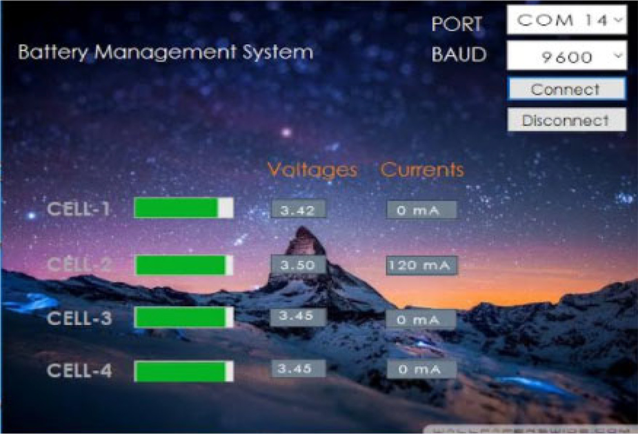
BMS system interface.
The advantages and disadvantages of the control methods are determined by evaluating over many factors. When the studies in the literature are examined, there are a few studies comparing active and passive studies. In some studies, it is stated that active balancing method–based studies are appropriate in BMS systems for electric vehicles. 26 However, these studies generally evaluate systems according to a few parameters. In a more general analysis, including more parameters, it is stated that passive methods can also be used for electric vehicles. In fact, when evaluated according to these studies, it is seen that passive-based methods are more appropriate than active balancing methods in terms of applicability. 27
Conclusion
This paper presented a passive control approach for an integrated BMS system using a modular Li-ion battery to achieve battery management. The BMS provides differential control of the battery cells using the master and slave controller logic and provides an opportunity for advanced battery management to achieve longer battery life and higher power limits. Experimental results were presented for a prototype system consisting of four series connected 40-Ah LiFePo4 battery cells. The battery cells’ voltage and current data were sent with serial communication to the computer interface. At the same time, the voltage levels of the batteries could be monitored from the computer. The implemented BMS control approach constitutes the infrastructure for future work.
Footnotes
Declaration of conflicting interests
The author(s) declared no potential conflicts of interest with respect to the research, authorship, and/or publication of this article.
Funding
The author(s) received no financial support for the research, authorship, and/or publication of this article.