
Abstract
High temperature occurs in testing of complex System-on-Chip designs and it may become a critical concern to be carefully taken into account with continual development in Very Large Scale Integration technology. Peak temperature significantly affects the reliability and the performance of the chip. So it is essential to minimize the peak temperature of the chip. Heat generation by power consumption and heat dissipation to the surrounding blocks are the two prominent factors for the peak temperature. Power consumption can be minimized by a careful mapping of don’t cares in precomputed test set. However, it does not provide the solution to peak temperature minimization because the non-uniformity in spatial power distribution may create localized heating event called “hotspot.” The peak temperature on the hotspot is minimized by Genetic Algorithm–based don’t care filling technique that reduces the non-uniformity in spatial power distribution within the circuit under test while maintaining the overall power consumption at a lower level. Experimental results on ISCAS89 benchmark circuits demonstrate that 6%–28% peak temperature reduction can be achieved.
Keywords
Introduction
The rapid progression of semiconductor manufacturing technology has enabled the design and development of highly complex system-on-chip (SoC) designs. However, this evolution has posed challenges to the test community. The continued shrinking of the transistor size has increased the probability of manufacturing defects in the integrated circuits (ICs). When a system becomes more complicated, the testing process becomes more challenging. Power consumption during testing has been significantly higher compared to the normal operation mode due to substantially increased switching activity.1,2 The power density of the ICs has been steadily growing simply because the number of transistors integrated into the silicon die has increased. The elevated levels of power density during test inherently increase overall circuit temperature and, at the same time, create localized heating events, called hotspots.3,4 Peak temperature on hotspot significantly leads to a high cooling cost, a decrease in reliability or even permanent damage.
Early research efforts about low-power solutions fall into two categories: core-level design for testability (DFT) and system-level DFT. 5 Consequently, traditional classes of low-power solutions targeting both methods have been proposed. Techniques falling in the former category include low-power scan architectures with gated clocks,6,7 scan cell and test pattern reordering,8,9 and low-transition test pattern generation algorithms. 10 This category consists of reordering techniques that reduce the switching activity by modifying the test vector order or the scan cell order. The latter is mainly based on power-constrained test scheduling algorithms.11–20 The system-level DFT limits the concurrency of the core tests based on a chip-level maximum allowable power limit. The power minimization problem is oriented toward reducing the switching activity in the circuit so that the dynamic power can be controlled. Although minimizing power consumption may reduce the overall temperature of the circuit under test (CUT), it is not effective enough in providing the best solution for peak temperature minimization on hotspots. Majority of these techniques failed to create spatially uniform temperature distribution due to non-uniform spatial power distribution.
In this paper, the importance of achieving spatial uniformity in temperature distribution and reducing the peak temperature is discussed. The temperature of a block depends on its own power density, as well as the heat transfer or heat exchange between the neighboring blocks. When the power consumption is uniformly distributed across the chip, thermal variance across the chip can be minimized. Therefore, genetic algorithm (GA)-based framework is proposed to fill don’t care bits in test patterns in such a way that both thermal variance across the chip and peak temperature are minimized.
The remainder of this paper is organized as follows. Section “Background and related work” reviews the background and related works. In section “Thermal modeling,” the thermal model is presented. The proposed GA-based thermal-aware don’t care filling algorithm is described in section “GA for thermal-aware patterns.” Experimental results of several ISCAS89 benchmark circuits are discussed in section “Results and discussion.” In section “Conclusion,” the conclusions are summarized.
Background and related work
Many low-power test generation techniques have been extensively investigated to minimize the power consumption during testing. However, the limiting power dissipation cannot alone guarantee against thermal hotspots. So power-aware testing has failed to solve the limitations. In order to solve the problem, thermal-aware strategies have to be developed.
Peak-temperature aware scan-vector optimization (PEAKASO) algorithm of Cho and Pan 3 minimizes the peak temperature by scan vector reordering based on overheat pre-compensation. They proposed a window-based power analysis to predict hotspots in the CUT by considering power consumption of the block and its neighboring blocks. The peak temperature on the hotspot is minimized by ordering high-power-consuming patterns earlier to maximize the heat dissipation, reducing the heat generation and pre-compensating the overheat.
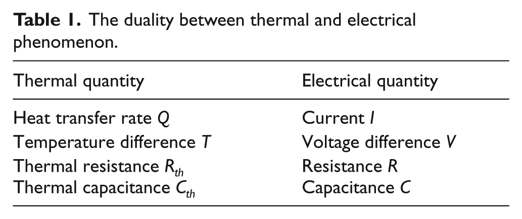
Rosinger et al. 18 proposed a thermo-resistance model as a guide for test scheduling. They used the RC-equivalent (Resistance-Capacitance) architecture-level thermal model from Skadron et al. 21 which makes use of the duality between the thermal and electrical phenomena. They only considered the lateral flow of heat from an active core by reducing a chip into a network of thermal resistances and thermal capacitances. The proposed test scheduling method used a clique cover algorithm over a resource conflict graph (RCG) to obtain thermal-safe test sessions. They computed thermal profiles quickly but with less accuracy.
The technique proposed by Rosinger et al. 5 computes short thermal-safe test schedules. The authors suggested an approach that utilizes the core adjacency information to guide test scheduling. They also indicated that the non-uniform distribution of the heat results in hotspot on the die. Although the methods proposed in Cho and Pan 3 and Rosinger et al. 5 reduce the peak temperature on the hotspots, the temperature differences within the circuit range from 40 °C to 50 °C. The method is computationally expensive for complex systems.
Yoneda et al. 22 proposed a thermal uniformity–aware X-filling technique to achieve a spatial uniform temperature distribution for high-quality at-speed testing. The objective of the method is to minimize the statistical variation in power density for each test pattern among the circuit blocks. They also proposed a test pattern reordering technique 23 that reduces the temporal temperature variation while maintaining the spatial temperature variation by their earlier method.
Dutta et al. 24 proposed a thermal-aware X-filling technique that properly assigns logic values to the X-bits to minimize the peak temperature as well as the thermal variance across the chip.
Thermal modeling
Thermal modeling techniques can estimate the temperature of a chip. There exists a well-known duality between heat transfer and electrical phenomena presented in Skadron et al. 21 The heat transfer in a system can take place in three modes such as conduction, convection and radiation. In the electronic components, heat usually propagates through conduction which is assumed to be one dimensional (1D; Figure 1).
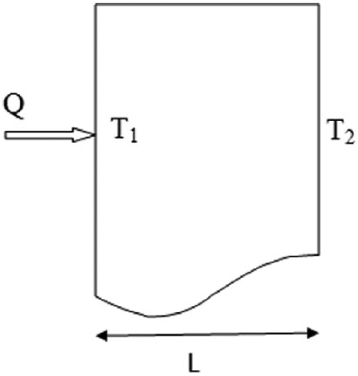
One-dimensional heat conduction flow.
The 1D heat conduction in a homogeneous isotropic material is described as
where q is the heat flux in W/m2, k is the thermal conductivity of the material in W/m K and T is the temperature in K. The heat flux is directly proportional to the temperature gradient at that point. The negative sign indicates that the heat flows in the direction of decreasing temperature.
Equation (1) can be rewritten as
where
There is a resemblance between equation (3) and Ohm’s law in circuit theory
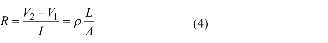
Heat conduction is also a transient process. The temperature distribution of an IC is governed by the heat conduction equation
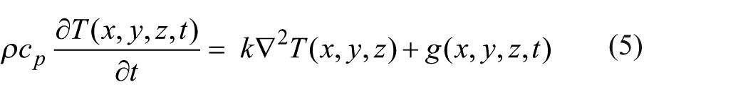
where T refers to variation in temperature with respect to time (K), ρ specifies material density (kg/m3), k denotes thermal conductivity (W/m K), g represents volume power density parameter depending on time (W/m3) and cp is the specific heat (J/kg K). Both g and k are assumed as constants. Equation (5) can be written in 1D form and can be integrated on both sides by x from 0 to L
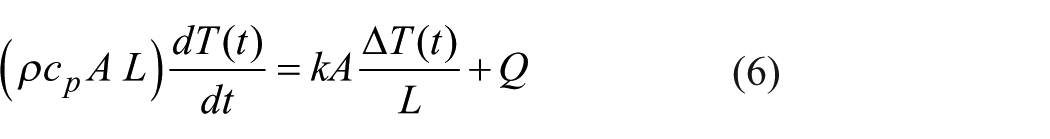
where ΔT = T2 – T1. The first term of the right-hand side of equation (6) is the heat transferred through thermal resistance. The equation can be rearranged as
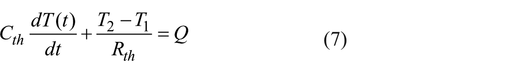
where
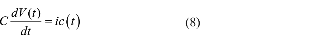
Thermal capacitance is the capability of the material to absorb heat, while electrical capacitance is the capacity of the material to store electrical charge. Equation (7) states that the total heat flowing through the material is equal to the sum of the heat flowing through the thermal capacitance (the alternative current (AC) component) and the heat flowing through the thermal resistance (the direct current (DC) component; Table 1).
The duality between thermal and electrical phenomenon.
Using thermal resistance and thermal capacitance of each sub-block in the package, an equivalent electric circuit is derived from modeling the dynamic heat flow in the chip. The dissipated power and layout (floor plan) information of the blocks is given as an input to the thermal model at every time step. The average temperature of each block over the time interval is estimated using computational methods.
GA for thermal-aware patterns
GAs 25 constitute a class of heuristic search and optimization techniques based on the principles of natural selection and genetics. They have been applied in various domains that are traditionally difficult to optimize. GAs can identify globally optimal or suboptimal solutions within reasonable time and computational cost. GA handles a population of potential solutions to a given problem. Each represents a possible solution (chromosome) to the problem and is evaluated by a fitness function to assess its competence to survive in the next generation. The fittest chromosomes are given opportunities to reproduce with individuals in the population. This produces new individuals as “offspring.” As this process continues, a sequence of successive generations evolves, and the average fitness of the chromosomes tends to increase until the termination criterion is satisfied. Since highly fit individuals are more likely to be selected as parents, the most promising areas of the search space are explored. If the GA has been designed correctly, the population will converge to an optimal solution to the problem.
Since the objective of the problem is to minimize the peak temperature of the circuit during testing, the power density variance across the block is found and tried to be minimized. The large test set with reasonable don’t care bits generated using MinTest 26 is taken as an input for testing the CUT. The GA is useful when the search space is very large. So, GA is chosen for the problem of finding an appropriate filling of the don’t care bits which will lead to peak temperature reduction.
In order to apply a GA for peak temperature reduction and thermal variation reduction, it is necessary to define an individual solution representation, selection procedure, crossover operator, mutation operator and fitness function. The GA procedure is outlined in Figure 2.
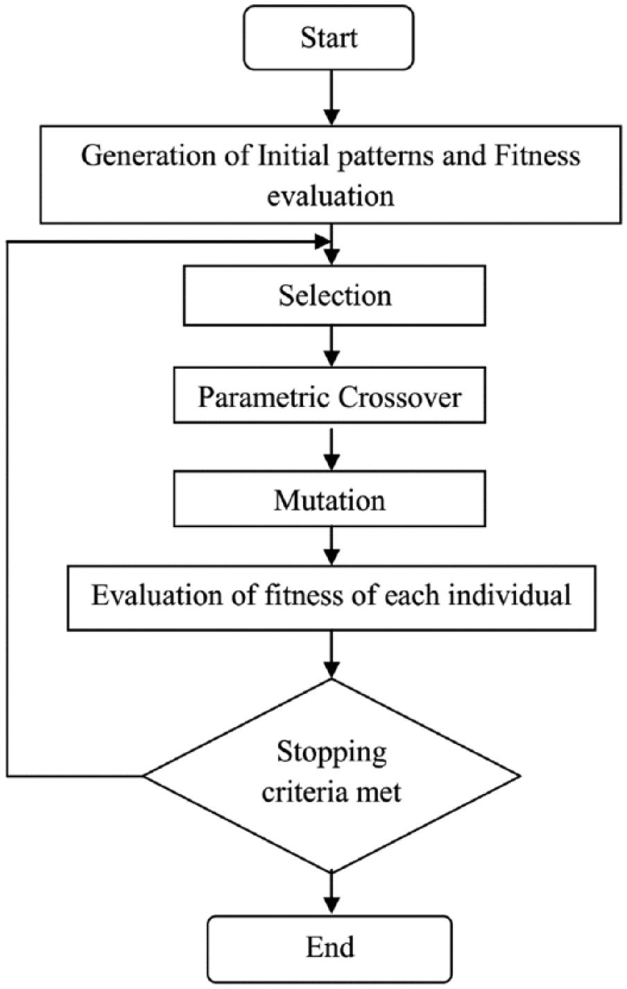
Flow diagram of GA-based thermal-aware test pattern generation.
Genotype
The genotype of a problem is the representation of an individual in the GA. For the experimentation, the test sets with don’t care bits generated using MinTest have been used. In this problem, the structure of the chromosome is x0, x1, x2, …, xn – 1, where n is the number of don’t care bits in one test pattern. Each x i can be either “0” or “1.” The don’t care bits in a test pattern are randomly filled using GA. A random number of chromosomes are produced to form the initial population. Two special vectors (all 0s and all 1s) that are corresponding to 0-fill and 1-fill are included in the initial population so that the result does not degrade below the value given all 0-fill and 1-fill algorithms.
Genetic operators
Genetic operators have been used in GAs to generate diversity and to combine existing solution. Direct copy, crossover and mutation have been used to evolve the new generations.
Crossover
Chromosomes from the population are selected as parents. The selection of parents involving in crossover has been biased toward the better fit chromosomes. A certain percentage (here 20%) of the population with minimum power density variance and minimum overall power (both static and dynamic) is considered to form the “best class.” 27 To carefully choose a chromosome for crossover, first a random number between 0 and 1 is generated. If the number is greater than 0.5, a chromosome from the best class is selected. Otherwise, a chromosome is chosen from the entire population. The procedure increases the probability of a better fit offspring getting selected. Similarly, the other parent gets selected.
After selecting two parent chromosomes, the new offspring are generated using the following procedure:
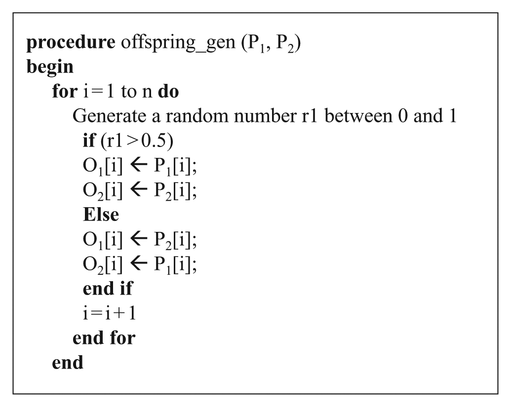
The newly generated offspring are checked for their uniqueness.
Mutation
Mutation is intended to maintain sufficient genetic diversity from one generation to the next. Mutation helped to prevent the algorithm from being trapped in a local minimum. First, two random numbers (r1 and r2) are generated between 1 and the width of the chromosome. The entries are toggled between the two positions. The resulting chromosome is modified to satisfy the uniqueness criteria. Here, we have taken the mutation rate as 10% of the total population.
Direct copy
The best chromosomes (possibly 20% of the total population) of every generation are copied to the next so that the possibility of degradation between the generations through a genetic operator is eliminated.
Termination
The GA process will terminate if there is no improvement in the best fitness of the population over that past 30 generations.
Fitness calculation
In order to carry out optimization using GA, a suitable fitness function has to be formulated to rank the chromosomes in a particular generation. In this work, the fitness function is formulated to reduce peak temperature and thermal variance as well as power consumption across the chip. The entire circuit is partitioned into a number of blocks. Each block contains flip-flops and several gates. In scan-based designs, test application is carried out by simultaneous scan-out current responses and scan-in of the next test pattern, and this process is repeated until all the test patterns are applied. During the scan-out and scan-in operations, many intermediate patterns are generated. These ripple patterns consume large power.
The objective of this work is to minimize the variance in power density between the blocks. In addition to that, the overall power consumption should be minimized. The variance S2 in power density for each test pattern t is defined as follows to analyze the spatial variation
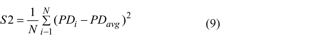

where N is the number of layout blocks for temperature analysis, PDi is the power density in block b i for each test pattern t, PDavg is the average power consumption among all the blocks for each test pattern t, Poverall is the total power consumption (dynamic and static power) for each test pattern t and MT-fill is the minimum transition fill for each test pattern t.
Results and discussion
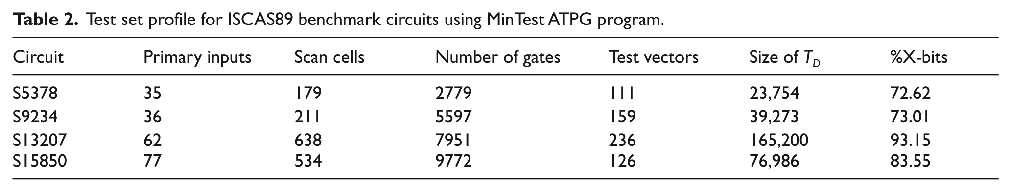
This section presents the results of experimentation with ISCAS89 benchmark circuits. The test sets generated using MinTest ATPG program have been utilized for the experiments. The characteristics of the MinTest test profile for ISCAS89 benchmarks are presented in Table 2.
Test set profile for ISCAS89 benchmark circuits using MinTest ATPG program.
Thermal simulation
Thermal simulation was used to estimate the power and temperature distribution across the block. The thermal simulation 28 steps are as follows:
Verilog circuit description is fed to the Synopsys Design Vision 29 to generate a gate-level netlist.
All normal flip-flops are converted into scan flip-flops using the Synopsys DFT Compiler. 30
IC Compiler 31 from Synopsys is used to create the floor plan of the scan inserted design using standard cell library. Scan netlist and the test patterns are used to estimate the power. The power consumption of each of the logic elements (gates and flip-flops) with different types and inputs is estimated using the Synopsys Design Vision tool and stored in a database. This database is used to convert the transitions in individual logic elements to their corresponding power values during circuit simulation for each scan shift and capture operation.
Synopsys IC Compiler is used to obtain floor plan information. The floor plan is divided into some blocks for thermal simulation. Power trace values are estimated for each of these blocks.
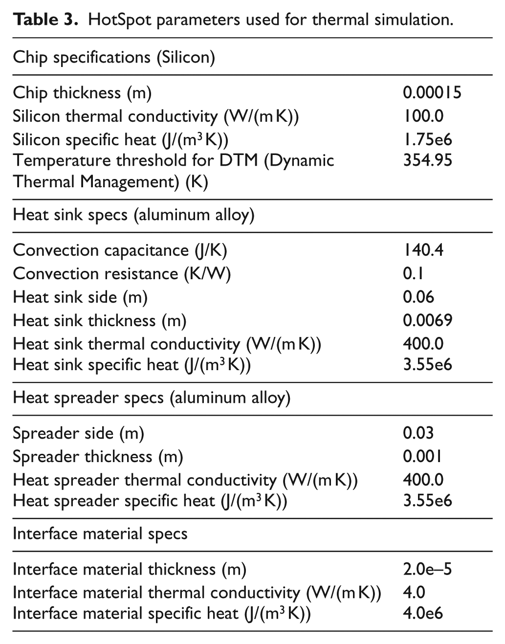
HotSpot, a thermal simulation tool, is used to perform thermal simulations. HotSpot takes power trace and block-level floor plan as inputs (Table 3).
HotSpot parameters used for thermal simulation.
Observation
Power consumption
Table 4 shows the percentage reduction in power variance, average power and peak power, respectively. ΔVpwr is the relative difference in power density variance, ΔPavg is the relative difference in the average power and ΔPpeak is the relative difference in peak power. The relative difference in power density variance is computed as
Percentage reduction in power variance, average power and peak power: comparison with other methods.
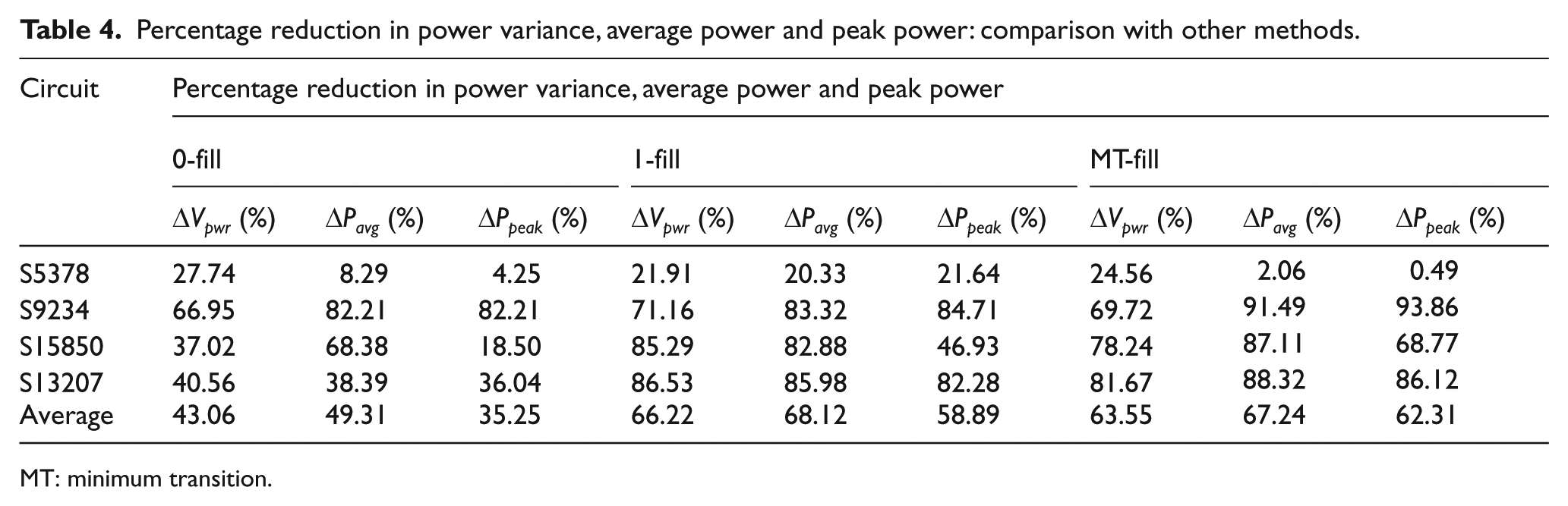
MT: minimum transition.
The results were obtained by an incompletely specified test set filled with known 0-fill, 1-fill and MT-fill and they were compared with the results of the proposed strategy. The results demonstrate that a significant reduction in spatial power density variance was obtained using the proposed X-filling method. In comparison with the various X-filling such as 0-fill, 1-fill and MT-fill, the proposed method achieved up to 43%, 66% and 64% reduction on average in power density variance, respectively. The proposed method also achieved up to 49%, 68% and 67% reduction on average in the average power when compared with 0-fill, 1-fill and MT-fill, respectively. The proposed method achieved up to 35%, 59% and 62% reduction on average in peak power when compared with 0-fill, 1-fill and MT-fill, respectively.
Yoneda et al. 22 achieved on average a reasonable reduction in power variance compared to low-power-oriented techniques such as 0-fill, 1-fill and MT-fill. They also mentioned that the method of Yoneda et al. 22 incurred around 35% increase in overall average power consumption. But our approach outperforms the low-power-oriented techniques by 49%–68% in average power consumption.
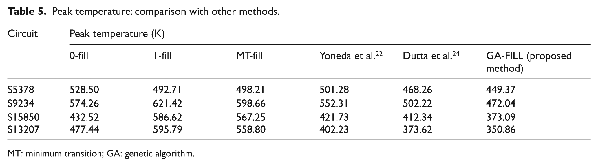
Temperature
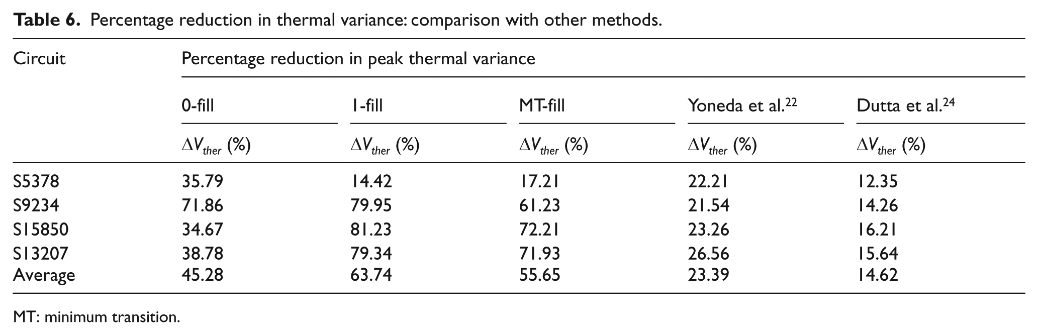
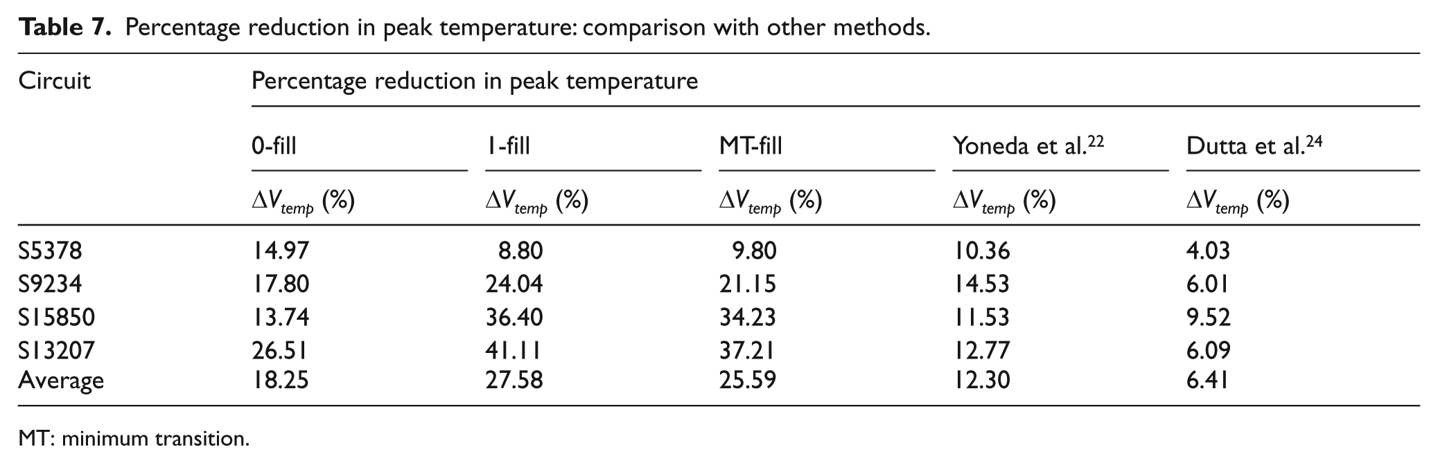
Table 5 shows the peak temperature values obtained by thermal simulation using HotSpot. Table 6 shows the corresponding percentage reduction in thermal variance. Table 7 shows the corresponding percentage reduction in temperature. ΔVtemp is the relative difference in peak temperature and ΔVther is the relative difference in thermal variance. The relative differences in peak temperature and in thermal variance are computed in a similar manner to ΔVpwr. The results demonstrate that a significant reduction in spatial thermal variance was obtained using the proposed X-filling method. In comparison with 0-fill, 1-fill and MT-fill, the proposed method achieved not only 45%, 64% and 56% reduction in thermal variance but also 18%, 28% and 26% reduction in peak temperature, respectively.
Peak temperature: comparison with other methods.
MT: minimum transition; GA: genetic algorithm.
Percentage reduction in thermal variance: comparison with other methods.
MT: minimum transition.
Percentage reduction in peak temperature: comparison with other methods.
MT: minimum transition.
In comparison with Dutta et al., 24 peak temperature has been reduced 4%–10% in our approach. In comparison with Yoneda et al., 22 peak temperature has been reduced 10%–15% in our approach. This is happening because the existing approach has considered only limited patterns. But the proposed method has considered reasonable patterns so that the peak temperature has been reduced.
The improvements obtained in the proposed case due to the power density variance among the blocks were minimized. The results also show that the peak temperature strongly depends on power distribution and the proposed method effectively minimizes the power density variance. So the peak temperature is minimized.
Conclusion
In this paper, a GA-based don’t care filling technique is proposed to deal with peak temperature minimization in deep submicron technologies. The main contribution of the algorithm is to fill the don’t care bits with a proper value (0 or 1) to reduce the spatial power density variance and temperature variance across the chip during manufacturing testing. The experimental results show that GA-based don’t care filling technique is more effective to minimize temperature and thermal variance while preserving the average power relatively at low level.
Footnotes
Declaration of conflicting interests
The author(s) declared no potential conflicts of interest with respect to the research, authorship and/or publication of this article.
Ethical approval
This article does not contain any studies with human participants or animals performed by any of the authors.
Funding
The author(s) received no financial support for the research, authorship and/or publication of this article.
Informed consent
Informed consent was obtained from all individual participants included in the study.