
Abstract
Microring resonators (MRRs) are the important devices for the development of silicon‐based optoelectronic integrated chips. Their composition of optical modules, such as optical modulators, switches, and optical logic gates, have greatly contributed to the development of the silicon‐based optoelectronics. However, due to the large radius of MRRs and the weak optical interaction of the silicon material itself, how to further improve integration and reduce power consumption is a great challenge. Combining graphene, which has many unique properties, with silicon‐based MRRs provides a good solution. Therefore, based on the interaction principle of graphene and light and the transmission principle of all‐pass silicon‐based MRRs, this article proposes for the first time a one‐bit optical numerical comparator based on MRRs, whose structure consists of four silicon‐based MRRs with a radius of 1.8 μm covering a single layer of graphene. The logic function of the one‐bit optical numerical comparator is realized by adjusting the different chemical potentials of the graphene. Simulation results shows that, with a TE mode light source at 1555.21 nm, the proposed optical numerical comparator obtains a minimum extinction ratio of 19.7 dB and a contrast ratio of 19.7 dB. Compared with the previously reported optical numerical comparators based on silicon‐based MRRs or ring resonators, the proposed optical numerical comparator has many advantages, such as high extinction ratio, high contrast ratio, compact structure, and high stability. It is beneficial to the development of silicon‐based photonic integrated devices.
1. Introduction
With the advantage of extremely low power consumption of photons, silicon‐based optoelectronics technology provides new solutions for the innovative development of a new generation of computers, optical communications, data centers, and other fields. Optical components such as microring resonators (MRRs) [1], III‐V semiconductor optical amplifiers (SOAs) [2], and Mach–Zendel interferometer (MZI) [3] are the key units that constitute the silicon‐based optoelectronic chips. Compared with SOA or MZI, silicon on insulator (SOI)–based MRRs have lots of advantages, such as small size, fast speed, easy tuning, low power consumptio, n and excellent resistance to electric fields [4]. In recent years, various logic gates (e.g., OR/NOR, AND/NAND, XOR/XNOR, and NOT gates), optical numerical comparators, temperature sensors, optical filters, multiplexers/demultiplexers, encoders/decoders, half‐add/full‐adders, and other integrated photonic devices have been designed using MRRs [5–10], which have greatly contributed to the development of optical combinational circuits and optical timing logic circuits. Among them, the optical numerical comparator is an important unit required for the implementation of all‐optical information processing devices. In recent years, by employing thermo‐optical or nonlinear effects of MRRs [11–14], many authors have designed optical numerical comparators with varying performance. However, the large radii of the microrings in the above devices, in the range of a few microns to tens of microns, lead to the difficulty of improving the integration of silicon‐based optoelectronic devices with MRRs. Moreover, this requires large power consumption to achieve resonant wavelength shifts due to the inherently weak optical interactions of silicon materials, making it challenging to achieve low power consumption and small size [15].
As one of the popular materials in silicon‐based optoelectronics, graphene has good electro‐optical properties, such as ultrahigh carrier mobility and ultrawide absorption bandwidth, which has been used in high‐speed graphene–silicon electro‐optical modulators [16, 17], optical switches [18, 19], saturable absorbers [20–22], photodetectors [23], and four‐wave mixing (FWM) [24, 25]. In particular, covering graphene on top of silicon‐based waveguides is an effective method to design and fabricate graphene–silicon hybrid modulation devices. When a bias voltage is applied to the graphene–silicon–based waveguide, carriers can accumulate on the patterned graphene structure, which conveniently modulates the Fermi energy level and thus enables light absorption [26]. To further improve the interaction between graphene materials and light, the combination of graphene and silicon‐based MRR to design graphene–silicon–based MRR electro‐optical modulators provides a good solution for implementing optical logic gates and optical logic computing circuits.
Therefore, based on the interaction principle between graphene material and light, this paper presents a graphene–silicon–based MRR‐based one‐bit optical numerical comparator for the first time, whose structure consists of four silicon‐based MRRs, a covering, a single layer of graphene, and a silicon‐based Y‐branch waveguide. The logic function of the one‐bit optical numerical comparator is realized by adjusting the different chemical potentials of the graphene. Simulation results show that the proposed optical numerical comparator obtains a minimum extinction ratio (ER) of 19.7 dB and a contrast ratio (CR) of 19.7 dB with the light source at 1555.21 nm. Compared with the previously reported optical numerical comparators based on silicon‐based MRRs, the proposed device has a higher ER, a more compact structure, better stability, and higher contrast, which is easy to integrate with other optical systems and is of great significance in optical computing circuits.
The rest of this paper is organized as follows. Section 2 introduces the modulation mechanism based on graphene‐silicon MRR. Section 3 introduces the proposed optical numerical comparator, Section 4 analyzes the simulation results, and finally the conclusion is given in Section 5.
2. Electro‐Optical Modulation Principle Based on Graphene–Silicon–Based MRR
Graphene is a two‐dimensional carbon nanomaterial in the shape of a honeycomb lattice [27], and its optical properties can be modeled by theoretical and experimental models such as the semiclassical model [28], the random phase approximation (RPA) [29], and the electron energy loss spectrum (EELS) [30]. By the semiclassical model, the simplified graphene conductivity can be obtained from the Kubo equation as follows [31]:
In the above equation, ω denotes the angular frequency, μ
c
denotes the chemical potential,τ denotes the relaxation time,ℏ denotes the approximate Planck constant, and e denotes the electron power. In addition, we can control the gate voltage of the graphene layer to change its chemical potential μ
c
, thereby changing its conductivity, as shown in the following equation [15]:
Among them, the Fermi velocity of graphene is v F = 106 m/s, and the externally applied voltage is V, and V D is the offset voltage generated by natural doping [15].
Therefore, the carrier interband jump of graphene is triggered by applying different bias voltages to the graphene to change its chemical potential. The overall process of optical jumping of graphene using applied bias voltage is shown in Figure 1.
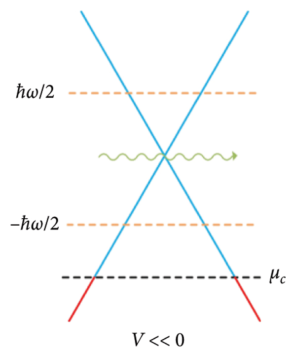
The process of applying bias voltage to graphene to produce optical jump: (a) no photon absorption, no interband jump. (b) Photon absorption, interband jump. (c) No photon absorption, no interband jump.
(b)

(c)

As shown in Figure 1(b), when the bias voltage is close to 0, due to the chemical potential of graphene (black dashed line) approaching the Dirac point (orange dashed line), electrons are allowed to transition from the electron‐occupied region (red line) to the unoccupied region (blue line), and the incident light is absorbed by graphene, resulting in photon absorption. Based on this principle, when the optical signal is incident on the MRR structure designed in this paper, graphene in a low chemical potential state absorbs more light, and the graphene silicon waveguide structure is in a high loss state, making the amplitude self‐coupling coefficient t equal to the ring transmission coefficient h. Then, MRR is in a critical coupling state, so the energy of the optical signal output from the through port is equal to 0. Similarly, as shown in Figures 1(a) and 1(c), when the bias voltage is much less than/greater than 0, the chemical potential of graphene (black dashed line) is less than/greater than half of the photon energy (ℏω/2). At this time, the MRR is in an under‐ or overcoupled state and does not produce photon absorption. Therefore, the energy of the optical signal output from the through port is much greater than 0 but less than the energy of the input light source.
In summary, by applying different bias voltages to graphene as the active part of the absorption modulator, the effective refractive index neff of the silicon‐based microring waveguide and the loss of optical signal transmission in the silicon‐based microring is changed so that the coupling state in the all‐pass silicon‐based MRR is switched between critical coupling and overcoupling, and thus the electro‐optical modulation function is realized.
3. Optical Numerical Comparator Based on Graphene–Silicon MRR
This study selected a silicon‐based MRR with a radius of 1.8 μm, which not only ensures that the modulator has a high output power but also has minimal impact on performance due to the low light absorption rate of graphene. Then, this article will elaborate in detail on the construction and parameters of the designed optical numerical comparator, and its specific layout can be seen in Figure 2(a).

Schematic structure of the optical numerical comparator based on graphene–silicon MRR: length L is 12 μm, width W is 10 μm, and height H is 0.4 μm. (a) Schematic diagram of the three‐dimensional structure. (b) Schematic diagram of the waveguide cross‐sectional structure. (c) Top view.
(b)

(c)
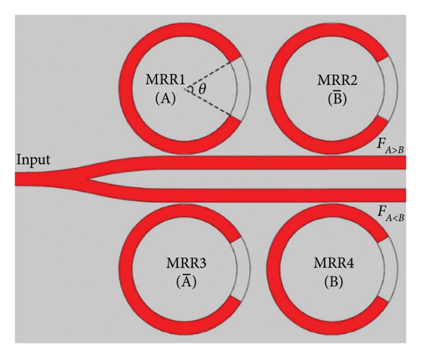
As shown in Figure 2(a), the optical numerical comparator mainly consists of four graphene‐covered silicon‐based MRRs, two silicon‐based straight waveguides, a Y‐shaped silicon‐based waveguide, and a SiO2 substrate. The structure of the device is symmetric about the X‐axis, with a coupling distance of 0.05 μm between the silicon‐based microring waveguides and the straight waveguides, and a circular distance of 4.5 μm between the two silicon‐based microring waveguides above the X‐axis. Figure 2(b) shows the cross‐sectional structure of the electro‐optical modulation region consisting of the silicon‐based waveguides, SiO2, hBN, and graphene. In this case, the silicon dioxide substrate is wrapped around the left side, right side, and bottom of the silicon waveguide, and metal sheets are used as electrodes and connected to the graphene and silicon waveguides, respectively.
On the top of the silicon‐based waveguide, the proposed structure is chosen to be covered with only one layer of graphene, with a 5‐nm‐thick layer of dielectric hBN separating the graphene from the silicon‐based waveguide, which not only prevents the carrier loaded into the graphene from being injected into the silicon‐based waveguide to affect the modulation effect but also enhances the interaction of the graphene with light, thus enhancing the effect on the effective refractive index of the silicon‐based waveguide. In addition, to prevent the performance of graphene from being affected by exposure to air, the top of graphene is covered with another 50 nm thick layer of SiO2.
Figure 2(c) shows the top view of the designed optical numerical comparator, where the states of MRR1 and MRR3 are controlled by the complementary binary logic level Signals A and When AB = 00, the corresponding When AB = 01, the corresponding


Similarly, the cases of AB = 10 and AB = 11 are similar to the above cases of AB = 01 and AB = 00, respectively. And the case of A > B or A < B is defined when the continuous optical signal operating at the wavelength of is only output from the FA>B port or FA<B port, and the case of A = B is defined when no optical signal is output from the FA>B port and FA<B port at the same time. In addition, θ is the coverage angle of graphene, and this angle determines the performance of the electro‐optical modulator based on graphene–silicon MRR. Therefore, the design of the optical numerical comparator requires the selection of a suitable θ value to obtain better performance, which is demonstrated in the next subsection.
4. Simulation Verification and Analysis
4.1. Building the Simulation Model
In order to test the effect of the coverage angle θ of graphene on the imaginary part and loss of the silicon‐based microring waveguide of neff, this paper first simulates the cross‐sectional structure of the waveguide in Figure 2(b) using MODE software from Lumerical and obtains the finite‐difference eigenmode (FDE) solver in MODE for the case of the incident light wavelength of 1.55 μm for the silicon‐based microring waveguide. The energy distribution of the optical field in the XZ plane is shown in Figure 3.
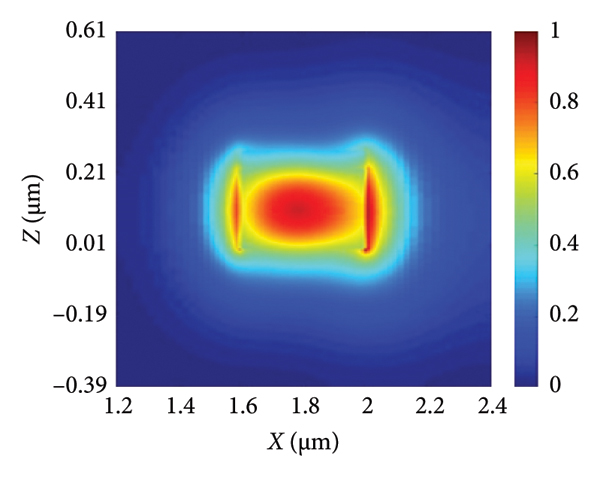
Mode optical field distribution in the XZ plane based on graphene–silicon based microring waveguide. (a) TE mode optical field distribution in the XZ plane at μ c = 0.5 eV. (b) TM mode optical field distribution in the XZ plane at μ c = 0.5 eV.
(b)

By comparing Figures 3(a) and 3(b), it can be found that the light field energy of TE mode can be bound to the center of the silicon‐based microring waveguide compared to the dispersion distribution of the light field energy of the TM mode, and a part of the light field energy is dissipated to the right side of the waveguide (the outer side of the microring waveguide) due to the bending loss. Therefore, the TE mode light source is chosen for the subsequent experiments in this paper.
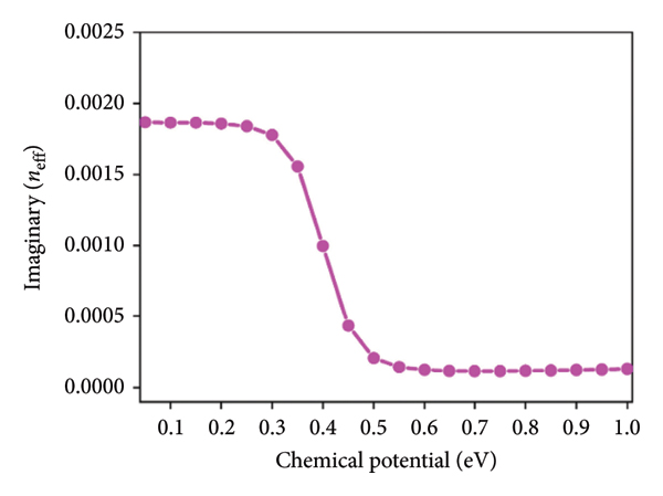
Then, based on the above results, this paper proceeds to analyze the neff parameters and loss parameters of the silicon‐based microring waveguide with different chemical potentials through the FDE solver simulation and obtains the neff curves and loss curves with the change of chemical potential, as shown in Figures 4 and 5, respectively. It can be seen from Figure 4(a) that with the changing chemical potential of graphene, although the real part of the neff curve of the silicon‐based microring waveguide undergoes significant fluctuations, the maximum change caused is only 0.0033. Thus, it can be seen that the single‐layer graphene has little effect on the real part of the silicon‐based microring waveguide. The imaginary part of the neff of the Si‐based microring waveguide changes dramatically from 0.0019 to 1.24e − 4 as the chemical potential of graphene changes from 0.2 to 0.6 eV, a difference of about 15 times, which clearly shows the important influence of graphene on the imaginary part of the Si‐based microring waveguide. The imaginary part of neff represents the loss generated by the transmission of the optical signal in the silicon‐based microring waveguide, and its trend determines the trend of the loss, which can be seen from the graph of loss versus chemical potential in Figure 5.

Effective refractive index plotted against chemical potential. (a) Plot of the real part of neff versus chemical potential. (b) Plot of the imaginary part of neff versus chemical potential.
(b)
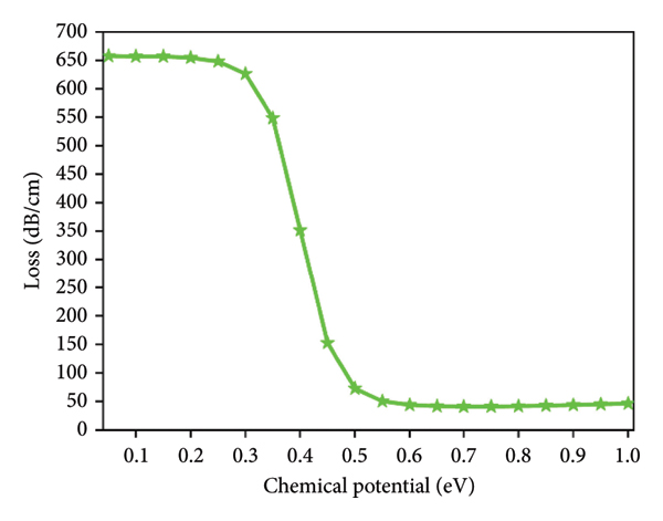
Plot of loss with chemical potential.
The variation curves of the imaginary part of neff and the variation curves of the loss prove the absorption of the optical signal energy in the silicon‐based waveguide by graphene, but further observation of Figures 4(b) and 5 reveals that the chemical potential of graphene has the best effect on the silicon‐based microring waveguide at 0.05 and 0.7 eV, respectively, showing the maximum or minimum absorption effect of graphene on the optical signal. Therefore, the chemical potential of 0.7 eV is chosen as the “on” state and the chemical potential of 0.05 eV is chosen as the “off” state of the graphene–silicon–based MRR modulator.
The effective refractive index, loss, propagation constant, group refractive index, and dispersion of the optical waveguide in the wavelength range of 1.5∼1.6 μm were obtained by the frequency scan function of the FDE solver. Meanwhile, the coupling coefficient versus wavelength curves between the microring waveguide and the straight waveguide at a fixed coupling spacing were obtained by the FDTD software, as shown in Figure 6. Among them, the coupling coefficient is affected with the increase of graphene coverage angle θ. Then, all the above related parameters are imported into Lumerical’s INTERCONNECT (photonic integrated circuit software) for simulation and analysis.
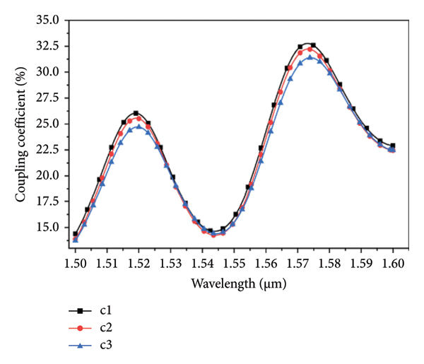
Plot of coupling coefficient versus wavelength: c1 represents graphene away from the coupling region; c2 represents the coupling region containing a single layer of graphene with a chemical potential of 0.7 eV; c3 represents the coupling region containing a single layer of graphene with a chemical potential of 0.05 eV.
4.2. Model Parameter Optimization
For the effect of the coverage angle θ of graphene on the performance of the proposed optical numerical comparator, a photonic integrated circuit based on a graphene‐single silicon‐based MRR modulator is built in INTERCONNECT, as shown in Figure 7. In Figure 7, the parameter settings of input straight waveguide, output straight waveguide, uncovered graphene microloop waveguide, covered graphene microloop waveguide, and coupler are obtained from the simulation in MODE or FDTD, and the remaining parameter settings are shown in Table 1. Except for the relevant parameter settings listed in Table 1, the default settings of INTERCONNECT software are used for all other parameters required for each device.
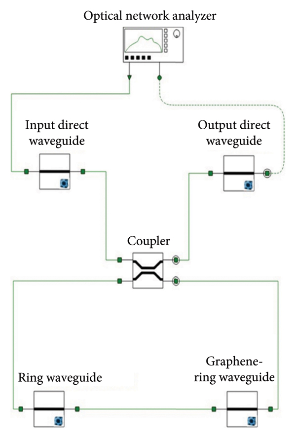
Simulation structure of the graphene‐single silicon‐based MRR‐based modulator.
Simulation parameter settings for the graphene‐single silicon‐based MRR‐based modulator.
In the INTERCONNECT software, the change in the coverage area of graphene was simulated by changing the magnitude of θ. The curve of the normalized power of the modulator output with θ is shown in Figure 8.

Curves of the normalized power at the output of the modulator with respect to θ. (a) Normalized power curve with θ at a chemical potential of 0.05 eV. (b) Normalized power curve with θ at a chemical potential of 0.7 eV.
(b)
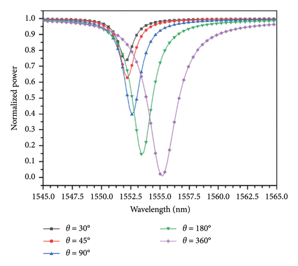
It can be seen from Figure 8 that the normalized power output of the modulator gradually decreases with the gradual increase of the graphene coverage angle θ, both in the case of chemical potential 0.05 eV and in the case of chemical potential 0.7 eV. By comparing the normalized power curves in Figures 8(a) and 8(b), regardless of the magnitude of θ, the normalized power output by the modulator acquires the lowest power at a chemical potential of 0.05 eV, while its normalized power at a chemical potential of 0.7 eV is also lower. Therefore, in order to further judge the effect of the magnitude of θ on the modulator performance, the ER and CR were introduced to calculate the modulator output port performance, and the curve of ER with θ was made in Figure 9.
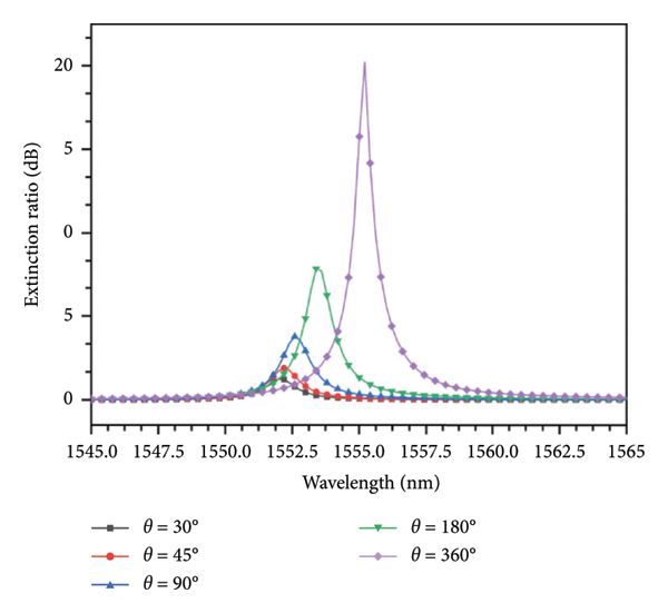
Extinction ratio curve with θ.
In Figure 9, compared with other θ values, the fluctuation of the ER curve with wavelength at the output port of the modulator is very obvious when the graphene coverage angle θ = 360°, and the maximum ER is achieved at the incident light wavelength of 1555.21 nm, which indicates that the optical signal at the wavelength of 1555.21 nm is transmitted in the silicon‐based microring to reach the optimal switching between critical coupling and overcoupling, when the modulator performance reaches the optimum. Therefore, this paper determines that the coverage angle of single‐layer graphene on the silicon‐based microring waveguide is 360°, and the single‐layer graphene completely covers the top of the silicon‐based microring waveguide. Then, according to the above simulation method and idea, the simulation structure of the proposed graphene‐silicon‐based MRR based optical numerical comparator in INTERCONNECT software in this paper is shown in Figure 10, and the simulation‐related parameter settings are shown in Table 2. Except for the parameter settings in the table, the parameters of the remaining devices in the figure are the same as those of the simulation of the graphene‐single silicon‐based MRR‐based modulator.

Simulation structure of the graphene–silicon MRR‐based optical numerical comparator in INTERCONNECT.
Simulation parameter settings for the graphene–silicon–based MRR with optical numerical comparator.
4.3. Optical Performance Indicators of MRR
Among them, ER [32] is the criterion for judging the transmission performance of the optical device, and the larger its value, the more stable and high resolution the transmission of the all‐optical device is; CR [33] represents the difference between the actual output high power and low power in the optical device, and the larger its value, the better.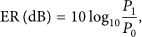
Among them, P1 is the output power of logic state “1”, P0 is the output power of logic state “0”, 


4.4. Simulation Results and Analysis
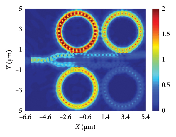
Figures 11(a), 11(b), 11(c), and 11(d) depict the simulation outputs for the AB = 00, AB = 01, AB = 10, and AB = 11 combinations, respectively. While the proposed optical numerical comparator is simulated using the INTERCONNECT software, the simulation is also performed in this paper using the 3D FDTD software, and Figures 12(a), 12(b), 12(c), and 12(d) show the electric field distribution of four states on the XOY plane.
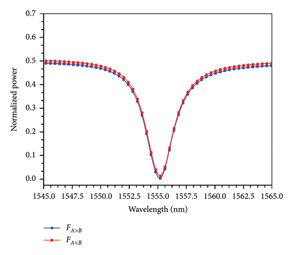
Normalized power of each output port for each combination case. (a) AB = 00. (b) AB = 01. (c) AB = 10. (d) AB = 11.
(b)

(c)

(d)

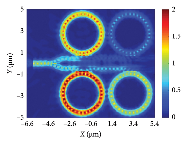
The electric field distribution of four states on the XOY plane. (a) AB = 00. (b) AB = 01. (c) AB = 10. (d) AB = 11.
(b)
(c)
(d)
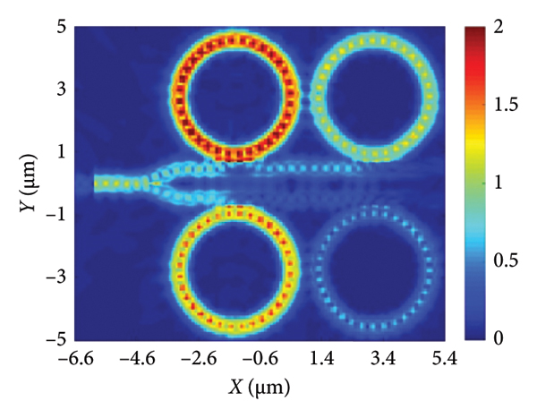
From Figures 11(a) and 11(d), it can be seen that the normalized power output from FA>B port or FA<B port is almost coincident at 1555.21 nm wavelength when AB = 00 or AB = 11. And in Figures 11(b) and 11(c), when AB = 01 or AB = 10, the normalized power output from FA>B port and FA<B port has a clear contrast at 1555.21‐nm wavelength.
In Figure 12(a), the optical signal passes through the Y‐branch waveguide and enters the upper and lower branches for transmission. Under the control of AB = 00 and 
Comparison of the logical values of the proposed one‐bit optical numerical comparator with the simulation results.
Then, according to Equations (3) and (4), the minimum ER of the proposed one‐bit optical value comparator is 19.7 dB for both FA>B port and FA<B port, and the CR is also 19.7 dB. The proposed optical value comparator is compared with some one‐bit optical value comparators proposed in recent years, as shown in Table 4.
Comparison of the proposed one‐bit optical numerical comparator with the one‐bit optical numerical comparator reported in recent years.
Note: Some references in the table do not give the actual area, so the area is estimated based on the microring radius and labeled as “approximate”.
asimulation experiment.
bproduction preparation.
According to Table 4, it can be seen that in terms of area, although the device area is larger than the structure proposed in [13], it is smaller than the structures proposed in other literature, and the minimum ER obtained is much higher than the maximum or minimum ER of other optical numerical comparators. The larger the ER, the more obvious the difference in optical power, and the better the robustness. Therefore, it proves that the designed optical numerical comparator has high stability. In terms of contrast, due to the symmetrical structure of the proposed optical numerical comparator, the output results of FA>B port and FA<B port are symmetrical. This makes the contrast value equal to the minimum ER, and its contrast is much greater than other optical numerical comparators, indicating that the on/off difference range of the device is larger and more discriminative.
5. Conclusion
In summary, this paper proposed a one‐bit optical numerical comparator based on graphene–silicon MRR using the principle of light absorption by graphene, which consists of four silicon‐based MRRs with a radius of 1.8 μm and an area of 120 μm2. By controlling the chemical potential of the graphene with an applied bias voltage, the effective refractive index of the silicon‐based microring waveguide and the loss of optical signal transmission are changed so that the coupling state in the all‐pass silicon‐based MRR switches between critical coupling and overcoupling. In this paper, the proposed one‐bit optical numerical comparator is simulated using Lumerical’s MODE, FDTD, and INTERCONNECT software, and the results show that the proposed optical numerical comparator achieves a minimum ER of 19.7 dB and a CR of 19.7 dB under the TE mode light source of 1555.21 nm. Compared with previously reported optical numerical comparators based on silicon‐based MRRs or ring resonators, the proposed optical numerical comparator has the advantages of high ER, high CR, and compact structure.
Data Availability Statement
The data used in this article are confidential.
Conflicts of Interest
The authors declare no conflicts of interest.
Funding
This work was supported in part by the National Natural Science Foundation of China (62461011), Guangxi Natural Science Foundation (2025GXNSFAA069299), 2022 Shanxi Provincial Major Science and Technology Special Project (202201030201009), Guangxi Key Laboratory of Brain‐Inspired Computing and Intelligent Chips (BCIC‐24‐K1), and Guangxi Key Laboratory of Automatic Detecting Technology and Instruments (YQ22110).