
Abstract
The effect of spark voltage on nanoparticle (NP) formation, crystal structure, and optical properties of Zn and Ag‐containing metal oxides produced using the spark‐discharge (SD) technique was investigated. Quasispherical‐shaped nanocrystals were observed in ZnO, Ag:ZnO, and AgO NP samples prepared at different spark voltages. The NP sizes in ZnO and Ag:ZnO samples were close and decreased as the spark voltage increased. It was observed that when AgO was prepared with only low‐spark voltage (4.3 kV), tetrahedron/octahedron‐shaped NPs were also formed. 4.3 kV spark voltage increased the crystal growth rate in the (100)‐plane and 7 kV spark voltage also increased the crystal growth in the (002)‐plane in hexagonal wurtzite ZnO and Ag:ZnO samples. Therefore, the a‐axial preferred orientation of these samples at low‐spark voltage had switched to the c‐axial preferred orientation at high‐spark voltage. For AgO, the increase in spark voltage revealed the monoclinic structure more strongly. The film thicknesses of AgO samples were close to each other with both spark voltages. Although, it was determined that the AgO prepared with 7 kV was optically more transparent and its optical band gap was significantly widened. This case may be due to the more presence of dodecahedral‐shaped particles in the morphology of the AgO sample prepared. Therefore, the wider optical band gap of metal oxides decorated with such nanoparticles could indicate facet dependency. In addition, the film thickness and optical band gap of both ZnO and Ag:ZnO samples increased significantly depending on the increase of spark voltage. The optical band gap narrowed (redshifted) due to the effect of Ag ions entering the ZnO structure. As the spark voltage increased, the difference between the optical band gaps of ZnO and Ag:ZnO also increased. With the spark‐voltage effect, the change in preferential crystallographic orientations of ZnO and Ag:ZnO samples and the change in optical band gap depending on the NP shape of the AgO sample can offer significant advantages in terms of optoelectronics.
1. Introduction
Nanoparticles (NPs), ranging in size from 1 nm to 100 nm, exhibit unique physical and chemical properties compared to their bulk forms. In addition to metal nanoparticles, oxide forms, particularly semiconductor metal oxides, find application in various technological areas such as active gas‐sensing materials [1–8]. On the other hand, nanoparticles are highly significant due to their size similarity to many biological substances, offering potential solutions to health problems [9–11]. Several studies demonstrate that the physical properties of metal oxide nanoparticles doped with metal atoms are adjustable [12–15]. The sizes and shapes of these nanoparticles can significantly influence their physical properties, with deposition methods playing a crucial role. For example, silver nanoparticles can take various shapes such as spherical, nanorods, nanowires, cubic, and triangular forms synthesized through chemical reduction methods using different chemical reductants.
In addition to the physical, chemical, and biological synthesis methods used to produce nanoparticles, the spark‐discharge (SD) technique has been proven to prepare nanoparticles in metal oxide form. The SD technique is one of the simplest techniques among the other physical methods such as evaporation‐condensation, laser ablation, electrical irradiation, gamma irradiation, and lithography. This technique, which was first used by Schwyn et al. in 1988 [16], is a compact and versatile method to produce nanoparticles (NPs) from different types of materials. In addition, the synthesis can be performed at atmospheric pressure which is quite economical in comparison with vacuum methods and has the potential of being scaled up. In this method, NPs with different geometries can be formed considering the amount of energy stored in the capacitor, the melting temperatures of the electrode materials, the work functions, electron affinities, and oxygen environment for the formation of oxide forms and substrate types. The adhesion of nanoparticles to the surface results from interactions between the surface and nanoparticles. The free energy of the substrate may be a factor affecting the adhesion of nanoparticles to the surface. Subsequently, a large number of research groups produced nanoforms of carbon [17], carbon flakes [18], metals [19], metal oxide NPs [20, 21], and semiconductor Si NPs [22]. This method was also used for depositing ZnO NPs and co‐doped ZnO NPs and Cu‐doped ZnO NPs using high‐purity Zn, Co, and Cu metal wires in our previous studies [23, 24]. Among these oxides, Zn oxide NPs (ZnO) are of special interest, because doping of metals into ZnO can change the band gap, the crystallite size, and other properties such as magnetic properties. In order to use optoelectronic devices as front electrodes, materials with high conductivity and high transparency need to be developed. Among metal oxides with wide bandgap, doped zinc oxide (ZnO) is very promising for use as a transparent electrode. Apart from solution‐based techniques, oxygen vacancies created by the addition of Ag and Al act as defect centers in ZnO materials, especially in thin film forms consisting of nanoparticles. In fact, higher electrical conductivity was observed in both Ag and Al and Ag codoped ZnO materials compared to carbon nanotube‐based transparent electrodes [25]. In addition, different forms of Ag‐Zn compounds prepared by anodic oxidation can be used in different technological applications. For example, Ag/ZnO nanorods are effective catalysts and photocatalysts; the nanowire form can be used as a photodetector, and the nanolayer form is a metal‐semiconductor junction [26]. In particular, the interaction of Ag nanoparticles with various substrates and their technological uses has been investigated [27–30]. In addition, there is a theoretical study suggesting that transition metal oxides can provide a solution to the problems encountered in fuel cells with their oxygen‐reduction properties [31]. With the new features added to this technique, the effects of electric field and magnetic field on the formation of metal oxides are also examined. For example, an external electric field is used to increase both the uniformity and deposition rate of TiO2 films during the spark‐discharging processes [32]. The SD technique under a magnetic field was used to investigate the effect of magnetic metals such as Fe, Ni, and Co on the electrochromic properties of WO3 [33]. In addition, the influence of the magnetic field on the chemical reaction of nitrogen and carbon dioxide in sparking the electric discharge of zinc wires was examined [34].
It is important to control the crystallographic orientation of the metal oxides because metal oxide nucleations on the substrate surface have a certain crystal growth direction depending on certain deposition conditions. Both crystal structure types and their planes can determine many properties of a material and this case can increase the diversity in the technological applications. Moreover, the factors causing the change of crystallographic orientation or the crystal growth rate can improve other properties such as optical, electrical, mechanical, magnetic, and biomedical of that material. In this study, we aimed to investigate the effects of spark voltage on the formation of NPs with various shapes and sizes, their crystallographic preferential orientations, crystal structure, and optical constants in Zn and Ag‐containing metal oxide NP thin film samples prepared with the SD technique. The accumulation and agglomeration of nanoparticles on the substrate surface directly depend on the stored electrostatic energy [35]. At smaller spark voltages, the distance between electrodes also needs to be reduced. In this case, the effective cross‐sectional area of the scattered nanoparticles may be very small and may also cause accumulation in a single center. With increasing high‐voltage values, the distance between electrodes also increases. For example, considering the dielectric coefficient of air under normal atmospheric conditions, about 30 kV/cm is the threshold value for discharge. As the discharge voltage increases, the stored electrostatic energy value also increases. In this case, it becomes very difficult for more energetic nanoparticles to accumulate in a homogeneous distribution around a center during discharge. For this reason, two medium‐sized spark voltages such as 4.3 kV and 7 kV were selected in this study. Scanning electron microscopy (SEM) and X‐ray diffraction (XRD) measurements for structural properties and UV‐Vis optical transmission measurements for optical properties of the samples deposited on the substrate were carried out, and the results were examined. The Kelvin (4‐wire) method is used for the electrical characterization of samples under normal atmospheric conditions.
2. Materials and Methods
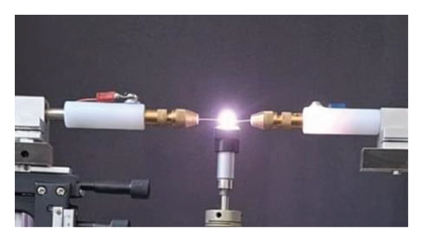
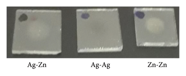
The spark‐discharge system used in this study basically consists of a high‐voltage source, a capacitor for storing electrostatic energy, and an electromechanical unit for adjusting the distance between the electrodes and the substrate (Figure 1(a)). There are some studies in which nanoparticles are prepared using source metals such as Zn, Cu, and Co with different geometries, such as horizontal or vertical, and with modified SD systems [23, 24, 36]. High‐purity zinc and silver wires such as metal electrodes were used as the source materials. Zn‐Zn, Ag‐Zn, and Ag‐Ag electrode pairs were used for Zn‐based oxide, (Ag, Zn)‐based bimetallic oxide, and Ag‐based oxide NP thin film samples, respectively. The microscope glasses were used as the substrate, which was sonically cleaned in distilled water, ethanol, and acetone and then dried. The distance between the electrodes and substrate was controlled manually with the help of micrometers (Z‐stage). In the horizontal geometry, the anode and cathode were placed horizontally at 2 mm above the substrate. The substrate was moved circularly during the deposition to ensure a homogeneous distribution of nanoparticles in the SD system. Here, the rotation speed of the substrate was controlled by a microcontroller (Arduino Uno) and a stepper motor driver unit. The distance between the electrodes was controlled manually with the help of two micrometers, trying to keep it constant during the deposition of the nanoparticles. To protect the high‐voltage source from back current, a high‐voltage diode was inserted between the source unit and capacitor. A high‐voltage probe connected to a multimeter was used to monitor the voltage across the capacitor to discharge. The abrasion at the ends of the electrodes occurred during the discharge of the stored electrical potential energy between the electrodes. Photographs of metal electrodes (Zn and Ag) before (label B) and after (label A) the spark‐discharge process for the SD system are given in Figure 1(b). The sparking occurred when the 0.2 µF capacitor charged with 4.3 kV (1.85 J, low energy) and 7 kV (4.9 J, high energy) voltages was discharged with a rotary switch. The photograph of the spark moment occurring between the electrodes is shown in Figure 1(c). This process was performed repeatedly 200 times with a sparking time of 3 s/spark at atmospheric pressure in ambient air. Photographs of the samples were obtained by using Ag–Zn, Ag‐Ag, and Zn‐Zn for 4.3 kV discharge voltage (Figure 1(d)).

(a) Schematic diagram of the spark‐discharge system, (b) photographs of metal electrodes (Zn and Ag) before (B) and after (A) the spark‐discharge process, (c) photograph of the spark‐discharge moment, and (d) photographs of metal oxide NP thin films obtained by using Ag–Zn, Ag‐Ag, and Zn‐Zn electrode pairs.
(b)

(c)
(d)
The crystal structure was investigated by X‐ray diffraction (Rigaku Ultima‐IV) using CuK α1 radiation (λ = 1.5406 Å). Compositional and morphological information of the samples has been gained using a scanning electron microscope (SEM, FEI Quanta FEG 250) equipped with energy‐dispersive X‐ray analysis (EDX). The optical transmittance measurements of the samples were carried out at room temperature using a T60 model spectrophotometer (PG Instruments) in the wavelength range of 300–900 nm. For the optical transmittance measurements, a special mask with a 2 mm diameter was centered on the spark‐affected region of the samples. The resistivity of thin films was determined by a 4‐wire method using a Keithley 2400 model source‐measure unit. By using a computer program developed using LabVIEW software, source meter was connected to the computer. The Kelvin clips were used for injection of current and corresponding voltage measurement.
3. Results and Discussion
3.1. Structural Properties
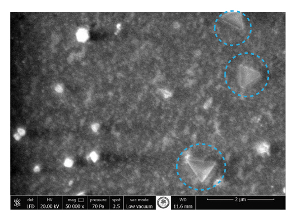
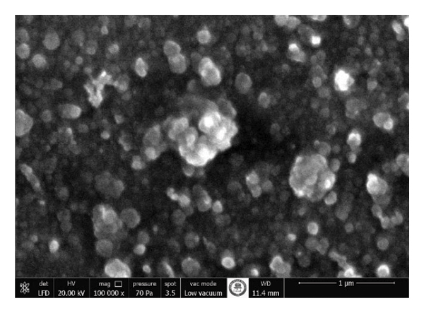
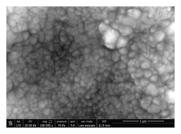
The SEM analysis was performed at high magnification at the center of all spark‐induced metal oxide NP thin films. The SEM images of the samples deposited using Ag‐Ag, Ag‐Zn, and Zn‐Zn electrodes under 4.3 kV and 7 kV discharge voltages are indicated in Figures 2(a), 2(b), 2(c), 3(a), 3(b), and 3(c), respectively. Among the particles examined, it was found that the spark‐discharge voltage and the electrostatic energy stored in the capacitor affect both the size and shape of the metal oxide nanoparticles. Formations with hexagonal surfaces with smooth corners can be seen as circular in 2‐dimensions and spherical in 3‐dimensions (inside the red dashed circle); thus, quasispherical expressions have been used for the shape of this form (Table 1). Formations with a pyramidal appearance, where the triangle corners of particles that appear triangular in 2‐dimensional (inside the blue dashed circle) meet, also point to different 3‐dimensional formations close to this form.
SEM pictures for metal oxide NP thin films by using (a) Ag‐Ag, (b) Ag‐Zn, and (c) Zn‐Zn electrode pairs under 4.3 kV spark‐discharge voltage, and (d) possible polyhedral shapes for the Ag‐based oxide nanocrystal formations.
(b)

(c)

(d)


SEM pictures for metal oxide NP thin films by using (a) Ag‐Ag, (b) Ag‐Zn, and (c) Zn‐Zn electrode pairs under 7 kV spark‐discharge voltage.
(b)
(c)
For different spark‐discharge voltage V S , the atomic weight percentage of zinc, oxygen, and silver ions, sizes, and shapes of NPs in metal oxide samples obtained from EDX measurements.
7 kV spark discharge provides the mixed formation of quasispherical nanoparticles with an average diameter value of 317 nm and cube‐shaped NPs with an average side length of 130 nm when the Ag‐Ag electrodes were used to obtain Ag‐based oxide NP sample (Figure 3(a)). However, in the Ag‐based oxide NP sample under 4.3 kV spark‐discharge voltage, triangular‐shaped NPs with an average side length of 670 nm, cube‐shaped NPs with a side length of 220 nm, and quasispherical NPs with a diameter of 95 nm were observed (Figure 2(a)). It has been known that the quasispherical formations present in the SEM images of Ag‐based oxides may arise from nanocrystals in different polyhedral shapes [37–39]. Similarly, in this study, it can be said that the triangular, spherical‐hexagonal, and cubic‐shaped particles found in the SEM images of Ag‐based oxide samples prepared with 4.3 kV spark voltage were actually nanocrystal formations of Ag‐oxide phases in different shapes. Structures similar to the polyhedral shapes given in Figure 2(d) were observed in all Ag‐based oxide samples. For the sample obtained with Ag‐Ag electrodes under 4.3 kV spark voltage, it was clearly observed that the triangular structures were actually in tetrahedron or octahedron 3‐dimensional forms (Figure 2(a)). In the Ag‐based oxide NP sample produced under higher spark voltage, it was seen that tetrahedral (or octahedral) particles disappeared, but quasispherical (spherical‐hexagonal) and cubic particles were present. It is possible that the structures mentioned as quasispherical in the SEM images here were 3‐dimensional structures such as octahedrons, dodecahedrons, and icosahedrons as shown in Figure 2(d). In addition, in the Ag‐based oxide sample prepared under 7 kV, an increase in the size of quasispherical forms and a decrease in the size of cubic forms were detected. Nanocrystal formations of Ag‐based oxide phases will appear more clearly depending on the spark voltage, spark number, oxygen environment, and substrate type that will support the amount of metal or oxygen in the formation of the phases. Substrate type is also an important factor in the adsorption energy of nanoparticles.
When the Ag‐Zn electrodes were used, it was observed that the average size of obtained quasispherical (Ag, Zn)‐based oxide NPs was 130 nm under 7 kV spark voltage (Figure 3(b)). When the spark voltage decreased up to 4.3 kV, the average size of these nanoparticles was found as 57 nm ± 16 nm (Figure 4). In both cases, (Ag, Zn)‐based oxide NPs were distributed very smoothly and homogeneously on the substrate. The average size of the Zn‐based oxide quasispherical NPs under 7 kV spark voltage was found to be 180 nm. The average size of Zn‐based oxide NPs was found as 66 nm ± 20 nm under 4.3 kV spark voltage. The size distribution of these nanoparticles obtained by using Zn‐Zn electrodes is shown in Figure 5.

(Ag, Zn)‐based oxide NP diameter distribution histogram for 4.3 kV spark voltage.
(b)


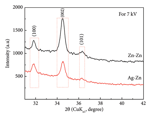
For 7 kV spark‐discharge voltage, XRD patterns of the samples by using (a) Zn‐Zn and Ag‐Zn electrode pairs according to reference for ZnO (JCPDS no. 36–1451) and (b) the intensity and Bragg angle differences of (100), (002), and (101) peaks for the samples.
(b)
The XRD pattern of the Zn‐based oxide NP sample deposited with 4.3 kV spark voltage includes the diffraction peaks with their corresponding hkl values determined as 31.850° (100), 34.492° (002), 36.426° (101), 56.325° (110), and 66.342° (200). These diffraction peaks have matched with the main peaks of the hexagonal wurtzite structure of ZnO defined by JCPDS (no. 36–1451). It was observed that the XRD pattern of (Ag, Zn)‐based bimetallic oxide NP sample deposited with 4.3 kV spark voltage includes the diffraction peaks with their corresponding hkl values determined as 31.846° (100), 34.320° (002), and 47.756° (102). The crystal structure of the (Ag, Zn)‐based bimetallic oxide NP sample deposited with 4.3 kV spark voltage also matched very well with the ZnO hexagonal wurtzite structure. Since the dominant peak in both Zn‐based and (Ag, Zn)‐based oxide NP sample came from the (100)‐plane, it was seen that the crystal orientation was in the a‐axis direction. In addition, the introduction of Ag ions into the ZnO structure reduced the intensity of the (100) peak by 92%, the (002) peak by 85% (Figure 6(b)), and the (200) peak by 85%. Ag doping shifted the position of the (100) peak slightly to the left by 0.02%, that of the (002) peak by 0.5% to the left, and that of the (200) peak by 0.2% to the right.
Figure 7(a) shows the XRD patterns of Zn‐based and (Ag, Zn)‐based oxide NP samples deposited under 7 kV spark voltage. The Zn‐based oxide NP sample deposited under 7 kV spark voltage has the main peaks of the hexagonal wurtzite structure of ZnO, whose crystal structure is also defined by JCPDS no. 36–1451. The main diffraction peaks of the Zn‐based oxide NP sample were observed as 31.834° (100), 34.503° (002), 36.329° (101), 47.377° (102), 62.928° (103), and 66.416° (200). Since the dominant peak in the XRD pattern of the sample was from the (002) plane, it was seen that there was a preferentially oriented crystal structure in the c‐axis. The main diffraction peaks of (Ag, Zn)‐based oxide NP sample deposited with 7 kV were observed as 31.814° (100), 34.529° (002), 36.301° (101), 47.761° (102), and 63.053° (103). The crystal structure of the (Ag, Zn)‐based bimetallic oxide NP sample deposited with 7 kV spark voltage also matched the ZnO hexagonal wurtzite structure very well. The preferential crystal orientation of this sample was also along (002), that was, on the c‐axis. In this study, for Zn‐based oxide NP samples having hexagonal wurtzite structures, differences in the preferential orientations occurred according to the higher crystal growth rates depending on spark voltage in the (100) and (002) planes [42]. Compared to the Zn‐based oxide sample, it was observed that the intensity of the (002) peak of the (Ag, Zn)‐based bimetallic oxide sample decreased by 55% and the Bragg angle shifted slightly to the right (0.1%). Ag doping caused a 14% decrease in (100) peak intensity and a 49% decrease in (101) peak intensity (Figure 7(b)). The (100) peak position shifted slightly to the right by 0.02%, and the (101) peak position shifted slightly to the left by 0.1%. Higher spark voltage (7 kV) increased the (002) peak intensity of the Zn‐based oxide NP sample considerably and shifted it to the right by 0.15%. In addition, the (100) peak intensity was reduced considerably and shifted slightly to the left. In the (Ag, Zn)‐based bimetallic oxide NP sample, the higher spark voltage caused the increase of the (100) peak intensity by 12% and (002) peak intensity by 94%. It was observed that both peak positions shifted slightly (1%) to the left. It was observed that spark voltage value affects the crystallographic planes in the hexagonal wurtzite structure of Zn‐based and (Ag, Zn)‐based oxide NPs. Ag‐doped ZnO NP thin films were prepared with pure Zn and Ag wires. The effect of Ag ions on the ZnO crystal structure in nanostructures prepared with the effect of a certain spark voltage can be determined by shifts in Bragg angles in XRD patterns. The amount of shift in peak positions may vary depending on the amount of Ag in the host structure. When the spark voltage increased, the a‐lattice parameters of Zn‐based and (Ag, Zn)‐based oxide NPs materials increased, while the c‐lattice parameters decreased. The calculated lattice parameters of all the hexagonal wurtzite Zn‐based and (Ag, Zn)‐based oxide samples have been summarized in Table 2. The d‐spacing (d
h
k
l
) values obtained from Bragg’s law have been used in the following expression for hexagonal system [43] and lattice parameters’ (a, c) calculations: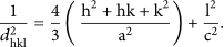
Observed 2θ Obs, reference 2θ Ref, β F W H M , the crystallite size (D), d h k l , and lattice parameter values from XRD analysis considering the peaks for hexagonal wurtzite (h) and monoclinic (m) crystal structures of metal oxide NP thin film samples for different spark‐discharge voltages (V S ).
h JCPDS no. 36–1451. m JCPDS no. 00‐043‐1038.
With the increase in spark voltage, smaller volumes of ZnO and Ag‐doped ZnO sample crystal structures were revealed. These peak shifts can not only correspond with the strain in the compound but also with the replacement of some Zn2+ ions with Ag ions, because Ag+, Ag2+, and Zn2+ ions have comparable ionic radii of 0.079 nm, 0.067 nm, and 0.073 nm, respectively. In addition, some Ag‐based oxide phases such as Ag2O and AgO can appear during the (Ag, Zn)‐based bimetallic oxide NPs formation. In some studies, the substitution of Ag ions into the ZnO lattice was observed in the site of Zn2+ or as an interstitial atom ion [44, 45]. In the case of silver ions replacing Zn2+ ions, a corresponding peak shift would be expected in the XRD pattern.
XRD patterns of Ag‐based oxide NP samples prepared with 4.3 kV and 7 kV spark voltages are shown in Figures 8 and 9. In this study, no diffraction peaks belonging to the free Ag phase were found in the samples. It was observed that Ag‐based metal oxide NP samples prepared under 4.3 kV and 7 kV spark voltage had a mixture of AgO and Ag2O oxide phases, showing atomic arrangements in different crystal structures. When the intensity and positions of the peaks appearing in the XRD patterns were examined, it was determined that the main (primary) phase was AgO (JCPDS no. 00‐043‐1038) with a monoclinic structure. It was observed that other phases contributing to the XRD results were Ag2O, which can have cubic (JCPDS no. 03‐065‐6811) and hexagonal (JCPDS no. 00‐019‐1155) structures, and AgO phases, which have a tetragonal (JCPDS no. 01‐084‐1108) structure. In the XRD patterns, evidence for the existence of other Ag‐based oxide phases other than AgO monoclinic can be noticed by the presence of small intensity extra peaks related to these phases, that is, splits and broadening of the peaks. However, broadenings in these peaks are generally located within the FWHM scale of a peak. For the Ag‐based oxide sample, the peaks observed at 30.430° (110), 30.610° (011), 31.827° (200), 33.061° (−102), 34.314° (002), 41.812° (210), 54.080° (−311), 66.472° (113), 68.645° (221), and 71.520° (004) for 7 kV spark voltage, and the peaks observed at 30.030° (110), 30.510° (011), 31.832° (200), 32.375° (−111), 34.237° (002), 41.397° (210), 50.410° (112), 52.790° (020), 61.910° (−221), 64.410° (022), 65.030° (−402), 66.370° (113), and 72.440° (004) for 4.3 kV clearly showed that the main phase was the AgO monoclinic structure. The most dominant peak in both samples comes from the (200)‐plane. As the spark voltage increased, the XRD peak intensities increased and the formation of the AgO monoclinic phase became more evident. For the Ag‐based oxide NP sample prepared under the influence of 7 kV spark voltage, there is a slight shift to the left in the (200)‐peak position, a 62% increase in the peak intensity, and an increase of around 11% in the FWHM value. This change corresponded with an increase in the a‐lattice parameter of the material at the same rate. Similar changes were observed in the (113)‐peak depending on the increase in spark voltage. When the spark voltage increased, the a‐lattice parameter of the AgO main phase as Ag‐based oxide increased, while the b‐ and c‐lattice parameters decreased. The increase in spark voltage resulted in AgO sample structures with smaller crystal volumes. The calculated lattice parameters of monoclinic Ag‐based oxide samples are given in Table 2. The d‐spacing (d
h
k
l
) values obtained from Bragg’s law have been used in the following expression for monoclinic system [43] and lattice parameters’ (a, b, c) calculations:

For 4.3 kV spark‐discharge voltage, XRD patterns of the Ag‐based oxide sample according to reference AgO and Ag2O mixture phases (red “+” for JCPDS no. 00‐043‐1038 of monoclinic‐AgO, green “△” for JCPDS no. 03‐065‐6811 of cubic‐Ag2O, blue “✳” for JCPDS no. 01‐084‐1108 of tetragonal‐AgO, and cyan “|” for JCPDS no. 00‐019‐1155 of hexagonal‐Ag2O). The “u” letter indicates an unknown phase and “⋆” symbols above the experimental peaks indicate corresponding to the diffraction peaks of the monoclinic‐AgO phase.
(b)


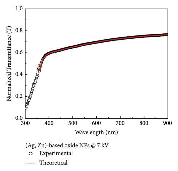
For 7 kV spark voltage, (a) experimental optical transmission spectra for Zn‐based, (Ag, Zn)‐based, Ag‐based oxide NPs, and glass substrate and (b) experimental and theoretical optical transmission spectra for (Ag, Zn)‐based oxide NPs.
(b)
Calculated film thickness t, optical band gap E g , resistivity ρ, optical absorption coefficient α, and figure of merit F M values of the metal‐based oxide NP thin film samples for spark‐discharge voltages V S .
Among the samples prepared under 7 kV, the Zn‐based oxide NP sample has the lowest optical transmission, depending on the metal ion it contains and film thickness. This is also the sample with the biggest film thickness (t Zn−based = 310 nm for 7 kV). The most optically transparent sample is the Ag‐based oxide NP sample. The film thickness of this sample (t Ag−based = 97 nm for 7 kV) is the smallest in this group (Table 3). Therefore, although there are structural differences in these samples, the small film thickness can also be considered as the reason for the high optical transmittance. In the sample prepared with a 7 kV spark voltage, a redshift was also observed at the absorption edge due to the effect of Ag ions entering the ZnO structure.
Other optical constants such as refractive index (n) and extinction coefficient (k) depending on wavelength can be obtained by the PUMA algorithm. The optical band gap (E
g
) of the semiconductor materials can be calculated with the help of the optical absorption coefficient (α = 4π
k/λ) and the Tauc method [48]. The Tauc method is based on the assumption that the energy‐dependent absorption coefficient α can be expressed by the following equation:

(αhν)2‐hν behavior of (a) Zn‐based, (b) Ag‐based, and (c) (Ag, Zn)‐based oxide NPs for 4.3 kV spark voltage.
(b)

(c)

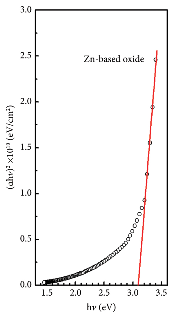
(αhν)2‐hν behavior of (a) Zn‐based, (b) Ag‐based, and (c) (Ag, Zn)‐based oxide NPs for 7 kV spark voltage.
(b)

(c)

The samples whose film thickness and optical band gap increased as the spark voltage increased were Zn‐based and (Ag, Zn)‐based oxide NP samples. The optical band gap of Ag‐based oxide NP samples increased as the spark voltage increased, but the film thickness decreased. In the samples prepared under both spark voltages, it was observed that the optical band gap narrowed due to the effect of Ag ions entering the ZnO structure. This contraction, which occurs due to the effect of Ag ions, is a sign of redshift. This can be explained by the presence of more absorption states or defective energy levels in the sample. This behavior is consistent with studies reported in the literature [49, 50]. Moreover, as the spark voltage increases, the difference between the optical band gap of Zn‐based and (Ag, Zn)‐based oxide NP samples also increases. The difference between the optical band gap of these samples prepared under 7 kV is 18.5%, while that of the samples prepared under 4.3 kV is 11.6% (Table 3).
Despite the smaller film thickness, this behavior of optical transmittance of Ag‐based oxide NP sample may be due to its different nanocrystal formations, which can also be called polyhedral‐shaped particles. Since this sample has the most differently shaped nanocrystal formations and amounts among the samples prepared with 4.3 kV spark voltage, therefore, the unusual change in its optical properties attracts attention. It is known that some metal oxide semiconductor materials having polyhedral nanoparticles with different sizes and facets can demonstrate different optical transmittance and band gap [37, 51, 52].
3.3. Electrical Properties
The figure of merit (F
M
), which is a measure of whether thin films can be used in optoelectronic applications, is determined by the resistivity (ρ) and the absorption coefficient (α) [53] as
Increasing this value requires that the materials in question have both low resistivity (high conductivity) and low optical absorption coefficient for the desired optical region. The optical transmittance values of the thin films consisting of nanoparticles, which are the subject of our studies, are quite high. In other words, optical absorption coefficients obtained from transmittance measurement (Table 3) are quite low.
According to the results obtained here, a decrease in resistivity values was observed with the addition of Ag. Since the optical band gap decreased with the addition of Ag into the ZnO host structure, band gap can be linked with resistivity. If both effects are taken into consideration together, with increasing spark‐discharge voltage, both the absorption coefficient and resistivity decrease and the figure of merit value increases. At least about a 2‐fold and 10‐fold increase in the figure of merit value was observed due to Ag entering into ZnO, for 4.3 kV and 7 kV spark‐discharge voltages, respectively. Therefore, it can be said that these films have the potential to be used in optoelectronic devices. There are studies in the literature with similar evaluations [25, 53].
4. Conclusions
In this study, Zn‐based, (Ag, Zn)‐based, and Ag‐based oxide NP thin film samples were successfully prepared using the spark‐discharge technique under different spark voltages. The effect of spark voltage on NP formation and crystal structure in the produced samples and its effect on optical properties were investigated. It was observed that Zn‐based and (Ag, Zn)‐based oxide samples prepared at different spark voltages had forms consisting of quasispherical nanocrystals. Nanocrystal sizes in Zn‐based and (Ag, Zn)‐based oxide samples were close to each other, and their sizes tended to increase with the increase in spark voltage. The size of the nanocrystal forms in Ag‐based oxide samples decreased as the spark voltage increased. In the Ag‐based oxide NP thin film sample prepared at low‐spark voltage (V S = 4.3 kV), there was a mixture of 3‐dimensional polyhedral‐shaped forms such as tetrahedron/octahedron, cubic, dodecahedron, and icosahedron. However, the fact that tetrahedron/octahedron‐shaped nanocrystals obtained with low‐spark voltage were not found in samples obtained with high‐spark voltage showed that low‐spark voltage was significantly effective in the formation of nanocrystals with this type of shape.
Both Zn‐based and (Ag, Zn)‐based oxide NP samples formed a hexagonal wurtzite structure with a dominant (100) peak when prepared under 4.3 kV spark voltage, and a dominant (002) peak when prepared under 7 kV. Here, it was found that the different planes of the same crystal structure came to the fore depending on the spark voltage value. This showed that the spark voltage had a very important effect on the crystal growth mechanism. Such that, when the spark voltage increased, the preferential orientation of the sample crystal structures was rearranged to be along the c‐axis instead of the a‐axis. In general, in metal oxide hexagonal wurtzite structures, preferential orientation occurred according to the higher crystal growth rates in the (100) and (002) planes. It was noteworthy that both spark voltages in this study were critical values that determined the competition of crystallographic orientations in metal oxide nanoparticle production. The intensity of the (200) peak belonging to the main AgO monoclinic structure of the Ag‐based oxide NP sample increased significantly with the spark voltage. This increase in the peak intensity was also noticeable in other peaks of the structure. 7 kV spark voltage revealed the monoclinic phase of the AgO compound more strongly, causing a slight increase in the a‐lattice parameter and a slight decrease in the b‐ and c‐lattice parameters. When monoclinic AgO was obtained with high‐spark voltage, it was formed in a crystal volume that was around 2.5% smaller. XRD analyzes indicated that the obtained Zn‐based, (Ag, Zn)‐based, and Ag‐based oxide NP thin film samples were formed as hexagonal wurtzite ZnO, hexagonal wurtzite Ag: ZnO, and monoclinic AgO phases.
The optical transmittance of samples varied considerably depending on the spark voltage. During the deposition process of AgO nanoparticles on the substrate surface, polyhedral‐shaped NPs with different sizes, shapes, and volumes could form in accordance with the nucleation criteria. Moreover, metal oxide semiconductors with polyhedral nanoparticles with different facets could also exhibit facet‐dependent optical properties. Related to this, there have been some studies showing that the optical band gaps of metal oxide materials decorated with dodecahedral‐shaped particles were larger. Therefore, a polyhedral‐shape dependent wider optical band gap could be expected for the AgO sample. Polyhedral‐shaped‐controlled optical and electrical conductive behavior in AgO samples could offer significant advantages. The film thickness and optical band gap of ZnO (Zn‐based oxide) and Ag: ZnO ((Ag, Zn)‐based bimetallic oxide) NP thin film samples increased significantly depending on the spark voltage. On the other hand, the optical band gap narrowed due to the effect of Ag ions entering the ZnO structure, regardless of the film thickness of these samples. The narrowing of the band gap resulting from the effect of Ag ions indicated a redshift. As a result, it was observed that the preferential orientation in the crystal, optical band gap, nanoparticle forms and their distributions changed strongly depending on the spark voltage.
Data Availability
The data used to support the findings of this study are included within the article.
Conflicts of Interest
The authors declare that they have no conflicts of interest.
Footnotes
Acknowledgments
This study was supported by the Scientific and Technological Research Council of Turkey (project no. 116F046) and the Scientific Research Unit of Burdur Mehmet Akif Ersoy University (project nos. 110‐NAP‐10, 100‐NAP‐10, 172‐NAP‐13, 173‐NAP‐13, 0324‐NAP‐16, 0253‐MP‐14, 0815‐MP‐22, 0799‐MP‐21, and 0804‐MP‐21).