
Abstract
Nanostructures of undoped zinc oxide and nickel‐doped zinc oxide (Ni = Zn0.98Ni0.02O, Zn0.96Ni0.04O, and Zn0.94Ni0.06O) were synthesized by using the coprecipitation process, and their optical and dielectric properties were simultaneously investigated. The XRD results confirm the hexagonal structure having space group P63mc. By increasing nickel concentration, the particle size decreases, while the strain is increased. Fourier‐transform infrared (FTIR) analysis was carried out in order to learn more about the phonon modes present in nickel‐doped zinc oxide. UV‐Vis spectroscopy further revealed that the optical band gap of nickel‐doped samples varied from 3.18 eV to 2.80 eV. The SEM analysis confirms the rod shape morphology of the already synthesized samples. EDX analysis investigates the incorporation of nickel ions into the zinc oxide lattice. Using photoluminescence spectroscopy, we found that the synthesized materials had oxygen vacancies (Vo) and zinc interstitial (Zni) defects. Dielectric constant (ε r) and dielectric loss (ε) are both improved in nickel‐doped zinc oxide compared to undoped zinc oxide. Since more charge carriers enhanced after the nickel ions were exchanged for the Zn ions, the AC electrical conductivity (σ a.c) improves by nickel doping compared to undoped zinc oxide.
1. Introduction
Transition metal oxide compounds have some special characteristics among which zinc oxide is an interesting n‐type semiconductor with a wide band gap of 3.37 eV and a maximum exciton binding energy of 60 meV. Due to its unique properties like nontoxicity, easy synthesis, low cost, and good electrical and thermal stability, it is a promising compound for various optoelectronic applications, i.e., solar cells [1–3], UV photo detectors [4], UV absorbers [5], LEDs [6–8], capacitors, battery electrodes [9], sensors [10–12], resonators, and TCO [13], and also can be used as photocatalyst [14].
For various optoelectronic purposes, zinc oxide is doped with transition metals (Fe, Co, Ni, Cu, etc.) among which nickel is the most promising candidate due to its extreme stability. Numerous research studies have been conducted to explore the different properties of zinc oxide through a number of dopants. However, nickel‐doped zinc oxide is a good candidate owing to its good photonic ability, high electrical conductivity, and good chemical stability. Therefore, nickel‐doped zinc oxide has high dielectric constant and low dielectric loss as compared to undoped zinc oxide and has significant electrical conductivity which makes it a promising candidate for optoelectronic applications. The introduction of various defects in metal oxides has a great influence on their band structure and donor densities and hence influences optical and dielectric properties [15]. Zinc oxide exhibits numerous induced defects, with the most favorable ones being the oxygen vacancies labeled as Vo [16]. Many experimental and theoretical works showed that the electronic charge transport, band structure, and surface properties are mostly attributed to Vo. The improvement in charge generation and separation is attributed to the presence of isolated energy levels resulting from the influence of Vo [17, 18]. In addition, oxygen vacancies are recognized as dynamic sites for surface adsorption and desorption phenomena [19, 20]. Recently, a lot of research was carried out for the stable synthesis of zinc oxide for investigating its optical and dielectric behavior.
Many routes like hydrothermal method [21], metal organic chemical vapor deposition [22], polyol method [4, 23], sol‐gel [24], solution combustion [25], coprecipitation [26, 27], carbothermal evaporation [28], and electrodeposition [29] methods are used to synthesize zinc oxide nanostructures. Among the mentioned methods, the coprecipitation method has the advantage of greater yield, low temperature synthesis, and greater reaction properties. In the present work, we have prepared pure and nickel‐doped zinc oxide nanostructures via the chemical coprecipitation method. The aim of the study is to investigate the optical and dielectric properties of the prepared samples for various optoelectronic applications. Nickel‐doped zinc oxide nanostructures showed enhanced dielectric constant, high electrical conductivity, and low dielectric loss due to various defects such as V0 and Zni. It is noteworthy that, prior to this, there had been limited research on oxygen vacancies to demonstrate the optical and dielectric properties of nickel‐doped zinc oxide [30–32]. Hence, our explored results show that nickel‐doped zinc oxide can be a favorable candidate for various optoelectronic applications.
2. Experimental
2.1. Chemicals
Zinc acetate dihydrate [Zn(CH3COO)2.2H2O], nickel chloride hexahydrate (NiCl2.6H2O), KOH, and DI water were used for the preparation of samples. All the chemicals were purchased from Sigma‐Aldrich with 99% purity.
2.2. Sample Preparation
The pure zinc oxide and Zn0.98Ni0.02O, Zn0.96Ni0.04O, and Zn0.94Ni0.06O nickel‐doped samples were synthesized by the chemical wet coprecipitation method.
2.202 g of zinc acetate dihydrate [Zn(CH3COO)2.2H2O] was dissolved in 100 ml DI water, and then 1.125 g of KOH was dissolved in 10 ml DI water. The KOH solution was dropwise added to the zinc acetate solution under vigorous stirring. The precipitate was then put on hot plate for 3 hours at 70°C. The temperature was kept constant, and the reaction was carried out. The obtained white precipitate was then washed with DI water by centrifugation and then then dried at 80°C for 24 hours. The prepared powder was then annealed in a furnace for 4 hours at 600°C. The same experiment was performed several times, and the same results were obtained with controlled synthesis. The synthesis diagram is given in Figure 1. The chemical reaction is given below:


Synthesis diagram for the preparation of undoped and nickel‐doped zinc oxide.
(b)

(c)

Different lattice parameters of pure zinc oxide and nickel‐doped zinc oxide.
By utilizing the formula mentioned above, it was noticed that a decrease in crystallite size and an increase in nickel concentration resulted an increase in the calculated strain from 3 × 10⁻⁴ to 3.6 × 10⁻⁴ [31]. The crystallite density is calculated from the following formula [34, 35]:
The calculated crystallite density varies from 1.1 × 10¹¹(cm)−2 to 1.7 × 10¹¹(cm)−2 for undoped and nickel‐doped zinc oxide, respectively. Different lattice parameters are shown in Table 1. Crystallite density versus microstrain graph is given in Figure 2(c).
3.2. SEM and EDX Analysis
Morphological and elemental composition study was carried out through scanning electron microscopy. Figure 3 shows the SEM micrographs of undoped and nickel‐doped zinc oxide. From the SEM micrographs, it is clear that rod‐like morphologies are formed for both the undoped and nickel‐doped samples. The rods showed some variability which is due to the doping of Ni into ZnO lattice. The particle size was seen to decrease with increasing nickel concentration, and the same was reported in [36, 37].

(a–d) SEM images of pure and nickel‐doped zinc oxide and the other four are EDX images of pure and nickel‐doped zinc oxide.
(b)
3.5. Photoluminescence (PL) Spectroscopy
At room temperature using a PL spectrometer, we were able to acquire the PL emission spectra of both undoped and nickel‐doped zinc oxide across the wavelength range of 200–800 nm. All the samples were excited at 340 nm. There are emission observations in two different regions: one in the ultraviolet range and the other in the visible range. PL spectra are shown in Figure 6, along with their respective nickel contents. The reason for the emission peak being observed at 395 nm [32] is because of the free exciton emission that occurs in the zinc oxide nanostructures. The transition of an electron from a narrow donor level of Zni to the uppermost valence band correlates to the violet absorption peak that occurs at around 412 nm [33, 39]. It is believed that singly ionized zinc or other inherent defects are responsible for the blue [4, 35] emission peak that occurs about 451 nm. There is a possibility that singly ionized oxygen defects are responsible for the peak that is found in the green spectrum about 558 nm [21]. The peaks that appear in the red [40] region around 640–680 nm are attributed to electron recombination that occurs between the donor level and the acceptor level. The donor level is associated with oxygen defects, and the acceptor level is associated with vacancies, particularly as a result of doping. The various peak shifts due to nickel doping are given in Table 3.
PL emission spectra of undoped and nickel‐doped zinc oxide.

Position of PL emission peaks of undoped and nickel doped zinc oxide.
It was noted that in the doped samples, there are least defects in the undoped zinc oxide sample having less intense spectra, while there are a large number of vacancies in the Zn0.94Ni0.06O sample presenting more intense emission spectrum. The various vacancies were validated by the Pl emission spectra. These findings are linked to the UV‐visible absorption spectra for both samples which exhibited low and high absorption, respectively, as well as the results of the SEM examination, which revealed that the rods in the Zn0.94Ni0.06O sample did not develop properly owing to the higher nickel content.
3.6. Dielectric Properties
3.6.1. Dielectric Constant
The frequency dependence of the dielectric constant for undoped zinc oxide and nickel‐doped zinc oxide that has been annealed at 600°C is shown in Figure 7. Using a pellet presser, the produced samples were compressed into the shape of circular pellets, from which the capacitance, dielectric loss, and alternating current conductivity were measured as a function of frequency. Capacitance was measured by stacking silver paste electrodes on top of the pellets to make a circular parallel plate. To calculate the dielectric constant of both undoped and nickel‐doped zinc oxide, the following equation was used:
Frequency‐dependent dielectric constant of undoped and nickel‐doped zinc oxide.

The ε
r values of both undoped and nickel‐doped zinc oxide were found to decrease with frequency up to 1 × 10³ Hz. At higher frequencies, the values of
As expected, the Zn0.94Ni0.06O nickel‐doped zinc oxide sample has the highest dielectric constant of all the synthesized samples, with the undoped zinc oxide sample having the lowest. When the nickel content was enhanced, oxygen vacancies increased, leading to a higher dielectric constant. EDX and photoluminescence study indicated that the Zn0.94Ni0.06O nickel‐doped sample contains the maximum amount of vacancies and hence displays the highest dielectric constant.
3.6.2. Dielectric Loss
Figure 8 depicts the frequency‐dependent change in dielectric loss,
Frequency‐dependent dielectric loss of undoped and nickel‐doped zinc oxide.

Pure zinc oxide has the maximum dielectric loss among the synthesized samples, whereas the Zn0.94Ni0.06O nickel‐doped zinc oxide sample has the lowest dielectric constant due to its higher nickel content. As nickel concentration rose, dielectric loss reduced. The lowest dielectric loss was seen in the Zn0.94Ni0.06O nickel‐doped sample, which was validated by EDX and photoluminescence analysis to have the maximum number of vacancies, leading to greater conduction of charges.
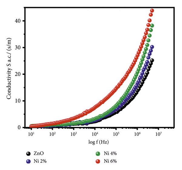
3.6.3. Electrical Conductivity
Figure 9 depicts the electrical conductivity of undoped and nickel‐doped zinc oxide nanostructures as a function of frequency for an alternating current. It is often believed, and supported by research [44], that AC electrical conductivity increases as frequency increases. The electrical conductivity of all the samples is almost nil at very low frequencies, rising steadily with increasing frequencies and then dramatically increasing at extremely high frequencies. The Maxwell–Wagner interfacial model can explain this frequency‐dependent conductivity performance. The charge carriers are met with resistance at the grain boundaries. These ions are free to move about inside the grains, but their resistive nature prevents them from leaving the grains. The little increase in conductivity at low frequencies can result from the tunneling or hopping effect, and charge carriers might be transported by an endless number of pathways between grains. In order to promote conductivity, a material needs a high frequency so that the charge transporters have enough energy to overcome the barriers, freeing the charges. When nickel is introduced into the Zn1−xNixO lattice, a significant number of charge transporters are generated, leading to an increase in conductivity. The AC conductivity of undoped and nickel‐doped zinc oxide is calculated using the following formula:
Frequency‐dependent AC electrical conductivity of undoped and nickel‐doped zinc oxide.
Since (ω = 2πf) f is the frequency, (σ
a.c) is the electrical conductivity of alternating current, (
Since the dielectric loss decreases with frequency while the conductivity increases, it is obvious from the preceding equation that the tangent loss alone determines the AC conductivity. This result is consistent with the literature, which demonstrates that a series of opposing effects [44] support the trend of increased σ a.c with higher frequencies.
There are two possible explanations for this increase in AC electrical conductivity: either the electrical energy associated with a high AC frequency applied field enables charge transporters to hop between the nanostructures, or the polarization of zinc oxide nanoparticles is reduced to a greater extent at higher frequencies, making the material more dielectric. When the concentration of the dopant is increased, more oxygen vacancies are created, which bind the charge transporters. The supplied field has a lot of energy at higher frequencies, and hence the AC conductivity increases suddenly as a result of the discharge of these charges. Therefore, a rise in nickel content leads to an increase in oxygen vacancies, which in turn increases the density of charge carriers and the AC conductivity of the material. When it comes to the AC conductivity of our manufactured samples, Zn0.94Ni0.06O nickel‐doped zinc oxide comes out on top, followed by Zn0.96Ni0.04O and Zn0.98Ni0.02O doped samples with the maximum number of oxygen vacancies, respectively, while undoped zinc oxide has the lowest.
4. Conclusion
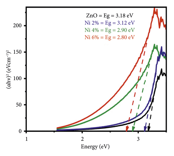
The undoped and nickel‐doped zinc oxide nanostructures were prepared by the chemical wet precipitation method. XRD analysis confirmed the only hexagonal wurtzite structure without any other impurity phase of Zn, Ni, and NiO. EDX confirmed the substitution of nickel into the host zinc oxide lattice in different concentrations. UV‐Vis spectroscopy revealed that nickel was present in octahedral symmetry without disrupting the wurtzite structure, and a red shift was due to the incorporation of nickel into zinc oxide matrix. PL showed various defects density, and the red shift observed was due to the doping of nickel in the zinc oxide lattice, attributed to the sp‐d exchange interactions of the localized and band electrons of the nickel. Dielectric properties showed enhancement as the dielectric constant was increased with nickel doping and the dielectric loss was decreased. AC electrical conductivity also showed increase in the nickel‐doped zinc oxide. Hence, after investigating various optical and dielectric properties, nickel‐doped zinc oxide may be a helpful compound for various optical and frequency‐dependent applications.
Data Availability
The data used to support the findings of this study are available from the corresponding authors upon request.
Ethical Approval
This research was conducted in a legal and ethical way and is completely in compliance with the ethical standards.
Conflicts of Interest
The authors declare that they have no conflicts of interest.
Authors’ Contributions
All the authors contributed equally to this work.