
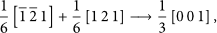
Abstract
Multigroup large‐scalenanocutting models of monocrystalline Cu were established by molecular dynamics simulations to investigate the influence of cutting parameters on the material removal mechanism. The formation and distribution of subsurface defect structures were revealed, and the evolution behavior of the complete prismatic dislocation loop was analyzed in depth. It was demonstrated that the chips and machined surface of monocrystalline Cu were mainly formed under the coupling effect of shearing and extrusion forces. A diamond tool with a larger edge radius or a negative rake angle could produce a noticeable suppression on the chip formation. The corresponding relationship between the location of defect atoms and the distribution of von Mises stress was studied, which indicated that the shear stress would become larger at the subgrain boundaries, dislocation lines, and the amorphous atoms than that in their nearby regions. The complete prismatic dislocation loop was formed by cross‐slip between two sets of stacking faults; meanwhile, the generated multiple Lomer–Cottrell locks hindered its movement and promoted the work‐hardening phenomenon. These research results are of great theoretical value to enrich the nanocutting mechanism and technology of plastic materials.
1. Introduction
Monocrystalline Cu not only has better toughness and lower resistivity but also has almost lossless signal transmission properties due to the lack of grain boundaries that hinder and attenuate the signal. Therefore, it is widely applied in various fields such as laser optics, linear accelerators, microelectronics, and semiconductor technology. In recent years, many researchers had investigated the material removal mechanism of monocrystalline Cu during nanomachining through various methods, including experiments and molecular dynamics simulation (MDs). When the characteristic size reaches the nanoscale, there exist certain material deformation behaviors which are different from those at the macroscopic scale due to the size effect [1–3]. Results reveal that in addition to cutting parameters (e.g., cutting speed [4] and cutting depth [5]), tool geometry [6, 7], loading modes [8, 9], and anisotropy [10, 11] also have considerable effects on the material removal mechanism and subsurface defects of monocrystalline Cu. Zhang et al. [12] studied the effect of cutting depth and cutting speed on the dislocation nucleation within the subsurface by MDs, and it was found that the increase in cutting speed and cutting depth contributed to the formation of the stair‐rod dislocation and Hirth dislocation. Zhu et al. [13] adopted the finite element method to simulate a nanoscratching process of monocrystalline Cu. Although monocrystalline Cu shows good machinability by ultraprecision machining, the machined component is commonly accompanied by surface defects such as burrs and steps, which seriously affect the shape accuracy and surface quality of the workpiece. The reasons for this phenomenon are as follows. For one thing, a large number of dislocation nucleation, multiplication, and motion (slip and climb) have arisen within the workpiece under the extrusion and shear of the tool during machining. Some dislocations, such as half dislocation loops, are annihilated after moving to the free surface so that a certain degree of atomic‐level steps appears on the machined surface [14]. For another, the monocrystalline Cu atoms are bonded by metallic bonds which are tough and less prone to fracture, so that the chips commonly exist in a band form and there appear burrs on both sides of the tool.
Furthermore, due to the interaction among dislocations which occurs by means of dislocation jog, dislocation kink, and cross‐slip, various subsurface defects can be generated, thus causing permanent plastic deformation and severely affecting its working life [15], for instance, atomic cluster [16], prismatic dislocation [17], Lomer–Cottrell lock [18], prismatic dislocation loop [19], and stacking fault tetrahedron (SFT) [20]. Li et al. [21] carried out nanocutting simulations of γ‐TiAl alloy under fluid media and analyzed the evolution of the prismatic dislocation loop, subsequently indicating that the formation of subsurface defects led to the work‐hardening phenomenon adopting nanoindentation as the characterization method, with the indentation load, surface hardness, and Young’s modulus as the evaluation indicators. Liu et al. [22] conducted real‐time observation of SFT formation and annihilation processes in terms of dislocation reactions. They found that SFT evolution underwent multiple stress fluctuations and also pointed out that the formation of SFT was one of the reasons for the work‐hardening effect.
As mentioned above, it can be seen that few scholars established large‐scale models to simulate the nanocutting process of monocrystalline Cu. Therefore, in this paper, four parts of contents were studied and discussed in Section 3. First, the chip formation and machined surface were analyzed (Section 3.1), and the relationship between the subsurface defects in the cutting process and the von Mises stress was revealed by the atomic stress analysis (Section 3.2). On this basis, to further clarify the machining‐induced internal defects of monocrystalline Cu, the 3D nanocutting models were developed to reveal the evolution of the prismatic dislocation loop during the nanocutting process (Sections 3.3 and 3.4), which was analyzed with the dislocation extraction algorithm (DXA) [23].
2. MD Modeling
Seven groups of 2.5D nanocutting simulations of monocrystalline Cu were conducted by LAMMPS. According to the cutting variables, the original simulations were divided into three modules: A, B, and C. The cutting variables and assigned parameters are listed in Table 1. Note that the group no. 4 in Module B and the group no. 6 in Module C were the same. Figure 1 displays a 2.5D nanocutting model of monocrystalline Cu, corresponding to the values of the tool rake angle r in the Module A simulation. The monocrystalline Cu workpiece was composed of 3512294 atoms with dimensions of 177.1 nm × 91.4 nm × 2.5305 nm along the x, y, and z directions, which corresponded to the crystal directions [1 0 0], [0 1 0], and [0 0 1], respectively. To avoid the influence of anisotropy on the research results, all the nanocutting simulations were performed on the (0 1 0) crystal plane along the [

The cutting variables and assigned parameters corresponding to 2.5D simulations of monocrystalline Cu.

2.5D nanocutting model of monocrystalline Cu.
To make the lattice structure close to the actual working conditions, the energy minimization was first carried out with the conjugate gradient method to eliminate the unreasonable factors in the initial model. The 2.5D monocrystalline Cu model was then relaxed successively using the NPT and NVT ensemble to reach an initial temperature of 293 K and a stable initial pressure of around 0 bar. The velocity calibration method was used to precisely regulate the temperature of the thermostatic layer throughout the cutting process. The Morse [17] and EAM [24] potential functions were adopted to describe the interactions between both Cu‐Cu and C‐Cu, respectively. The diamond tool was set as a rigid body, and therefore, the movement of its internal atoms was negligible. Additionally, Figure 2 presents one of the 3D nanocutting models of monocrystalline Cu, with the cutting parameters as shown in Table 2. The rest of the simulation parameters are kept consistent with those in the 2.5D simulation models.

3D nanocutting model of monocrystalline Cu.
3D nanocutting parameters of monocrystalline Cu.
The EAM potential function is defined by the following equations:
The Morse potential is used to describe the atomic interactions in the system by the following equation:
In this study, the transient response data during the nanocutting process were analyzed and rendered by the OVITO [25] software. The common neighbor analysis (CNA) [26] and DXA were applied to analyze the distribution of both crystal structures and subsurface defects.
3. Results and Discussion
3.1. Chip Formation and Machined Surface
Figure 3 shows the statistics of chip atomic numbers for different cutting parameters. From Figure 3(a), the number of chip atoms decreased as the tool edge radius increased. As a result of the edge effect, the contact surface between the tool and the workpiece changed as the tool edge radius increased, so that the tool edge gradually became the main part of the contact surface. At this point, the extrusion force provided by the tool started to play a critical role. A growing tool edge radius can increase the effective negative rake angle of the tool, thus subjecting the material in front of the tool to a greater squeezing effect, which in turn suppresses the chip formation [27]. The variation of the chip atomic number with the cutting speed is illustrated in Figure 3(b). It can be observed that the effect of cutting speed on the chip atomic number was unstable. Specifically, when the cutting speed increased from v 1 to v 2, the chip atomic number remained essentially unchanged, but when the cutting speed increased from v 2 to v 3, the chip atomic number decreased significantly. The distribution of the chip atoms increments between v 1 and v 2 at the same cutting distance is presented in Figure 3(c), which corresponds to different tool edge radii. The average value in the box plot indicated that the chip atom increments between the two cutting speeds were negligible compared to the total chip atomic number. Therefore, when the nanocutting was performed at v 1 or v 2 with each tool edge radius, the numbers of chip atoms were basically identical. The chip atoms were evidently reduced when the rake angle r was −15° using a tool with an edge radius of 30 nm, as shown in Figure 3(a). The reason was that the existence of the negative rake angle further contributed to the effective negative rake angle of the tool, which resulted in a reduction of the chip atomic number. Consequently, the chip formation was remarkably suppressed under the coupling effect of the increasing edge radius and the negative rake angle of the tool.

Statistics of chip atomic number for different cutting parameters: (a) tool edge radius and rake angle, (b) cutting speed, and (c) difference value in number of chip atoms between v 1 and v 2.
(b)
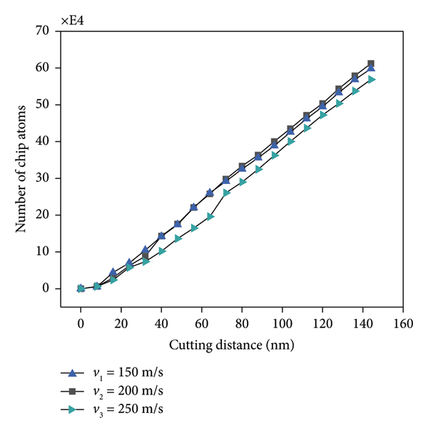
(c)

The distribution of atomic displacements along the x‐ and y‐directions at a cutting distance of 72.9 nm is visualized in Figure 4 (Simulation No. 3), which refers to the atomic displacements at a cutting distance of 16.2 nm. The unannotated black arrows in the snapshot represented the direction of the displacement vectors in the local region, and the unclosed dashed box corresponded to the workpiece surface. First, the workpiece atoms near the tool rake face moved forward along the x‐direction accompanied by the displacement in the y‐direction being zero, while the atoms near the cutting edge started to move downwards and to the right due to the extrusion and shearing. Then, as the nanocutting proceeded, the chips which initially formed on the rake face began to move upwards to the right under the friction action, while the atoms under the flank face moved passively downwards to the right under the extrusion and frictional forces. At the same time, a small bulge was formed beneath the flank face under the tensile stress and disappeared with the release of pressure. It can also be observed that the atoms of the machined surface moved downwards to the right under the tool extrusion, causing the height of the machined surface to be obviously lower than the flank face. No obvious surface recovery was detected, which had a great difference with the ductile region machining of semiconductor materials [28]. The main explanation for this difference was that the Cu atoms were bonded by the long‐range metallic bonds, where the interatomic forces were not prone to disappear, i.e., the Cu‐Cu bonds were not easy to break, which well explained the reason why the side flow phenomenon and significant surface recovery did not occur on the surface of monocrystalline Cu. Besides, the atoms within the shear‐slip zone ahead of the chip were subjected to dislocation extensions along [


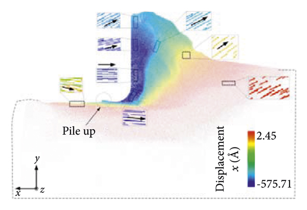
Distribution of atomic displacements at a cutting distance of 72.9 nm. (a) Displacement x and (b) displacement y.
(b)

3.2. Stress Analysis
Figure 5 shows the distributions of von Mises stress and the crystal structures in the workpiece using a tool with an edge radius of 10 nm, which reflected the internal relationship between the atomic stress state and the crystal structure. Under the shearing and extrusion actions, there appeared many blocky crystals in front of the tool, which generated their respective subgrain boundary with continuous amorphous atoms, further constituting the subgrains. The von Mises stress value was maximum (at least 15 GPa) at the subgrain boundary (Figure 5(a)). In addition, many stacking faults along the different slip systems appeared in the subsurface and the shear‐slip zone, and their respective boundaries (i.e., dislocations) were formed with discontinuous amorphous atoms. This result revealed that the stress value at the dislocations in the subsurface was obviously larger than that in the nearby region (approximately 11 GPa), while the stress value at the foremost Shockley partial dislocations was only 8‐9 GPa. The reason was that massive dislocation block networks were generated at the bottom of the subsurface, which prevented the movement of the dislocations and accordingly increased the stress value, as seen in the subgraphs A and B in Figure 5(b). Meanwhile, under the extrusion action by the tool, many interstitial atoms were formed and distributed in the three major deformation zones with a stress range of 12‐13 GPa, whereas the stress value at the point defects below the subsurface deformation zone was about 8.5 GPa. As the tool moved forward, the atoms in the flank friction zone transformed into the amorphous structure under the extrusion and friction of the flank face, with a stress value of about 17–19 GPa. Notably, the atomic stress distribution could reflect the location of subsurface defects with stress values of around 10‐11 GPa. Subsurface defects in Figure 5 were mainly stair‐rod dislocations and prismatic dislocation loops. In contrast to the subsurface defects mentioned above, there were no significant stress distribution characteristics with a stress value lower than 8 GPa because of the more uniform stress distribution at the stacking faults. Therefore, the formation of stacking faults could not be determined only from the perspective of von Mises stress. The initially nucleated dislocations moved forward fast in the form of dislocation extensions. Some dislocations underwent annihilation under the interactions, and the rest eventually continued to slip in the form of dislocation emission until they approached the boundary layer, as depicted in Figures 5(c) and 5(d). Accordingly, from the distribution of the crystal structures and von Mises stress, it revealed that a greater shear stress would distribute at the subgrain boundaries, dislocation lines, interstitial atoms, and subsurface defects during nanocutting. In the stable cutting stage, along with the movement of numerous dislocations, the plastic deformation of the workpiece occurred mainly along the horizontal direction, and the depth of the deformation layer in the y‐direction tended to be stable, with a maximum depth of about 25‐26 nm, as shown in Figure 5(d). The reasons for the phenomenon will be explained in detail in the next section.

The variations of the von Mises stress and crystal structures with cutting distance of (a and c) 53.46 nm and (b and d) 72.9 nm. The subgraph (A–C) shows the distribution of the dislocation lines and subgrain boundaries in the three deformation zones, respectively.
3.3. Subsurface Defect Structure
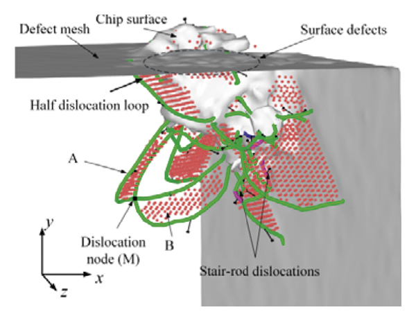
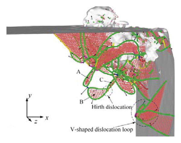
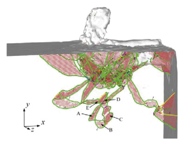
Figure 6 shows the crystal structure distribution inside the workpiece from simulation no. 7, where the cutting distance was located at 72 nm. The atoms with both diamond and FCC lattice structures were hidden in order to clearly observe the subsurface defects distribution. The HCP, BCC, and other crystal structures were colored in accordance with that in Figure 5. It was apparent that the original lattice structures underwent the atomic misalignment under the action of accumulated strain energy, which in turn formed numerous stacking faults and dislocations, followed by moving along the {1 1 0} <1 1 0> slip systems. Stacking faults formed by different stacking ways were separated by dislocation lines (i.e., the boundaries of stacking faults) so that there coexisted multiple crystal structures inside the workpiece. However, based on the x‐ycross‐section view of the crystal structures, only slip directions of the stacking faults could be indicated, but no close‐packed faces and 3D defect structures inside the subsurface could be detected. Thus, the slip planes and subsurface defect structures were prominently marked in Figure 6.
The crystal structure distribution at a cutting distance of 72 nm inside the workpiece by the CNA method.
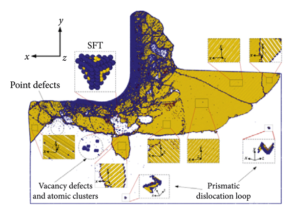
The dislocation annihilation induced by the interaction of dislocations below the tool edge was responsible for the partial recovery of the stacking faults to the original FCC lattice structure, which further verified the result that dislocation annihilation was one of the inducements of dislocation emission. Many subsurface defect structures, including prismatic dislocation loops, SFT, V‐shaped dislocations, interstitial atoms, vacancy defects, and atomic clusters, were formed inside the workpiece under the interaction of various oriented stacking faults, which seriously affected the service life of the workpiece and the dimensional accuracy of the machined surface. Several typical subsurface defects during nanocutting of 2.5D monocrystalline Cu were depicted in Figure 7 to present their formation principles.

Schematic diagram of several typical subsurface defect structures.
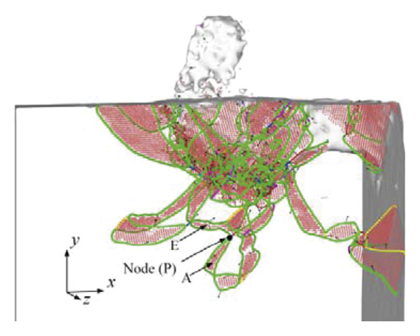
To clearly present the distribution of various dislocations and their interactions, the DXA method was employed to display the distribution of the dislocations and subsurface defect structures, as shown in Figure 8. The blue defect meshes represented the defect surfaces and subgrain boundaries. During the movement of the dislocations, a perfect dislocation had to be decomposed into two Shockley partial dislocations, enabling the consumed energy to be lower, which was called dislocation extension. The extended dislocation was made up of two Shockley partial dislocations, and the stacking faults sandwiched between them. The dislocation reactions followed the rule from equation (3). From Figures 7 and 8, it was evident that SFT was composed of six stair‐rod dislocations. Lomer–Cottrell (L‐C) dislocation and Hirth obstruction consisted of two extended dislocations and one stair‐rod dislocation or Hirth dislocation, respectively. The difference between these two forms of sessile dislocation configuration was that the angle between the two stacking faults connected to the stair‐rod dislocation was distinct from that connected to the Hirth dislocation (acute and obtuse angle, respectively) [21]. In this study, the Thompson tetrahedron was adopted to describe the dislocation reactions for the FCC lattice structure [29]. The formation of the two dislocation configurations mentioned above followed the reaction laws of equations (4) and (5). The prismatic dislocation loop contained at least one L‐C dislocation. The V‐shaped dislocation comprised two extended dislocations and one sessile or perfect dislocation, where the two stacking faults generally extended towards the free surface and formed atomic‐level steps. Although the vacancy defects can cause distortion of the lattice structure, the crystal free energy would be reduced accordingly with their consecutive formation, enabling the crystal structure to reach a stable state again.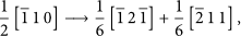


The distribution of the dislocations and subsurface defect structures at a cutting distance of 72 nm.
Note that there were many dislocation networks at the boundaries of the subsurface deformation zone, which restrained the expansion of the subsurface deformation zone into the interior of the workpiece, thus greatly suppressing the plastic deformation. This was also the reason why the depth of the subsurface deformation zone in Figure 5 was stable at 25‐26 nm. In contrast, the dislocation extension along the x‐direction was very fast. The reasons were as follows: first, monocrystalline Cu had extremely high ductility and was sensitive to plastic deformation due to its deformation mechanism of shear slip. Second, the tool only moved linearly along the x‐direction, and the tangential force was apparently dominant. Third, the motion of the dislocations and their interaction became more complex due to the large cutting parameters used in this study. The periodic boundary conditions allowed the stacking faults, which should move along the z‐direction, to accumulate in front of the chip, so as to inevitably accelerate the rate of dislocation extension.
3.4. Evolution of the Prismatic Dislocation Loop
Because the complete 3D morphology of the subsurface defect structures cannot be detected from the aforementioned results, 3D simulations were conducted to explore the evolution of complete subsurface defects inside the workpiece. Figure 9 shows the atomic structure and dislocation composition of the prismatic dislocation loop. The prismatic dislocation loop was a plane defect that generated by the cross‐slip of four stacking faults A, B, C, and D along their respective slip systems. Meanwhile, the sessile dislocations in the dislocation loop and the extended dislocations on each side constituted two dislocation configurations, that is, L‐C dislocation and Hirth obstruction.

Atomic structure and dislocation composition of the prismatic dislocation loop.
(b)

The formation of the prismatic dislocation loop inside the subsurface during nanocutting was analyzed by DXA as shown in Figure 10. The different types of dislocations were distinguished by their corresponding colors, as listed in Table 3. It can be seen that when the cutting distance reached 4.4 nm (Figure 10(a)), diverse stacking faults in the shear‐slip zone exhibited significant slip and movement along the {1 1 1} <1 1 0> systems due to the shearing and extrusion action from the tool. During the dislocation extension process, the two stacking faults (1 


The evolution of prismatic dislocation loop at the cutting distances of (a) 4.4 nm, (b) 6.6 nm, (c) 7 nm, (d) 8.6 nm, (e) 8.8 nm, (f) 9.0 nm, (g) 9.2 nm, (h) 9.4 nm, (i) 10 nm, and (j) 12 nm.
(b)

(c)
(d)

(e)

(f)

(g)

(h)

(i)

(j)

Dislocation types and their Berger vectors inside the subsurface of Cu.
To further study the evolution of the prismatic dislocation loop, its annihilation process during nanocutting was analyzed as shown in Figure 11. When the cutting distance reached 15 nm (Figure 11(k)), compared to the result in Figure 10(j), it started to move towards the dislocation group along the [1 1 0] direction. Under the shear stress, as the prismatic dislocation loop moved upwards and interacted with the dislocation group, the suppression effect of sessile dislocations on the dislocation slip was greatly weakened. From Figures 11(l) and 11(m), the 1/6 [1 2 


The annihilation process of the prismatic dislocation loop at the cutting distance of (k) 15 nm, (l) 15.2 nm, (m) 15.4 nm, (n) 15.8 nm, (o) 16 nm, and (p) 18 nm (the order number of a subgraph is continuous with that in Figure 10).
(l)

(m)

(n)
(o)
(p)

4. Conclusions
Multiple nanocutting simulations of monocrystalline Cu were conducted by MDs in this paper. Not only the effect of simulation parameters, such as the tool edge radius, rake angle, and cutting speed, on the formation of chips and the machined surface was investigated but also the structural composition of various typical subsurface defects was revealed. Also, the evolution of the prismatic dislocation loop was studied in depth. The main conclusions are summarized as follows. The chips and machined surface of monocrystalline Cu are mainly formed under the coupling effect of shearing and extrusion forces. In nanocutting, a diamond tool with a larger edge radius or a larger negative rake angle can produce a noticeable suppression of the chip formation. The surface recovery of plastic material is caused by the motion of partial dislocations towards the free surface, while, for the brittle material, it is induced by the motion of amorphous atoms towards the machined surface. This distinction is determined by the bonging form among atoms inside the two materials. In nanocutting of monocrystalline Cu, there exist many defective structures inside the subsurface, which has a serious impact on the surface morphology and subsurface quality, which is the internal factor of the work‐hardening effect. The corresponding relationship between the location of defect atoms and the distribution of von Mises stress indicates that the shear stress would be larger at the subgrain boundaries, dislocation lines, and the amorphous atoms than that in their nearby regions.
Data Availability
The data used to support the findings of this study are available from the corresponding author upon request.
Conflicts of Interest
The authors declare that they have no conflicts of interest in this article.
Authors’ Contributions
All listed authors have made a significant scientific contribution to the research in the manuscript and approved its claims. All authors confirmed the final authorship for this manscript.
Footnotes
Acknowledgments
The authors disclose receipt of the following financial support for the research, authorship, and/or publication of this article. This work was supported by the National Natural Science Foundation of China (Grant no. 51805371) and the Tianjin Research Innovation Project for Postgraduate Students (Grant no. 2021YJSS289). The authors thank the MNMT lab for the support with the computing workstation, and Dr. Jinshi Wang for his help with the technical support.