
Abstract
This study describes the preparation and characterization of glass/poly-3-methyl aniline (P3MA)/PbS quantum dot (QD) optoelectronic photodetector to detect and sense the light in broad spectral regions of UV, Vis, and NIR. This work is carried out to solve the drawbacks of other studs that prepare detectors in just one or two optical regions. Previous studies have used high-priced techniques. The deposition of P3MA on the glass surface was carried out by in situ oxidation process. Then, this polymer film was used to assist the deposition of PbS-QD particles through the ionic adsorption deposition method. The latter was performed using four different concentrations of Pb(NO3)2 solution (0.01, 0.03, 0.05, and 0.07 M) to form four P3MA/PbS composites: I, II, III, and IV, respectively. The chemical structure, morphologies, and electrical and optical properties of these composites were determined using different analytical tools. The SEM confirmed the formation of spherical QD particles of PbS on the P3MA surface. The TEM analysis showed that the composite has an average size of 5 nm, with the interatomic distances of 0.4 nm. Furthermore, the optical band gap values were 1.53, 1.52, 1.50, and 1.51 eV, respectively. The optoelectronic device could detect and sense light from 390 to 636 nm under various optical wavelengths. The produced current density (
1. Introduction
Light is an essential energy source in our life, from which humans, animals, and plants obtain their warmth and vision. All the natural or artificial photosynthesis reactions are carried out depending on the light.
The development of optoelectronic devices has become an important demand for the current technology devices. The optoelectronic devices are applied in many essential fields such as cameras, street lighting, solar devices, spacecraft, army laser devices, and smart windows [1–3]. The main idea of the photodetector is that it works by photodetection under different intensities or wavelengths. The photons activate the photodetector surface, liberating a hot electron that can polarize the surface. Then, the current density (
Metal oxide, sulfide, and nitrides are all examples of materials used as photodetectors [1, 4, 6–9]. These materials detect light via the acceptance of the photon flux through their active sites. Therefore, all the researchers are interested in increasing the active sites on these materials by increasing the surface area. This process can be done by synthesizing and fabricating them with specific geometric shapes such as nanorods, nanowires, nanotubes, and nanosheets [10–12].
Previous studies on light detection and sensing using inorganic oxide materials were reported in the literature. Wang et al. [11] worked on CuO nanowires, as a high surface area nanomaterial, for light detection in the IR region. Their study produced a small
Bai and Zhang [12] incorporated ZnO in CuO, in which there were few enhancements in the produced
Recently, many scientific works described the replacement of oxides, sulfides, and nitrides with polymer materials [16, 17]. This is related to the high advantages of these materials in the optoelectronic field represented in the increased stability and composite contacts and their excellent sensitivity [18, 19]. Nevertheless, they possess economic advantages such as low cost, mass production, and easy preparation. The effect of light on the polymer motivates the electron-hole pair generation, in which the generated electrons oscillate on the chain surface for
Many studies were conducted using polymers as an optoelectronic material. Poly-3-hexylthiophene materials were applied as a photodetector for light sensing inside the eye-retina with acceptable light response [20]. In other studies polymethyl methacrylate (PMMA)/styrene/carbon nanotube [14], Fe-doped PMMA [21], and polyvinylpyrrolidone/CsPbBr3 composite were implemented. However, the
Although the described studies worked on the polymer applications as an optoelectronic device, there are still some drawbacks. The produced
The current study was carried out to overcome many drawbacks present in the previous studies. P3MA/PbS optoelectronic photodetector with high active surface sites was synthesized. The prepared photodetector can sense the light in UV, Vis, or NIR regions with good
In this work, P3MA was deposited on glass substrates using the in situ polymerization process. Then, the glass/P3MA was used to assist in further deposition of spherical PbS-QD particles through the ionic adsorption deposition method. The analyses of P3MA/PbS composites were conducted using different analytical tools such as SEM, TEM, FTIR, and optical measurements. The electrochemical measurements were carried out through CHI660E PowerStation. The effect of light wavelengths from 390 to 636 nm and the reproducibility of on/off chopped current were examined. Finally, a plausible mechanism was proposed for light sensing using the prepared optoelectronic device.
2. Materials and Methods
2.1. Materials
P3MA and (NH4)2S2O8 were purchased from Rankem (India) and Winlab (UK) companies, respectively. Dimethyl sulfoxide (DMSO) was purchased from Sigma-Aldrich, USA. Acetic acid (CH3COOH), lead (II) nitrate Pb(NO3)2, sodium sulfate (Na2SO4), iodine (I2), and sodium iodide (KI) were purchased from El-Naser Company, Egypt.
2.2. Preparation of P3MA/PbS-QD Composites
P3MA was prepared through the in situ oxidation polymerization method on glass. 3-Methyl aniline (0.1 M) was dissolved in 0.5 M CH3COOH under ultrasonic effect. Similarly, 0.15 M (NH4)2S2O8 (oxidant) was dissolved. Then, the latter was suddenly added over the 3-methyl aniline solution in the presence of glass. After 1 h, a complete precipitate was formed from P3MA over a glass, glass/P3MA, and dried at 60°C for 12 h.
P3MA/PbS-QD composites are synthesized through the surface adsorption process. The glass/P3MA is immersed in different concentrations of Pb2+ ions 0.01, 0.03, 0.05, and 0.07 M at 25°C for 2 h. Through this process, the adsorption of Pb2+ over the P3MA surface has occurred. Subsequently, the glass/P3MA/PbS composite films were dried and then immersed in (0.01 M) thiourea solution at 60°C for 15 min. The reaction between the P3MA and Pb2+ led to the formation of glass/P3MA/PbS-QD composites. According to the concentrations of Pb2+, the composites were classified as composite I (0.01 M Pb2+), composite II (0.03 M Pb2+), composite III (0.05 M Pb2+), and composite IV (0.07 M Pb2+).
2.3. Characterization of the Prepared QD Composites
The crystal structures and surface morphology of P3MA and P3MA/PbS were investigated using X-ray diffraction (XRD) PANalytical Pro, Holland, and Transmission Electron Microscope, JEOL JEM-2100. Moreover, the structures were examined using Fourier transform infrared (FTIR) Shimadzu 340 Jasco spectrophotometer. The morphologies of the samples were determined using scanning electron microscopy (SEM) ZEISS, Gemini. The optical analysis was achieved using Shimadzu UV/Vis spectrophotometer.
2.4. Electrochemical Measurements
All the electrochemical measurements of the prepared optoelectronic photodetector were conducted on the electrochemical workstation (CHI660E) in the voltage range from -1 to +1 V (Figure 1). A xenon lamp (100 mW.cm-2) was used as a source of the simulated light, in which glass/P3MA/PbS (composite III) represents the photoelectrode. Ag pastes were used as electrodes on the two sides of the photodetector. The effect of the light wavelength (390-636 nm) on the prepared photodetector performance and the on/off chopped light reproducibility were assessed. All the measurements were carried out at room temperature (25°C) and under atmospheric conditions.

The schematic diagram of the electrochemical measurements for the glass/PANI/PbS photodetector using the power station under xenon lamp illumination.
3. Results and Discussion
3.1. Characterization of the Prepared QD/Nanostructures
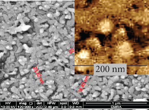
The morphological analyses of P3MA, PbS, and P3MA/PbS-QD structured thin films are shown in Figure 2. P3MA (Figure 2(a)) has a nanopore network consisting of nanoparticle agglomerates. The inserted figure shows a highly homogenous and porous structure. This structure is the key of the composite formation, in which the additional materials can penetrate or lodge inside the frame and form a high compact nanocomposite. Likewise, Figure 2(b) shows that the PbS-QD particles have a spherical shape inside and outside the P3MA network with increasing white color. These spherical shapes increase with increasing the Pb2+ concentrations from 0.01 to 0.07 M, as shown in Figures 2(b)–2(e), respectively. Moreover, Figure 2(f) shows the SEM image of the porous PbS-QD particle agglomerate, forming a nanostructure. This behavior is matched well with the previous literature [25–27].

The SEM image of (a) P3MA, (b–e) P3MA/PbS-QD composite with different Pb2+ ion concentrations of 0.01, 0.03, 0.05, and 0.07 M, respectively, and (f) PbS-QD/nanoparticles.


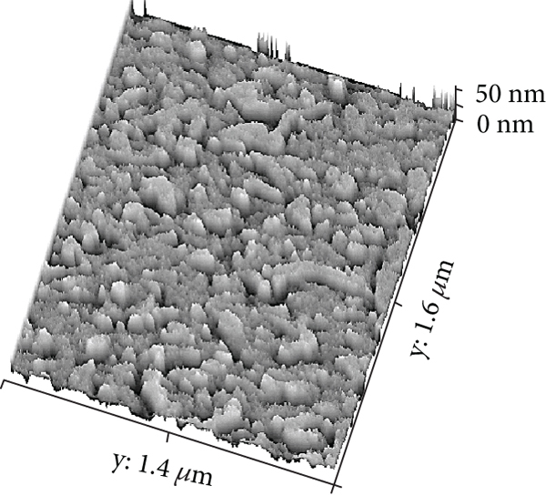
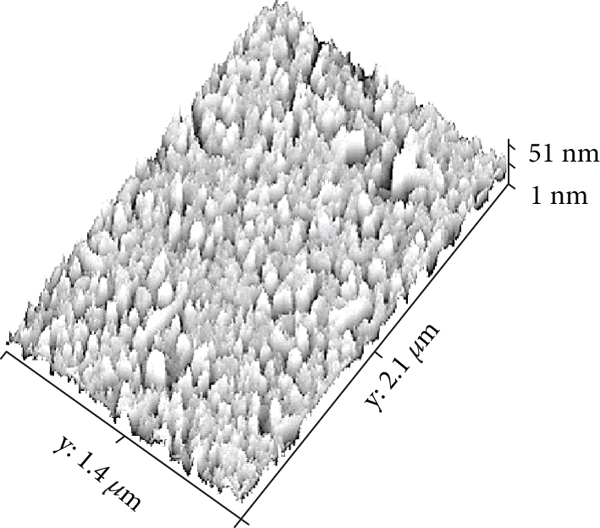
ImageJ software was used to determine the cross-section and morphology with high clarity to confirm the morphological structures of the prepared materials. Figure 3(a) shows the high porosity of the P3MA network, which acts as the site to receive the PbS-QD particles as seen in Figures 3(b)–3(e) with the different Pb2+ concentrations. The spherical white shapes increase with increasing the Pb2+ concentrations and accumulate on the surface and inside the porous network. Furthermore, Figure 3(f) shows the PbS cross-section and morphology, in which the porous structure appears clearly with QD particle agglomerates.

The cross-section and morphology of (a) P3MA, (b–e) P3MA/PbS-QD composite in different Pb2+ ion concentrations of 0.01, 0.03, 0.05, and 0.07 M, respectively, and (f) PbS-QD/nanoparticles.


These morphological properties of the P3MA/PbS composite were expected to have a high-efficiency optical absorption behavior, solely collecting each QD particle’s properties.
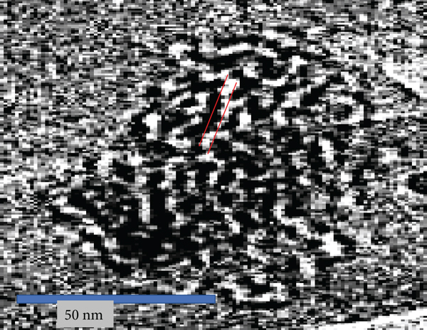
Based on the encouraging specifications seen in composite III, the TEM image of the latter is presented in Figures 4(a) and 4(b) using different magnifications. It shows that the composite was formed with high symmetry, and the PbS and P3MA are well embedded in each other. Figure 4(b) shows the actual particle sizes of the composite with an average size of 5 nm. Moreover, the interatomic distances for P3MA are about 0.4 nm. These morphological properties confirm the ability of the composite to be applied as an optoelectronic material with high optical absorption behavior related to the high P3MA and PbS-QD material junctions.

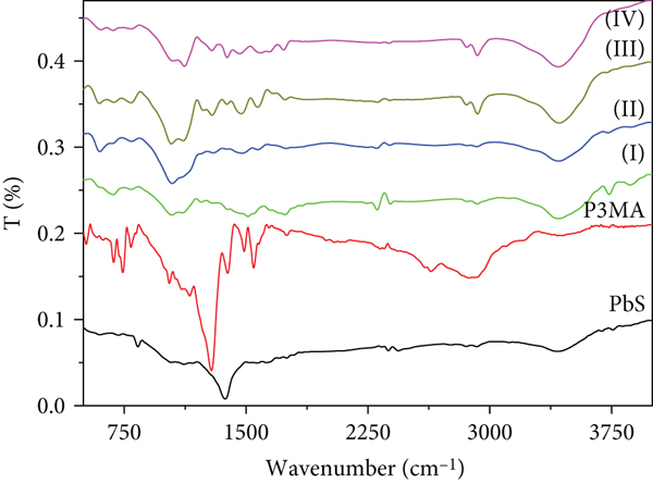
(a and b) TEM of composite III under different scale pares. (c) The XRD, (d) FTIR, (e) optical absorbance, and (f) band gap for P3MA, PbS, and P3MA/PbS-QD composites I, II, III, and IV under different Pb2+ concentrations.


Subsequently, the phase structure and particle sizes of P3MA, PbS, and P3MA/PbS-QD composites I, II, III, and IV were confirmed using the XRD analyses as shown in Figure 4(c). The P3MA XRD structure (red curve) includes one peak at
The chemical structures of the prepared P3MA, PbS, and P3MA/PbS-QD composites were examined by FTIR, as shown in Figure 4(d). The band positions for all P3MA, PbS, and P3MA/PbS-QD composites are summarized in Table 1. The PbS functional groups appear clearly in this figure (black line), in which the vibration of heteropolar PbS diatomic molecules appears at 1400 and 1061 cm-1. On the other hand, the stretching vibration of N-H, C-H, and C–N groups appears at 3401, 2918, and 1105 cm-1, respectively, corresponding to the P3MA functional groups (red line). In contrast, the C=C benzenoid and quinoid ring bands appear at 1301 and 1467 cm-1, respectively. The FTIR curves of P3MA/PbS-synthesized QD composites I, II, III, and IV with various Pb2+ concentrations 0.01, 0.03, 0.05, and 0.07 M, respectively, are shown in Figure 4(d). The functional groups of these composites are similar to those exhibited by both P3MA and PbS, with different shifts in band positions. After the composite formation, the N-H, C=C quinoid, and C–N vibrations shifted to average band positions 3424, 1470, and 1105 cm-1, respectively. Moreover, the vibration of the C=C benzenoid ring shifted to 1291 cm-1. We can conclude that composite III has the optimum band area based on these data.
A summary of the FTIR band positions for P3MA, PbS, and P3MA/PbS.
The optical analyses are essential to confirm the possibility of the prepared materials to be applied as optoelectronic materials. Figure 4(e) shows the absorption spectra of the P3MA, PbS, and P3MA/PbS-QD composites I, II, III, and IV. The absorption spectrum of P3MA reveals three absorption peaks at 304, 430, and 820 nm in the UV, Vis, and NIR regions, respectively. These peaks resulted from the Π-Π
The absorption coefficient (
The band gap of the P3MA/PbS composites was calculated through the Tauc equation below [30].
The band gaps for P3MA, PbS, and P3MA/PbS composites I, II, III, and IV nanomaterials are revealed in Figure 4(f) with values of 2.58, 1.1, 1.53, 1.52, 1.50, and 1.51 eV, respectively. This band gap of PbS-QD particles (1.1 eV) matches well its preparation size (5 nm), as mentioned in other studies in the literature [31–33]. Based on these values, composite III has the optimum band gap, close to the optimum band gap of 1.2 to 1.3 eV [34], which qualifies this material to be a highly efficient optoelectronic photodetector for light detection in UV, Vis, and NIR regions.
3.2. The Photodetector Electrochemical Study
3.2.1. Effect of Various Monochromatic Light
The response of the prepared photodetector, glass/P3MA/PbS (composite III), at various wavelengths from 390 to 636 nm is shown in Figure 5(a). From this figure, the produced current density in the dark (

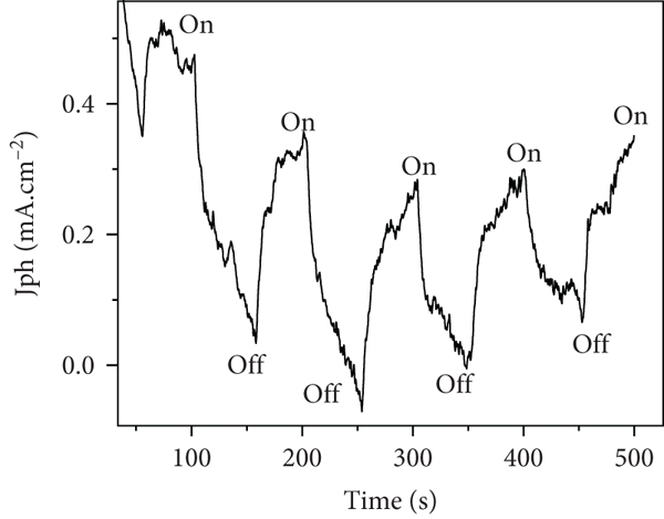
(a) The influence of dark and light wavelengths, (b) current density at 1.0 V, and (c) on/off chopped current for glass/P3MA/PbS photodetector at 25°C.

Moreover, the produced
Based on the
The high P3MA porosity surface and the PbS-QD particles’ active sites led to the high
Consequently, the prepared glass/P3MA/PbS photodetector has a high advantage in light sensing and detection in wide UV, Vis, and NIR regions. Moreover, the device has economic benefits, including the low-cost and easy preparation, that qualify the photodetector for potential industrial applications.
The effect of on/off chopped light, at very low bias voltage, on the photodetector response is shown in Figure 5(c). The photodetector has high light sensitivity under on and off chopped light. The dark current (
3.2.2. Optoelectronic Device Efficiency
The glass/P3MA/PbS (composite III) photodetector responds and senses the photon flux efficiently. This can be determined by calculating both

(a)

The
This broad light response is related to a large number of active sites in P3MA/PbS-QD particles. The PbS particles represent the light spots that can detect and capture the light photons that cause electron resonance. This process transfers additional electrons from the P3MA to its surface to generate the
The electron transfer sequence is the photodetector’s operation in the abroad light region. This unique property makes the synthesized optoelectronic photodetector overcome the drawbacks of the previous literature studies (mentioned in the introduction section).
In addition, Table 2 includes a comparison of the
Comparison of the photoresponsivity of the synthesized glass/P3MA/PbS photodetector with previous works.
3.3. The Plausible Mechanism of the Light Sensing
The light sensing mechanism of the glass/P3MA/PbS optoelectronic device depends on the band energy theory (Figure 7(a)). The schematic structure of the composite is mentioned in Figure 7(b). The electrons liberated under the photon flux have two motions hole-electron transfer (charge transfer). This transfer is only related to the hot electrons passing from the valency band to the conducting band. The second process is the accumulations of the electrons on the lowest conducting band level material. Under the two processes of electron transfer and accumulation, the local electromagnetic field is established around the semiconductor materials in which the produced electrons can effectively produce

(a) The plausible mechanism of the glass/P3MA/PbS optoelectronic photodetector device and (b) the schematic diagram of the composite structure.

There is a great advantage for the P3MA/PbS composite, in which the band gap is 1.50 eV with a minimal depletion layer, and the electrons can be easily transferred from the P3MA to PbS. This electron transfer reflects the high value of 0.029 mA.cm-2 (Figure 5(a)). The absence of the depletion layer causes the continuous flow of free electrons from P3MA to PbS-QD particles [51]. The large surface area of PbS materials enhances the acceptance of electrons from P3MA material, in which all the active sites are ready for acceptance the electrons from P3MA. Therefore, the prepared optoelectronic device can be applied for light sensing and detecting in abroad light regions: UV, Vis, and NIR.
4. Conclusions
A novel polymer-based optoelectronic photodetector glass/P3MA/PbS was synthesized and assessed for light sensing and detection in UV, Vis, and NIR regions. This photodetector has
Footnotes
Data Availability
All the data are mentioned in the manuscript, and there is no supporting data.
Conflicts of Interest
The authors declare no conflict of interest.
Acknowledgments
This research was funded by the Deanship of Scientific Research at Jouf University, grant number DSR-2021-03-0320.