
Abstract
Wireless sensor network provides a good solution for the state monitoring of large-scale structures. Compared to traditional approaches, it can greatly reduce the amount of devices wiring and the weight of the monitoring system. However, research of aviation structure monitoring application based wireless sensor networks is still in the initiation of the exploration stage. In particular, the developed wireless strain sensor node of WSN cannot be used in aviation structure because of low precision and other problems. In this paper, a high-precision and multichannel wireless strain sensor node of WSN is designed in detail. The wireless strain sensor node is composed of power module, multichannel strain sensing acquisition module, data-processing module, and wireless communication module. In addition, its special design of encapsulation makes it shock-proof and possess anti-interference property. To verify the functionality of the designed wireless sensor node for structural strength testing capability, several evaluation experiments are completed on a test piece of real aircraft. The experimental results show that the developed system has good performance in monitoring structural strain.
1. Introduction
Structural health monitoring plays an important role in various fields such as buildings, long span bridge, and railway. In the aerial domain, even tiny structural damage may lead to unimaginable disaster. Thus, it is particularly important in monitoring aircraft structure. Traditionally, large numbers of wires are adopted in the structural health monitoring systems for aircraft structures to realize communication among sensors and centralized data-processing systems. These wires on specimen structures bring about high installation costs and inefficient maintenance. If there are lots of testing sensors in the monitoring systems, these wires can be cumbersome and time-consuming. Therefore, using wireless sensor network (WSN) in structural health monitoring systems brings about much convenience and many advantages of high efficiency, high precision, low cost, and so on [1–8].
In recent years, WSN has been applied in many engineering fields, ranging from national defense to traffic controls, structural health monitoring, medical treatment and sanitation, and disaster monitoring. Straser and Kiremidjian [9] were the first to describe algorithms for structural health monitoring using wireless sensors network. Yin and Zhong [10] proposed a method to monitor vibration of rotating machines in power station based on WSNs. Hou and Bergmann [11] described an effective wireless sensing system to judge equipment failure. Shi et al. [12] developed an intelligent monitoring system for aquaculture using wireless sensor network based on 2.4 GHz frequency band. López-Higuera et al. [13] developed a staircase of structural health monitoring, where the higher the level, the higher the complexity and functionality. Liu et al. [14] presented distributed sensing for high-quality structural health monitoring adopting WSNs. However, there has been rarely similar research related to WSN designed for aviation structure, especially the aircraft strength testing applications. Arms et al. [15–17] produced similar wireless sensor nodes to measure micro strain for strength testing, but they are not designed for aircraft structure specially and the precision, signal channel, and other performances cannot meet the requirements of aircraft strength testing applications.
To realize aircraft strength testing applications, this paper proposed an optimized wireless strain sensor node with higher precision, multiple channels, and programmable amplifying function, which support 28 V aircraft power supply simultaneously. The wireless strain sensor node is composed of multichannel strain sensing module, digital processing module, wireless communication module, and power module. Each of the modules is designed in detail including corresponding theory, schematic, and analysis of design. To verify the functionality of the designed wireless strain sensor node for aircraft strength testing applications, a multipoint distribution testing system is developed for static tests of a real aircraft structure and several experiments to prove anti-interference are designed. The experimental results prove the effectiveness and practicability of the wireless strain sensor node.
2. Analysis of Main Challenges of the Proposed System
This paper proposed a more efficient system to realize aircraft strength test. The WSN makes the strength test more convenient and time-saving compared to traditional strength test with wire. The specially designed 28 V power supply can be provided by the aviation power handily and the optimized design supports hundreds of nodes working simultaneously, which is available for large-scale structural strength testing. Compared to the previous research [17], it is an optimized system with the following advantages:
It supports 28 V aircraft power supply. Due to the system presented in this paper mainly being applied in the aircraft structure strength test, 28 V external power supply is easier to obtain as aviation power. Therefore, the wireless strain sensor node must be able to be supplied with 28 V power voltage directly. The accuracy of strain test is less than 0.2%. Structure strain changes under different testing loads are the main testing parameter in the fatigue and static tests. Because these testing results are used to evaluate the mechanical properties of the aircraft structure, the wireless strain sensor node should have sufficient precision for strain measurement. The maximum range of the strain test is −5000 με~5000 με, and the SPC (stored program control) is multistage adjustable. The purpose of aircraft structural strength test is to determine the structural stiffness, stability, and maximum load. Therefore, the measuring span of the designed node should be large enough. The multistage adjustable SPC expands the measuring range and raises the accuracy simultaneously. Each node contains at least four strain sensor channels. For large-scale specimens or full-scale testing, the number of testing sensors could reach several hundred; therefore, every sensor node should be designed with multisensor input channels to reduce the node number; thus, the total cost of the network is reduced. The interface of strain gauge should be simple and easy to use and support the communication standard IEEE 802.15.4 [18,19]. The integrated shell packaging design has antivibration and anti-interference property.
Those testing nodes are arranged on the plane when the plane is still in the airport before it takes off or after it lands to make structural inspection. So, the testing period is in a controlled, open environment, and there may be much electromagnetic interference from the cellphone, large power-consuming equipment, and so on, and the nodes may be arranged on vibratory airplane position; therefore, anti-EMI and shock-proof design is very important.
In addition, the node needs to meet the requirements of small size and low cost.
In response to these requirements, the hardware platform of the wireless strain sensor node designed in this paper consists of multichannel strain sensing module, digital processing module, wireless communication module, and power module. Figure1 shows the block diagram of the node. The multichannel strain sensing module is responsible for sensing, amplifying, and filtering the strain signal of the sensing structure. The analog signal is converted into digital signal in the digital processing module. The wireless communication module realizes data transmission with base station or relay node. The power module is used for providing energy for each part of the circuit nodes.

The overall design diagram of wireless strain sensor node.
3. Design of the Power Module in the Aircraft Application
Due to the system presented in this paper mainly being applied in the aircraft structure strength test, 28 V external power supply is easier to obtain as aviation power. Therefore, the wireless strain sensor node must be able to be supplied with 28 V power voltage directly. However, the core chips of the digital processing module and wireless communication module in the node are chosen as low cost and low power consumption chips with 3.3 V supply power. As a consequence, a power management solution to make sure the system works reliably and stably is needed.
Since the power management chip LDO is superior to other methods with low noise and high stability, it guarantees the strain measurement precision of the node. Therefore, the LDO chip is adopted to realize the voltage conversion. The multichannel strain sensing module, digital processing module, and wireless communication module draw 150 mA of current while working and the LDO chip transforms the 28 V supply voltage to 3 V. According to the working principle of LDO chip, 3.705 W heat energy will be produced in the LDO. As a result, heat dissipation of power needs to be considered in order to ensure the normal operation of the node. Because two cascaded LDO chips can reduce the requirement of heat-sinking capacity of each LDO chip, this paper adopted this method to complete voltage conversion.
By comparing the performance parameters, heat capacity, prices, and market supply volume of different LDO chips, the MC7809 of U.S. ON Company is finally chosen as the first-stage LDO chip and the REG102-3.3 of U.S. TI Company as the second-stage LDO chip. Figure2 shows the schematic circuit diagram of the power module.

The schematic circuit diagram of power module.
4. Design of High-Precision and Multichannel Strain Sensing Module
4.1. Selection of the Strain Bridge
As one kind of resistive sensor, strain gauge changes a little when it is in response to the change of structural strain. The corresponding resistance variation is usually less than 1% of the nominal resistance. Therefore, it is important to measure a slight variation accurately in the resistance when using the strain gauge.
As shown in Figure3, one way to measure resistance variation is to apply constant current on the strain gauge and measure the change of its output voltage value. Hence, resistance variation of strain gauge is indicated by change of voltage. It shows that a precision current source and a method of precise measurement of voltage are required.
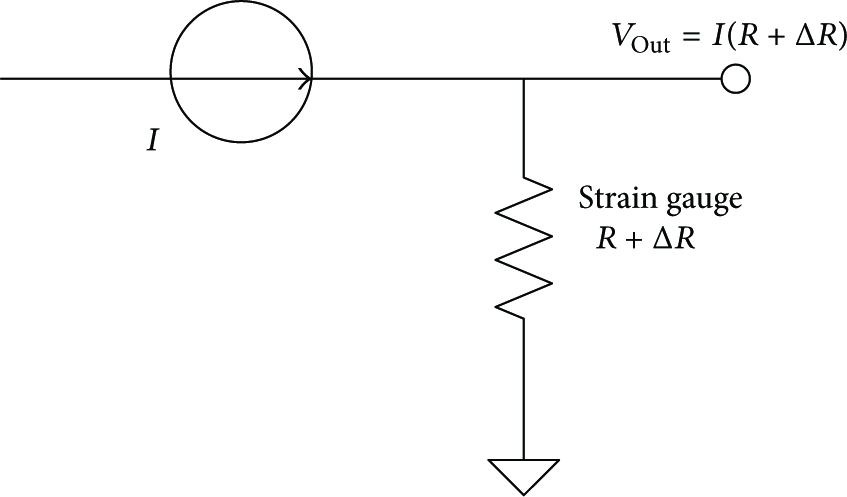
Use of constant current to measure resistance.
At the same time, the bridge provides a good way to measure tiny change of resistance accurately. Figure4 demonstrates a basic Wheatstone bridge. It is composed of four connected resistors, an excitation power supply

Wheatstone bridge.
In the application of the strain bridge, there may be a single gauge or two or four strain gauges. Figure5 shows four common strain bridges and the corresponding equations of the output voltage of bridge, excitation voltage, and resistance value of strain gauge.

Four common strain bridges and the corresponding output voltage of bridge.
As shown in Figure5, the resistance value of fixed resistances R and the nominal value of strain gauge are equal, while the strain gauge changes with
In summary, according to the analysis above and experience of the existing structure strength test, this paper adopted single strain gauge in the bridge in the wireless strain sensor node.
4.2. Design of Strain Sensor Conditioning Channel and the Ratiometric Technique
4.2.1. Design of Strain Sensor Conditioning Channel
The main purpose of the strain sensor conditioning channel is to amplify and filter the micro output signal of the strain bridge. Figure6 shows the typical diagram of the strain sensor conditioning channel.

The typical diagram of the strain sensor conditioning channel.
The purpose of the preamp is to amplify the tiny strain signal to make it suitable for A/D conversion. The low-pass filter is used to filter noise out, as there are various high-frequency electromagnetic noise and power-frequency noise in the test site and these noises will affect the accuracy of measurement. In addition, the second function of the filter is used as antialiasing filter. According to Nyquist sampling theorem, sampled signal must be bandwidth-limited before being transmitted into AD converter, and its highest frequency must not exceed half of the sampling frequency of ADC.
Particularly, the amplifier must be placed before the low-pass filter in the strain sensor conditioning channel. The RC active filter is adopted as the low-pass filter in order to reduce the volume of the node and resistance element is the main source of circuit noise. In consequence, if the amplifier is placed behind the filter, output SNR (Signal-to-Noise Ratio) of the node will be reduced [21].
4.2.2. The Ratiometric Method for High-Precision Measurement
Section4.1 indicates that measurement precision of strain bridge is less than accuracy of excitation voltage because the output signal of bridge is proportional to the excitation voltage. In the circuit design, the voltage references can provide reference voltage with 0.05% precision, such as ADR3433 of the ADI Company. However, the maximum output current is 10 mA and it cannot meet the requirements of the supply current in the strain bridge. The maximum output current of LDO power management chip is usually larger, such as REG102-3.3 of the U.S. TI Company with maximum output current of 250 mA, but its maximum precision of output voltage is limited. Therefore, LDO power management chip cannot meet the accuracy requirements designed in this paper obviously.
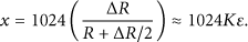
The ratiometric method provides a good solution to implement high-precision measurement of the strain bridge. The schematic diagram of ratiometric technique is indicated in Figure7. Formulas (1) and (2) show the relationship of structural strain and output voltage of the bridge structure measured ratiometric technique. Assume that the resolution of ADC is 12, the digital output voltage of ADC is x, and K is the sensitivity ratio of strain gauge. Hence,


The schematic diagram of ratiometric method.
As shown in Figure7 and formula (2), the output digital voltage of the ADC has nothing to do with the excitation voltage of the bridge finally by adopting the ratiometric technique.
4.3. Driver of the Strain Bridge and the “Three-Wire” Connection Method
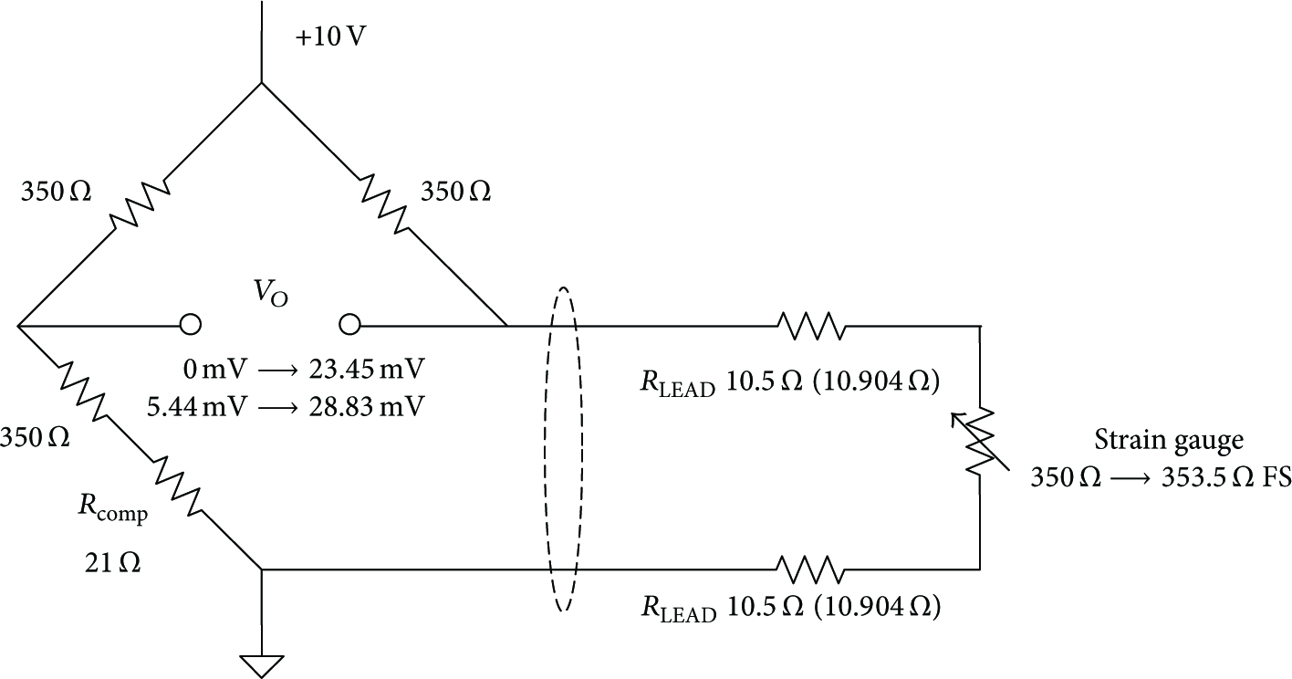
Although the wireless strain sensor node is disposed near the measured structure in the strength test, the wiring resistance in the strain gauge exists inevitably. The wiring resistance and its appendant noise are a key problem in strain bridge application. As shown in Figure8 of “two-wire” bridge, a 350 Ω strain gauge is connected to other parts of the strain bridge by twisted-pair copper wire of 1000 ft (1 ft = 0.3048 m). The resistance of the wire is 0.105 Ω/ft at 25°C. Therefore, resistance of the twisted-pair copper wire is 21 Ω. The temperature coefficient of the copper wire is 0.385%/°C. Gain of the bridge and the offset error can be calculated when the temperature increases by 10°C (as shown in Figure8, the value in bracket is the actual value of corresponding parameters at 35°C).
The error analysis of wire resistance in “two-wire” strain bridge.
As shown in Figure8, the 21 Ω resistance
If the full-scale variation of the strain gauge resistance with nominal resistance 350 Ω is 1% (3.5 Ω), the strain gauge resistance will be 353.5 Ω, which makes change of output voltage in bridge be ±23.45 mV.
When temperature increases to 35°C, variation of total wire resistance caused by change of temperature is 0.808 Ω (10.5 Ω × 0.00385 × 10°C × 2). Due to incremental wire resistance, the bridge will produce offset voltage of +5.44 mV with no change of strain and +28.83 mV offset voltage when full-scale strain change exists. Therefore, owing to the increased temperature, error of the offset voltage is +5.44 mV (+23% of full-scale output voltage), and the gain error is 28.83 mV − 5.44 mV − 23.45 mV = −0.06 mV (−0.26% of full-scale output voltage).
Figure9 indicates the “three-wire” bridge which can reduce impact on the output of the strain bridge produced by the wire resistance to the minimum. Assume that output voltage of the strain bridge is measured by a high-impedance resistance. As a result, there is no current in the guide line. When the strain resistance increases to full-scale value (353.5 Ω), variation of output voltage in the bridge is +24.15 mV.

The error analysis of wire resistance in “three-wire” strain bridge.
When the temperature increases to 35°C, the two
By comparison and analysis of the two bridges, it is easy to conclude that the three-wire system can reduce the measuring error well which is caused by the wire resistance of the bridge. In consequence, the “three-wire” strain bridge is adopted in the designed node in this paper.
4.4. Design of the Preamp Module
The maximum range of the multichannel strain sensing module designed in this paper requires to be −5000 με~5000 με and the multistage SPC (stored program control) is adjustable. In addition, the strain measuring accuracy needs to be less than 0.2%. When the bridge excitation voltage is 3.3 V, the fixed resistors and strain gauge are chosen to be 120 Ω, and the sensitivity coefficient of strain gauge is 2, the full-scale output voltage of the strain bridge will be 16.5 mV (−8.25 mV~8.25 mV). Such a small signal is easy to be covered up by electromagnetic noises. Therefore, in order to ensure the accuracy of the strain measurement, a precise preamplifier with low noise needs to be set after the output side of the bridge to realize output signal amplification. Meanwhile, after amplifying and filtering, the signal is converted to digital signal by the core chip of digital processing module, MSP430F1611. However, both the maximum reference voltage of the AD converter and the maximum input voltage of the sample conversion channel are 3.3 V. To make full use of range of AD converter and improve the measurement precision, amplification of the preamplifier is required to be program-controlled and adjustable.
Since integrated instrument amplifier is able to keep high accuracy of DC (direct-current) and high precision of gain in the noisy environment and condition of large common-mode signal, it is often used as preamplification of string-gauge bridge.
By comparison, AD8555 produced by the U.S. ADI Company is finally chosen. AD855 is a high-precision programmable instrumentation amplifier, including three programmable operational amplifiers and one output bias voltage DAC. It can set different magnification times and output bias voltage by different command word. Analysis of the importing error of AD8555 is as follows. Assume that value of strain gauge resistance is 120 Ω, its sensitivity is 2, excitation voltage of the bridge is 3.3 V, strain measurement range is −5000 με~5000 με, and the corresponding full-scale output voltage is 16.5 mV. Figure10 indicates the connection of bridge and instrumentation amplifier:
Offset voltage: Input offset current: Gain error: Nonlinearity of gain: Common-mode error: 0.1~10 Hz 1/f noise: All the error: 121 ppm + 1.5 ppm + 5000 ppm + 20 ppm + 180 ppm + 91 ppm = 5413.5 ppm. Resolution error: nonlinearity of gain +0.1~10 Hz 1/f noise = 20 ppm + 91 ppm = 121 ppm = 0.0121%.

Connection of the strain bridge and instrumentation amplifier.
From the analysis, a conclusion is obtained where AD8555 instrumentation amplifier is able to ensure that the wireless strain sensor node achieves goal of 0.2% measurement accuracy after calibration. Therefore, AD8555 is finally adopted as the preamplifier.
4.5. Design of the Low-Pass Filter
The second-order voltage-controlled voltage source low-pass filter circuit is selected as low-pass filter module. Figure11 shows the circuit diagram. As shown in the figure, it is made up of a second-order RC low-pass filtering circuit and a noninverting amplifier, and the voltage gain of noninverting amplifier is the passband voltage of low-pass filter. The low-pass filter is characterized by high input impedance, low output impedance, flat amplitude-frequency response curves in the passband, and rapidly declining amplitude-frequency response curves within the stop band.

The low-pass filter circuit of the second-order voltage-controlled voltage source.
Transfer function of the low-pass filter circuit is as follows:
The cut-off frequency of the low-pass filter is
5. Digital Processing, Wireless Communication, and Anti-EMI Packaging Module Design
5.1. Design of Digital Processing Module and Wireless Communication Module
In particular, the design of digital processing and wireless communication module takes the TelosB wireless sensor network node designed by University of California, Berkeley, as prototype in this paper. An MSP430F1611 microcontroller is adopted as core chip in the digital processing module and a CC2420RF chip is chosen in the wireless communication module as core [22]. The structure diagram is shown in Figure12.

The structure diagram of digital processing module and wireless communication module.
CC2420 is produced by Chipcon Company I2Co to realize ZigBee application as a RF transceiver. It has the characteristics of high integration, low voltage, low power consumption, and low cost. It supports the IEEE802.15.4/ZigBee protocol in the 2.4 GHz frequency band and is able to realize robust communication with data rate of 250 kbps [23]. The integrated DC voltage regulator in CC2420 converts the 2.1 V~3.8 V voltage to 1.8 V voltage. As a result, CC2420 can work normally without the extra voltage conversion circuit when extra voltage is 3.3 V.
The interface circuit of MPU and CC2420 is shown in Figure13. SFD, FIFO, FIFOP, and CAA in CC2420 are used as the indication of the wireless transceiver state of packet; the VRG_EN pin can control the DC voltage regulator in CC2420; the RESET is adopted to reset the CC2420. MSP430F1611 microcontroller sends commands to CC2420 and reads and writes the registers by SPI interface so that configuration of working state of CC2420 and data interchange is completed.

Interface circuit of CC2420 and MSP430F1611.
5.2. Packaging Design of Anti-EMI and Shock-Proof Integrated Shell
In order to make the WSN hardware systems lightweight and easy to be assembled and possess antivibration and anti-EMI property (electromagnetic interference), this paper designed shock-proof encapsulation for the WSN measurement in AST (aircraft strength testing) applications. Figure14(a) shows the encapsulation physical map. Figure14(b) shows the physical figure of one cross section of the designed encapsulation.

Design diagrams of anti-EMI and shock-proof integrated shell.
As shown in Figure14, the anti-EMI, shock-proof integrated shell includes several characters. Since the PCB board is fixed in the inner shell through a slot, the system is shock-proof, ensuring the hardware system is working normally in vibration. The design of all-metal package of the shell shields the electromagnetic interference effectively which guarantees the strain measurement precision. Metal grooves are advantageous to the heat dissipation of the node. Several mounting holes are designed to make the shell easy to be fixed. Besides, it is convenient to connect with external strain gauge with the specific strain interface board and the PCB is easy to assemble into the shell without connecting wire inside. What is more, all the packaging design makes the sensor node of small size and lightweight.
6. Performance Verification Experiments
6.1. The Calibration Test of the Multichannel Strain Sensing Module
In order to guarantee the effectiveness of the multichannel strain sensing module in application of structure strength test, a calibration test of the sensitivity, repeatability, hysteresis, and static error of multichannel strain sensing module is carried out.
There are many ways to calibrate the strain sensing channel; the method of parallel large resistance is used to calibrate the multichannel strain sensing module in this paper.
The strain bridge measures change of strain gauge resistance, while change of the strain gauge resistance is proportional to the structural strain. Therefore, if variation of a standard resistance is given, the strain sensing channel can be calibrated. This method can get high-precision rate of resistance change. As shown in Figure15 the five resistances are all precision resistance. Suppose that


Method of parallel large resistance in strain bridge calibration.
When calibrating the multichannel strain sensing module, the parallel large resistance is made up of several series resistors with different value in order to implement test of positive and negative stroke. In the positive stroke, resistances are short-circuited one by one by the wire, while, in the negative stroke, resistances are connected in the circuit one by one. Figure16 illustrates the operating diagram of the bridge calibration process.
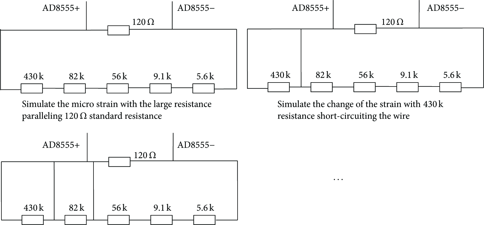
Operating diagram of the bridge calibration process.
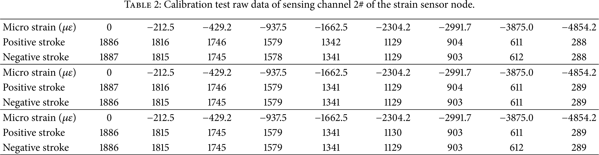
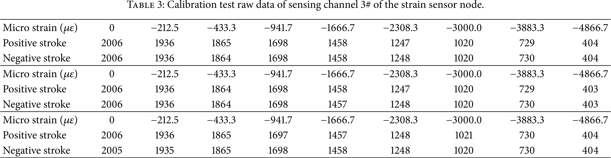
Tables1–4 show raw data of calibration of four strain sensing channels, and Figures17–20 indicate the positive and negative stroke curve of four sensing channels and their fitted curve.
Calibration test raw data of sensing channel 1# of the strain sensor node.

Calibration test raw data of sensing channel 2# of the strain sensor node.
Calibration test raw data of sensing channel 3# of the strain sensor node.
Calibration test raw data of sensing channel 4# of the strain sensor node.

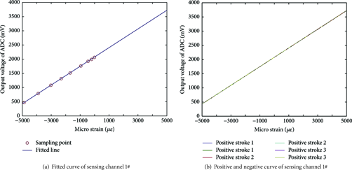
The calibrated result of sensing channel 1# of a wireless sensor node.
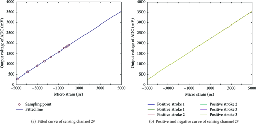
The calibrated result of sensing channel 2# of a wireless sensor node.
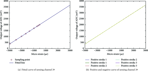
The calibrated result of sensing channel 3# of a wireless sensor node.

The calibrated result of sensing channel 4# of a wireless sensor node.
The main performance index of sensing channel 1# is as follows.
Repeatability. It is represented as

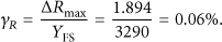
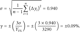
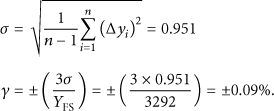
Hysteresis. It is represented as

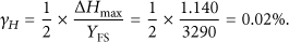
Static Error. It is represented as

Sensitivity. When digital output voltage changes to “1,” the corresponding micro strain variation is 3.04 με. This means sensitivity of the channel is 3.04 με per one digital voltage change, and the theoretical sensitivity is 3.05 με per 1 digital voltage change.
The main performance index of sensing channel 2# is as follows.
Repeatability. It is represented as
Hysteresis. It is represented as
Static Error. It is represented as

Sensitivity. When digital output voltage changes to “1,” the corresponding micro strain variation is 3.04 με. This means sensitivity of the channel is 3.04 με per one digital voltage change, and the theoretical sensitivity is 3.05 με per 1 digital voltage change.
The main performance index of sensing channel 3# is as follows.
Repeatability. It is represented as

Hysteresis. It is represented as

Static Error. It is represented as
Sensitivity. When digital output voltage changes to “1,” the corresponding micro strain variation is 3.04 με. This means sensitivity of the channel is 3.04 με per one digital voltage change, and the theoretical sensitivity is 3.05 με per 1 digital voltage change.
The main performance index of sensing channel 4# is as follows.
Repeatability. It is represented as

Hysteresis. It is represented as

Static Error. It is represented as
Sensitivity. When digital output voltage changes to “1,” the corresponding micro strain variation is 3.04 με. This means sensitivity of the channel is 3.04 με per one digital voltage change, and the theoretical sensitivity is 3.05 με per 1 digital voltage change.
6.2. Static Strength Test Verification
In order to validate the capability of the designed wireless strain sensor node based AST systems, in this paper, a multipoint system is developed for a test specimen of a real aircraft structure for static testing in Xian Aircraft Strength & Research Institute of China.
6.2.1. Experimental Arrangement
Test specimen used in the static strength is YL12 aluminum plate with size of 300 mm ∗ 200 mm ∗ 2 mm (length ∗ width ∗ thickness). As shown in Figure21, 72 strain gauges are pasted equally on the positive and negative sides of test specimen, with numbers 1~36 (negative side) and 101~136 (positive side), respectively. The “three-line” wiring method is adopted to connect the strain gauges and the external testing system.

Arrangement of 72 strain gauges on test specimen.
As shown in Figure22, the test specimen is clamped in a stretcher. The 36 strain gauges on negative side are connected with traditional strain measuring system (this system is regarded as a comparative system) while the other 36 strain gauges are connected to the wireless strain sensor nodes.
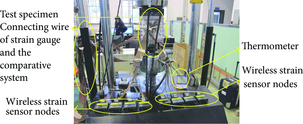
Physical map of arrangement.
6.2.2. Experimental Process
Firstly, dead load of 0.01 KN was preloaded to the test specimen and its strain value was regarded as null point of the two systems.
Then, dead loads of 1.4 KN, 14 KN, 28 KN, 42 KN, 56 KN, and 70 KN were loaded on the test specimen separately in the positive and negative stroke of static strength test. When the static load was increased to set value, all nodes collected data of strain 10 times and took their average as strain value under the corresponding load. Finally, repeat this process three times.
6.2.3. Comparison and Analysis
In the static strength test, data of the 36 strain gauges on the positive side are collected by the wireless strain sensor nodes designed in this paper. Choose test data of the four strain gauges 119, 120, 121, and 120 and data of 19, 20, 21, and 23 strain gauges in the comparative system for comparison. Figure24 indicates stress-strain curves of strain gauges 19/119, 20/120, 21/121, and 20/120 in three rounds of static strength test and the relation curve of average strain and its corresponding dead load.
By analyzing data in Figure23, the measured deviation of the two systems under the same static load is calculated. Tables5–8 show the calculation results.
19/119 strain gauge under the same static load.

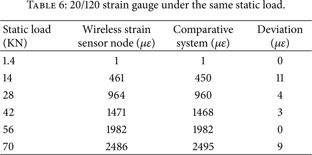
20/120 strain gauge under the same static load.
21/121 strain gauge under the same static load.

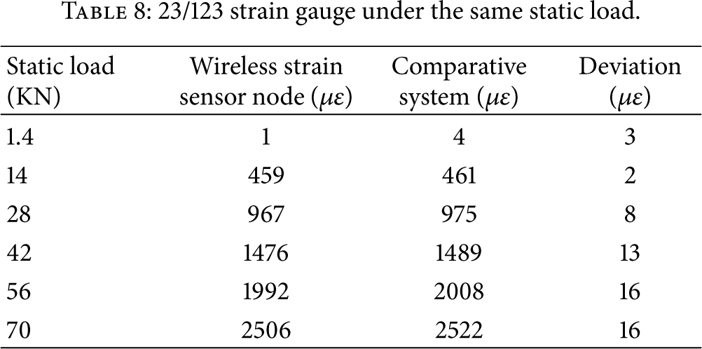
23/123 strain gauge under the same static load.

Contrastive results of the static strength test.

Arrangement of anti-EMI test.
By Tables5–8, it is concluded that the maximum deviation of strain measured by the two systems under each load is less than 25 με. This means that the wireless strain sensor node designed in this paper to test structure strength has good applicability.
6.3. Antijamming Experiment
6.3.1. Anti-EMI Experiment with High-Power Device
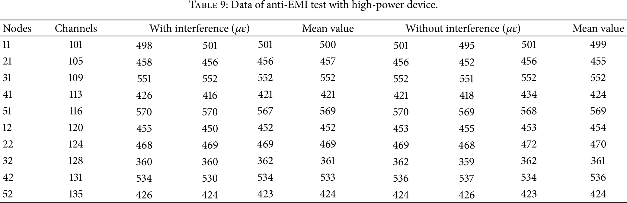
Anti-EMI experiment with high-power device is applied to verify ability of anti-interference of the wireless strain sensor node. During the test, the output signal of piezoelectric power amplifier based on PXI bus was connected to shell of the wireless strain sensor node directly. Then, start the power amplifier to simulate electromagnetic interference of high-power device. Anti-EMI test site is shown in Figure24. Test data is indicated in Table10. The basic unit in Table10 is με.
As shown in Table9, by comparing data under electromagnetic interference of high-power device with data without electromagnetic interference, it can be concluded that the electromagnetic interference of high-power device has no significant impact on the designed node. In summary, the wireless strain sensor node has the ability to cope with complex electromagnetic interference in engineering field.
Data of anti-EMI test with high-power device.
Data of anti-EMI test with radiofrequency equipment.

6.3.2. Anti-EMI Experiment with Radiofrequency Equipment
Anti-EMI experiment with radiofrequency equipment is used to prove the anti-interference ability of wireless communication of the wireless strain sensor node. In the experiment, a mobile phone in talk mode was placed near the node to simulate similar radiofrequency electromagnetic interference (2.4 GHz frequency band is used in wireless communication while 900 M/1800 MHz is adopted in mobile phone). Test data is shown in Table10. The basic unit in Table10 is με.
Table10 indicates that the radiofrequency interference has no obvious effect on the wireless communication of the wireless strain sensor node; no communication failure happened in the whole process.
7. Conclusions
A wireless strain sensor node hardware platform of WSN based aircraft strength testing system is presented in this paper. It is composed of multichannel strain sensing module, digital processing module, wireless communication module, and power module. Each of the modules is designed in detail, including the implementation method, circuit structure, and working principle. Finally, several tests to verify related performance of the designed node are carried out. The wireless strain sensor node is proved to be suitable for AST system with high-precision, multichannel, anti-interference, and shock-proof characteristics.
Footnotes
Competing Interests
The authors declare no competing interests.
Authors' Contributions
All authors have contributed to the presented work. Jian Wu and Xingmei Cui designed the whole system. Hongbing Sun and Yunpeng Xu conducted the implementation and wrote the paper. All authors have read and revised the paper.
Acknowledgments
This work is supported by the National Natural Science Foundation of China (Grants nos. 51105209, 61401211, and 51175267), Key University Science Research Project of Jiangsu Province, China (Grant no. 15KJA460004), Fundamental Research Funds for the Central Universities (Grant no. 30915118804), Jiangsu Province Science and Technology Support Program, China (Grant no. BE2012034), and Programme of Introducing Talents of Discipline to Universities (Grant no. B16025).