
Abstract
This paper proposes different low-level microarchitectural designs and frameworks for real-time monitoring and efficient control of on-chip sensor network for field programmable gate arrays (FPGAs). The main goals are to design low power, low-cost, and highly accurate monitoring and control mechanism using autonomous sensor agents and to dynamically reconfigure control of on-chip sensor networks by FPGAs. By collecting dynamic and real-time monitoring parameters such as voltage and temperature, the system becomes self-aware and is able to improve the utilization of FPGA resources and power consumption. The FPGA synthesis, place and route, and implementation were performed for the proposed design. The results after synthesis and implementation show a significant low usage of FPGA logic resources and efficient power consumption of all on-chip sensor components compared with previous approaches. Furthermore, the experimental results from the FPGA-measured on-chip sensor readings show high precision and accuracy in the measured voltage and temperature. Setting the dynamic reconfiguration refresh time at 1000 ms produces highly accurate FPGA-measured on-chip sensor readings compared with those at 100 and 500 ms. The proposed design technique and framework will assist network engineers and system designers by providing flexible and efficient real-time monitoring and control design of large and complex on-chip sensor networks and remote-sensing applications.
1. Introduction
The complexity imposed by on-chip sensor network monitoring and control increases with the scalability of the on-chip sensor network. Therefore, there is the need to have an intelligent and reliable low-level design of intelligent monitoring and control systems using autonomous sensor agents. Because different runtime physical parameters must be monitored, the need for accurate and efficient sensor communication mechanisms is very essential to ensure reliable monitoring and control of complex on-chip sensor network environment. This process also entails the design of low power and high-speed circuits for efficient and reliable network monitoring and control. The use of field programmable gate arrays (FPGAs) for autonomous sensor network monitoring and control is an interesting research domain in which low FPGA logic utilization, low power consumption, and accurate sensor readings are the major metrics for evaluation [1–5]. An autonomous sensor network is a special application for system monitoring, which is composed of several components such as a transducer, conditioning circuits, processing units, and data communication. The major functions of a sensor network are monitoring, collecting runtime ambient parameters, environmental adaptation, and making informed decisions about the observed control parameters [6–10].
As the flexibility and reliability of FPGAs increase, autonomous sensor agents can be embedded in FPGA to measure different runtime parameters. However, designing a sensor network on FPGA is a very difficult task to achieve in a short time because designers are limited to do beyond the FPGA manufacturer design specification. Similarly, the degree of complexity as well as sophistication of design automation contained in the FPGA makes it difficult for designers to tweak the FPGA circuitry to design and implement sensor networks [4, 5].
The on-chip sensor network runtime parameters such as voltage, current, and cross talk noise are used in controlling and monitoring information from the on-chip sensor network environment. Therefore, as the signals are transmitted within the logic blocks, they encounter delays. This delay component of the logic circuit should be minimized. Hence, the use of FPGA to implement sensor networks will be an efficient solution for a reliable on-chip sensor network packet transmission and retransmission scheme because logic and critical-path delays in FPGAs are minimal. Several methods to overcome these limitations include the use of feedback control system [5, 6, 11–14].
Chu et al. [1] proposed a multiplexing scheme that is simple enough to synchronize the sampling in a multichannel acquisition system with different sampling rates and many combined analog inputs as well as an improved sampling control to enhance system performance. FPGA was used in their design implementation. They used a sampling lookup table (LUT) to design a rule-based synchronous sampling frame to reduce the internal wiring and enhance resource utilization. The results of their experiments demonstrated the benefit of their approach. The proposed scheme can be employed in other related applications. Perera et al. [2] presented the design of low-cost, reconfigurable, and programmable smart sensor node using ZigBee. Their design was implemented using FPGA that incorporated the basic functionalities of the IEEE 1451 standard. The design of the sensor nodes comprised a processing unit and transducers with control capabilities in a single core to ensure reliable processing speed-up as a result of interprocess communication within a die. The experimental results on the basis of the measured pH value and temperature of water samples demonstrated the benefit of their approach.
Campos et al. [15] proposed a distributed autonomic inference machine. This machine could allow the sensor nodes to self-manage and to contextualize the tasks based on fuzzy logic. The results of their experiments demonstrated that the proposed machine is energy efficient by minimizing the number of messages to 48.8% and achieving 19.5% reduction in the energy consumed by the network. The review paper by Portocarrero et al. [16] provided an overview of the recent wireless sensor network (WSN) middleware systems that addressed the autonomic properties. Their aims were determining the best autonomic computing method that will provide a self-management feature of WSNs for middleware systems and studying the various interactions and behavior in WSN components. Their conclusions were summarized as follows: first, they addressed the major concerns about self-configuration, self-healing, self-optimization, and self-protection properties of the autonomous systems. Second, their investigation used diverse methods to manage the dynamic behavior of middleware systems for WSN, which included policy-based reasoning, context-based reasoning, feedback control loops, mobile agents, model transformations, and code generation. Finally, they identified the lack of complete system architecture design that provides full autonomy to the sensor network.
Designing an intelligent monitoring and control system requires the use of smart or intelligent and reliable sensors. The recent work by Echanobe et al. [3] has proposed a system-on-chip-based intelligent multiprocessor embedded system to control ambient environmental parameters. They achieved intelligent capability of their proposed approach by employing the concept of neurofuzzy system, which can reason and adapt to situational environmental changes. The authors Huijsing et al. [12] and Kirianaki et al. [17] proposed the concept of intelligent sensors. These are sensors with embedded intelligence and control system that can perform diverse functionality for environmental monitoring, self-adaptation, runtime observability, and network packet monitoring. Approaches to provide a smart interface for application-specific integrated circuits and FPGAs are provided by the authors of [18–25].
Other approaches to intelligent sensor system monitoring are presented in [26–29]. These approaches focused on the functionalities and communication protocols using transducers to make network communication possible. Ring and delay sensors have been used to study temperature and variations in FPGA [4, 5]. In Franco et al. [5], a ring oscillator was proposed to monitor the temperature in FPGA. This work considered a quadratic frequency in relation to a temperature sensor transfer function and examined how voltage variations affect the sensitivity of a sensor in relation to the number of stages in the oscillator. The authors found that, for larger oscillating chains, the voltage variations can be easily analyzed. Xi et al. [18] used ring oscillators to measure variability and temperature within the processor die. They also measured the power consumption when the system processor die is operating and idle.
The use of sensor networks to measure diverse runtime parameters like cross talk noise, on-chip interconnect temperature, switching activity, clock duty cycle, and other parameters is given in [26–32]. Petrescu et al. [30] proposed a signal integrity and efficient architecture to monitor diverse network-on-chip physical parameters, particularly temperature and voltage. Similarly, McGowen et al. [31] described the control system of a 90 nm Itanium processor, which utilizes on-chip sensors to measure power and temperature and modulates voltage and frequency to optimize the system performance. Sohn et al. [32] proposed a sensor-based solution for static random access memory to mitigate the uncertainties and fluctuation that exist among different device parameters. Their work shows that the information gathered by the on-chip sensors can be used to efficiently enhance reliability and performance of different functional system units.
A small number of methods have been proposed to collect useful information at runtime for on-chip sensor networks. For instance, Chan et al. [33] proposed an approach to use system management bus for communication among IP cores and a thermal-aware power management IP for low-level power management functions. Furthermore, Alexander et al. [26] proposed a hierarchical architecture to collect runtime parameters using network on-chip. Another approach was proposed by Ciordas et al. [27], which was a monitoring service framework, to support runtime observability of network-on-chip (NoC) behaviors, and application debugging was proposed.
As the complexity and scalability of on-chip sensor network continue to increase, a reliable and efficient low-level design that not only detects runtime ambient parameters but also offers better network performance, scalability, and flexibility of on-chip sensor network design using FPGAs is required. Hence, the use of FPGA for sensor network monitoring and control is very important. The authors in [34, 35] proposed a design of a web server for remote monitoring and control using FPGA. They provided a procedure for the implementation and application of their approach to remote monitoring of sensor networks on FPGA. Gomez Osuna et al. [35] proposed a monitoring infrastructure for FPGA self-awareness and dynamic adaptation. They employed sensor networks to provide dynamic adaptation and obtain data from the FPGA with reduced cost and easy implementation. They showed the significant benefit of their approach. Finally, the authors Kornaros and Pnevmatikatos [13] and García et al. [14] provided a detailed survey of the taxonomy of network-on-chip monitoring and control as well as FPGA-based design of sensor systems. However, the limitations of the previous approaches are as follows: (1) they did not provide real-time monitoring and a control mechanism for accurate measurement of the on-chip sensor network runtime parameters and (2) they did not provide efficient and convenient interface between the user and the FPGA to dynamically tune the operating ranges and reconfiguration refresh time to measure different on-chip sensor values.
In the current paper, we propose a low-level microarchitectural design infrastructure for real-time monitoring and control of on-chip sensor network-based systems for FPGA. We develop the design and implementation for efficient and reliable high-speed circuit technique of the on-chip sensor network runtime parameter monitoring and control, which use autonomous sensors that reside at the network interface (NI), to be dynamically configured and to communicate the runtime ambient parameters to the network monitor controller hardware. We provide detailed low-level design methodology and procedure and a user application for efficient and reliable on-chip sensor network monitoring and control for FPGAs. We also provide a webpage interface for the user to dynamically reconfigure the FPGA to conduct on-chip sensor readings and adjust the sensor ranges and reconfiguration refresh time. The proposed approach will provide engineers and system designers with a flexible and efficient real-time monitoring and control scheme for large and complex FPGA-based on-chip sensor networks. The prototype was implemented in FPGAs and the technology is applicable for ASIC as well.
The salient contributions of this work are as follows:
We propose a low-level microarchitectural design and infrastructure for real-time intelligent network monitoring and control for reconfigurable on-chip sensor network for FPGA. The intelligent sensor agents collect runtime ambient parameters such as voltage and temperature for efficient monitoring and control of on-chip sensor networks. We propose a real-time triggered protocol for efficient communication between the sensors and the monitoring and control unit. We provide a detailed low-level design procedure and implementation of the on-chip sensor network, sensor NI, and monitoring and control unit using both Synopsys and Xilinx design tools. We implemented the proposed design as a case study using Xilinx Vivado 2013.3 integrated design environment and Zynq 7000 FPGA device. The results after synthesis and implementation, including the device resource utilization, showed low FPGA logic resource consumption and efficient power utilization by the on-chip sensor components. We performed experiments using FPGA to measure and control the on-chip sensors. The experimental results from the FPGA-measured and controlled on-chip sensor readings show high precision and accuracy in the voltage and temperature readings. We found that setting the dynamic refresh time at 1000 ms produced accurate FPGA-measured on-chip sensor readings compared with those at 100 and 500 ms.
The rest of this paper is organized as follows: Section 2 presents the basic background; Section 3 discusses the design methodology; Section 4 discusses the simulation environment and simulation results; Section 5 presents the experimental setup, case study, and FPGA resource utilization and comparison with previous approaches; Section 6 presents the experimental results and discussions; and Section 7 provides the concluding remarks.
2. Background
The IEEE 1451 standard provides fast, efficient, and reliable means of converting transducer components into an intelligent sensor interface for efficient communication and transmission of sensor data to various NIs. A transducer is an electronic device that converts electrical signals from one form of energy to another. Therefore, a sensor is a special type of transducer that produces analog or digital electrical signals that represent the sensed physical, biological, or other environmental parameters. On the other hand, an actuator is a transducer that uses an electrical signal as an input and performs the required physical functionality [7–10].
An intelligent or smart sensor is a combination of both analog and digital transducer components, a central processing unit, and a network communication interface such as controller area network (CAN), interintegrated circuit (I2C), local interconnect network (LIN), and universal asynchronous receiver and transmitter (UART). It is also composed of hardware or software and conditioning circuits for sensor diagnostics and calibration, in addition to the communication mechanism and interface. Figure 1 shows the IEEE 1451 standard for a smart transducer interface (TI). The architecture comprises four subsystems: transducers consisting of sensors and actuators, signal conditioning circuit, data conversion subsystems, and application processor and network communication. The sensor output signal is conditioned by the conditioning circuit and is multiplied and converted into a digital signal using an analog-to-digital converter (ADC). The digital signal from the sensor is processed by a microprocessor with the help of a monitoring and control algorithm. The sensed parameters can be transmitted to the monitoring and control system using the network communication algorithm [7–9].

IEEE 1451 standard for smart TI [7].
As defined by the IEEE 1451 standard, a smart transducer is an intelligent system that provides enhanced capability beyond sensing and provides a mechanism for control of the sensed information. This feature provides a means of combining transducers for different applications in a controlled network environment with a high level of efficiency and reliability. Furthermore, the IEEE 1451 architecture provides functionalities such as self-diagnosis, self-description, self-identification, self-calibration, data processing, location awareness, and time awareness. The various components of the IEEE 1451 smart transducer architecture are shown in Figure 1. The network capable application processor (NCAP) subsystem provides the functionality for application processing and network communication mechanism between the sensors and actuators. The TI module subsystem is composed of a transducer signal conditioning and data conversion, which consists of a number of sensors and actuators. The TI provides communication methods and algorithms for efficient transmission of sensed data. Finally, the NI provides a means of communication between the NCAP and the outside devices or networks [7–10].
2.1. On-Chip Sensor Network Monitoring and Control System
The on-chip sensor environment is a very complex and dynamic system. Monitoring of the on-chip sensor as a dynamic system demands communication of the sensed data to a controller and the basic information regarding the controller input parameters to the actuators. Therefore, the structure, topology, switching, and arbitration of the on-chip sensor network solely depend on the monitoring, control, and communication mechanism or protocol used by the system. Hence, two major challenges need to be addressed: provision of efficient and reliable communication mechanism used by the network and provision of central and distributed control system that ensures real-time sensing, monitoring, and efficient processing of the on-chip sensory information. Therefore, an autonomous monitoring and control system for on-chip sensor network must consider the communication protocol and the constraints in relation to the clock time, network topology, switching, and arbitration [36–38].
On-chip sensor network monitoring and control can be regarded as a closed-loop system, which means that controllers are provided to connect to a feedback system, and sensors and actuators are installed to determine the overall function of the whole system. The on-chip sensor network must consider and address the following fundamental issues in a controlled loop system [20–25, 36–39]:
Suitability of the on-chip sensor network communication topology for a particular application. Addressing the constraints imposed by the communication mechanism, such as packet loss, network latency, delay, routing, and switching. Determining the monitoring and control goals that must be observed to facilitate proper coordination of each component in the whole network monitoring and control system.
To address these issues, there is the need to have an efficient and reliable monitoring and control infrastructure that will provide all the needed design methodology and framework to achieve the stated goals and objectives.
Figure 2 shows an intelligent monitoring and control system for on-chip sensor network using autonomous sensor agents. It shows the data transfer among different nodes in the system, that is, from the sensors to the controller and from the controller to the actuators. The on-chip sensor signal
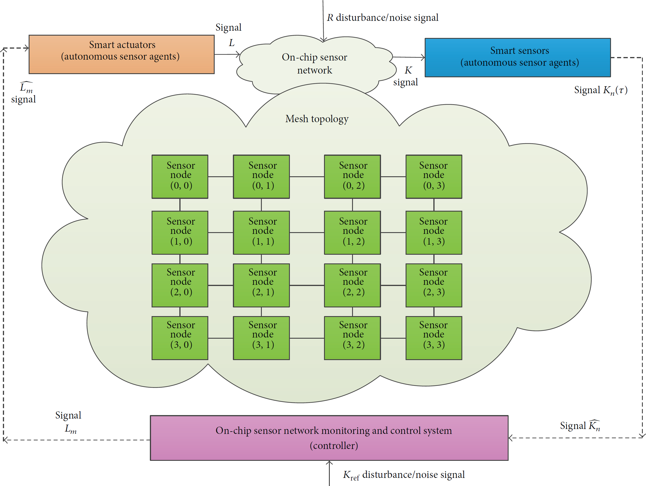
On-chip sensor network monitoring and control system using autonomous sensor agents.
3. Design Methodology
This section presents the design methodology of the proposed on-chip sensor network monitoring and control system with dynamic reconfigurable capabilities [26–49]. The proposed design detects runtime ambient parameters and communicates the sensed data to the monitoring and control hardware unit. Figure 3 shows the architectural design of the proposed monitoring and control system using autonomous sensor agents that reside in the NI to sense and report various parameter values to the hardware controller for onward analysis and processing. The architecture is a mesh network that is well suited for on-chip sensor die structure [13, 14, 47, 49]. It consists of 12 nodes (gateway) and IP cores. The NI provides a means of communication among the sensors and actuators, network nodes, and hardware monitor controllers. At each NI, three intelligent sensors are installed, namely, voltage, thermal, and temperature sensors. These sensors continuously sense and transmit the sensed data to the hardware controller that then processes the data and provides the necessary actions to keep the system in a smooth and healthy condition. The sensors communicate the sensed data via a standard protocol. This protocol is shown in Figure 4.

Proposed on-chip sensor network monitoring and control system using autonomous sensor agents on 4 × 3 mesh architecture.
Proposed real-time triggered on-chip sensor network communication protocol.
The temperature sensors measure the temperature variations to ensure that the system temperature does not exceed a certain threshold. The sensed data from the sensors are aggregated between four or more temperature sensors in different NIs. These temperature sensors form a cluster of sensors, and a cluster head (subcontroller) among them is set to collect and aggregate the sensed data from all sensors in the cluster and transmit them to the hardware monitoring and control system for further processing.
The thermal sensors measure the amount of heat dissipation resulting from the on-chip sensor cross talk noise and the data transmission and retransmission operations. For the thermal sensor operation, the procedure is similar to that of the temperature sensors where four or more thermal sensors form a cluster, and the cluster head (subcontroller) transmits the aggregated sensed data to the on-chip monitor controller hardware. The voltage sensors measure the voltage variations resulting from the current and resistance on the on-chip logic and the analog circuits. These sensors determine any transient and variation in the voltage drops across different components in the on-chip sensor network. Here, four or more voltage sensors in different NIs can form a cluster, and their sensed voltage input data are then combined for transmission to the monitoring and control unit. This process will ensure smooth and reliable monitoring and control of the entire on-chip sensor network [1–6, 11, 15–23].
Figure 3 shows that the intelligent monitoring and control system is composed of smart sensors and actuators that represent the autonomous agents, subcontrollers, main control unit, system monitor module, high-speed transceiver, and CAN controller. The monitoring and control system performs both central and distributed monitoring. Each sensor can communicate with its own cluster members and can perform data aggregation and forwarding to the main monitoring and control unit. Therefore, a distributed monitoring and control system is well established between the autonomous sensor agents and the main controller unit.
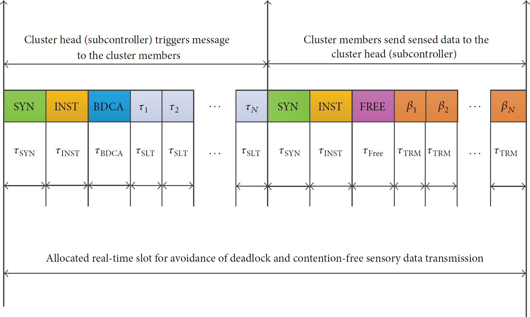
Figure 4 shows the real-time triggered protocol [6, 29, 48]. This protocol is deadlock and contention-free. The sensor nodes in each cluster are provided with real-time slots in which they receive sensed data from other nodes to communicate with the cluster head (subcontroller) or to transmit its own sensed data to the subcontroller. Communication among the sensors is synchronized in real-time to avoid delay and loss of sensor data. The subcontroller will trigger a message to all its cluster members to query if sensed data are available for transmission. The members will trigger a real-time message in form of response to the cluster if they have data to transmit, and a real-time frame will be allocated and synchronized in real-time for each member to avoid communication delays and loss of sensor information. The explanation of the variables used in the proposed protocol shown in Figure 4 is presented below:
SYN: it defines the real-time synchronization period between the cluster head (subcontroller) and cluster members. INST: it defines the real-time interval between the transmission and reception of the sensor data. BDCA: it determines the real-time in which sensory data are transmitted by the cluster head to the cluster members. FREE: it is defined as a real-time slot in which the cluster head (subcontroller) receives data from the cluster members; the cluster head uses the free slot in real-time to communicate with the on-chip monitor controller hardware on the status of the network.
3.1. On-Chip Sensor Network Monitoring and Controller Interface Design
Figure 5 shows the logic design of the main on-chip sensor network monitoring and controller unit. The design consists of several components that form the controller unit and interface to the different sensor networks. The main monitoring and controller design include the following: three bang-bang (on/off) controllers, a time domain system analyzer implemented as the main monitoring unit, 8:1 multiplexer (MUX) interface, ADC, smart sensors, actuators, a high-speed CAN transceiver, autonomous voltage sources, CAN engine controller, clock sources, and voltage-monitoring circuits.

On-chip sensor network monitoring and controller hardware interface design.
The reference voltage source supplies the required voltage to power the controllers and all the associated components of the monitoring and control system. The source is configured to generate different output sources such as a step and a periodic pulse. The initial pulse parameter and the amplitude values are set to 0.0 and 0.5 V, respectively. The 8:1 MUX interface provides the input from the output of the different sensors to the main controller system. It also acts as a conditioning circuit. Different sensor signals are conditioned (aggregated) to form a single strong analog signal, which is then amplified or buffered, as shown in the logic design. The use of a buffer is beneficial for interfacing with the sensors. It buffers the voltage to be fed into the ADC input. The output of the MUX is then fed into the ADC, which converts the analog signal into a digital form.
Two clock sources are connected to the ADC to provide a clocking mechanism for data conversion and transmission. The clock sources of the ADC are configured with the following settings: (on-time = 10.0 μs, off-time = 10.0 μs, initial time = 0 μs, and delay = 0.0 μs). Similarly, the clock source connected to the start pin of the ADC is configured with the following settings: on-time = 50 μs, off-time = 20 μs, initial time = 1 μs, and delay = 1 μs. These parameter values can be tuned to control both the input and output of the ADC. The output of the ADC is fed into AMIS-3660 high-speed CAN transceiver, which serves as an interface between the ADC and the CAN engine. The eoc pin of the ADC is connected to s pin of the CAN transceiver. The 8-bit digital output of the ADC is connected to the receiver (Rxd) input of the CAN controller. The Vcc input is connected to the Vcc source, and the ground pin is connected to the earth (ground). The transmitter (Tx) pin of the CAN transceiver is connected to the Tx pin of the CAN engine. The receiver (Rx) pin of the transceiver is connected to the Rx pin of the CAN engine, which provides a means of transmission and retransmission of sensor data and direct monitoring and control of sensor information [21, 40, 41, 50].
The CAN engine, together with the transceiver, provides a communication interface to the entire system and serves as NCAP, as defined by the IEEE 1451 smart TI standard [7–10]. The voltage-monitoring module block measures the voltages from the sensor input to the control unit. We set a limit for the upper and lower voltages. If the voltage falls below a certain level (0–5 V), it is reported to the control system, and appropriate actions are taken. Smart voltage transducers are attached to the controller input and output pins to monitor the variation in the input and output voltages from the sensors and actuators to observe and control the transmitted information.
The time domain system analyzer is the main monitoring interface that provides voltage analysis of the converted signals from sensor NI. The voltage can be swept within a given frequency range while performing both transient and time domain analysis of the monitored control system. The controller compares the converted digital input signals from the CAN transceiver and the output signal from the CAN engine. It then calculates the phase and gain responses of the voltage frequencies during the sweeping process. This information is fed into the simulator, and waveform plots of the signals are displayed in the waveform window of the simulator for further analysis. Figure 5 shows two actuators attached to the system analyzer input and output ports to measure the actual transmitted sensor signals. This process will ensure that exact sensory information is transmitted and received at both input and output of the monitored and control system.
The bang-bang (on/off) controllers were used to control and monitor the sensor information between the sensor interface and the main hardware controller unit. We set the positive_threshold voltage to 5.0 V and the constant_output_value to 1.0 V in order to control the output voltages from the sensors, actuators, and main control unit [40–44]. The pseudocode for the bang-bang controller is shown in Pseudocode 1.
( ( ( ( ( ( ( ( ( ( ( ( ( ( ( ( (
3.2. On-Chip Temperature Sensor NI Design
Figure 6 shows the on-chip temperature sensor NI design. The design consists of several components: an autonomous temperature source, four smart transducers (temperature sensors), four smart TIs to the temperature sensors, four operational amplifiers, 4-1 MUX, ADC, and two clock sources.

On-chip temperature sensor NI design.
The temperature source is the main source of thermal energy for the sensors and the TI, which generates a temperature difference across its input ports in a form of a pulse or a pulse train. The generated temperature is not related to the amount of heat that flows through the source, but it depends on the differential voltage across the input terminals of the source. Furthermore, the positive polarity of the source defines the temperature differential between the highest


The output of the 4-1 MUX (y) is used as an input to the ADC. The ADC converts the analog sensor data into a digital form. However, the output (y) from the 4-1 MUX can be sent to the main controller representing one cluster of the four sensors' data. In this case, the conversion from analog to digital is performed by the ADC on the main monitor controller unit. To ensure timely and accurate data conversion by the sensors, two clock sources are connected to the start and clock pins of the ADC. The clk1 source is configured with the following parameter configurations: on-time = 10.0 μs, off-time = 10.0 μs, initial time = 0.0 μs, and delay = 0.0 μs. The start clock source is configured with the following settings: on-time = 50 μs, off-time = 20 μs, initial time = 1 μs, and delay = 1 μs.
3.3. On-Chip Voltage Sensor NI Design
Figure 7 shows the design of a voltage sensor NI. The design consists of autonomous voltage source, smart voltage sensors, four TIs, four operational amplifiers, one MUX, ADC, and two clock sources. The autonomous voltage source is used as the main source for power supply to the voltage sensors and TIs. The two parameters of the voltage source are configured to supply continuous voltage to all the components in the system. The values of the parameters are as follows: initial voltage = 0.0 V and amplitude = 5.0 V. The characteristic equations for the voltage sensors (voltage to control interface) and the TI (control to voltage) are similar to (1)–(3). The output of the TI is fed to the operational amplifiers, which is then amplified and sent to

On-chip voltage sensor NI design.
3.4. On-Chip Thermal Sensor NI Design
Figure 8 shows the smart thermal sensor NI of the main controller unit. The interface consists of several components similar to the two interfaces for the temperature and voltage sensors described in Sections 3.2 and 3.3. A thermal power source is used to power-on the four sensors and the TI. The two parameters for the thermal power source are configured with the following settings: amplitude = 5.0 V and frequency = 25 Hz. The source generates a sinusoidal heat at its input ports. The thermal sensors (thermal to power control) sense and transmit the sensor data to the smart TI. The characteristic equation for the thermal sensor model is expressed as


On-chip thermal sensor NI design.
4. Simulation Environment
This section explains the detailed simulation procedure carried out to verify the proposed design. The design and implementation of the register transfer level (RTL) modules, models, and schematics of the proposed intelligent network monitoring and control system presented in Section 3 were performed using the Synopsys integrated design environment and tools [40, 41]. The Synopsys SaberRD provides hardware programming environment, design tools, and model libraries for designing low-cost and high-speed circuits and simulation environment. The tools are used to verify the functionality and efficiency of the circuit design under test. The different parameter values can be changed to verify the design functionality to ensure reliable and efficient network monitoring and control. We verified the functionality of the proposed design specification in the time domain using transient analysis to determine the variation in the sensor NI voltage signals and that in the monitoring and control unit over time. The simulation was run by setting the following parameter configurations:
Simulation time (end time) = 10,000 ms (10 s). Time step = 10 ns. Start time = default = 0 s. Threshold voltage = 0–5 V. ADC clock signal setting (on-time = 10 μs, off-time = 10 μs, initial time = 0 μs, and delay = 0 μs). ADC start signal setting (on-time = 50 μs, off-time = 20 μs, initial time = 1 μs, and delay = 1 μs).
The simulation time (end time) defines the time in which the simulator finishes the transient analysis. Meanwhile, the time step is the period in which the simulator finds an initial solution point during the simulation to project the next solution point in the simulation process. In addition to the end time of the simulation process, the simulator also outputs the execution time. Four RTL gate-level netlist files for the entire design are provided with a simulator during the compilation and simulation process. Three netlist files are provided: one for each NI and the other one for the monitoring and control unit. The simulation results in waveforms are shown in Figures 9 and 10.

Simulation waveforms for transient analysis of the variation in the reference voltage and the measured voltages over time for the (a) voltage, (b) thermal, and (c) temperature sensors.

Simulation waveforms of the transient analysis of the variation in the reference and measured voltages over time for the (a) analog and (b) digital signals.
4.1. Simulation Results
Here, we provide the simulation results in waveforms using the Synopsys integrated design environment and tools [40]. Figures 9 and 10 show the transient analysis results in the time domain of the variation in sensor voltages over time for the different parts of the monitoring and control unit.
Figures 9(a)–9(c) show the transient time domain analysis for the three on-chip sensor NI designs. Figure 9(a) shows the simulation results of the voltage sensor NI and the voltage signal variation at different time instances. We observed that the sensor signals are alternating with an amplitude of 0–5 V corresponding to the reference voltage of 5 V. The four sensor signals are combined (multiplexed and amplified) to form an aggregated signal. As expected, the aggregated sensor signals are measured to be 5.0 V, which shows a high accuracy in the measurement of the combined sensor signals with a very negligible error in the sensor measurement.
Figure 9(b) shows the variation in the sensor voltage at different time instances for the thermal sensor NI. As observed, no difference exists between the reference temperature source (voltage) and the measured voltage of the four aggregated sensors. As expected, the reference voltage and the measured sensor voltages are the same (i.e., 5.0 V), which shows accurate precision in the sensor measurement of the NI and the efficiency of the intelligent thermal sensor network design.
Figures 10(a) and 10(b) show the simulation results for the variation in the sensor signals (voltage) over time for the main monitoring and control unit. Figure 10(a) shows the measured analog signals at different time instances of the various components of the monitor controller unit compared with the input sensor measured signals from the sensor NIs. The figure shows that the bang-bang_1 output signal oscillates between 0 and 5 V (maximum), which indicates the same measured input sensor signals of 5 V.
The transceiver_txd signal remains stable and is measured to be 5 V at different time intervals. This indicates a continuous conversion of signals and a high accuracy in the sensor signal conversion from analog to digital by the ADC. The output signals for both the high-speed transceiver and the CAN controller engine are controlled and regulated by the bang-bang_2 and bang-bang_3 controllers. We can observe that the controlled voltage measurement of the bang-bang_2 controller is 5 V measured at different time intervals. The bang-bang_3 controller voltage connected to the system monitor unit to control the monitor input and output is also measured to be 5 V, which shows that the input sensor signal from the NI is well monitored and performs control without losing sensor precision and accuracy.
Figure 10(b) shows the digital signal output of the converted sensor signals by the monitoring and control unit. The different digital bits of the converted sensor analog signals are output through the digital bits (0–7) of the ADC output. The transceiver signal was observed to be stable and high at different time instances.
In conclusion, the simulation results verified the functionality of the various design components of the sensor NIs and the monitoring and control unit. The actual application of this proposed approach is implemented using FPGA as a case study. The details of the case study and FPGA implementation are presented in Section 5.
5. Experimental Setup
This section explains the experimental procedure used to design, implement, and verify the proposed on-chip sensor network monitoring and control system using FPGA. To validate the proposed approach through a real-life scenario, we implemented a case study for on-chip sensor network monitoring and control using FPGA. We used the Xilinx Vivado 2013.3 integrated design environment and the Zynq 7000 XC7z020 CLG484-1 AP SoC FPGA device for synthesis, placement, routing, and implementation of the proposed system. Figure 11 shows the on-chip sensor network monitoring and control unit implemented using Xilinx ADC (XADC) and SYSMON IP cores [43, 44]. The XADC and SYSMON IP cores provide an interface for designing on-chip sensors and user-defined external sensors to the main monitoring and control unit. The system provides capabilities for self-awareness and adaptation to dynamically tune the different parameter values at runtime to measure ambient parameters such as temperature, voltage, and thermal energy variations. It is based on a highly precise analog measurement system consisting of a 12-bit ADC and other circuit elements. The ADC has a least significant bit with a size equivalent to 1 mV. Several input and output pins are provided to achieve high performance and accurate measurements from the on-chip sensors and the remote sensors connected to the system interface [26–35, 42–46].

Block design of on-chip sensor network monitoring and control system using XADC and SYSMON IP cores.
Six different sections are present in the monitoring and control unit, as shown in Figure 11. The dynamic reconfiguration ports (DRPs) allow the system to be reconfigured according to certain values of input and output signals to the monitoring and control unit. The control section pins provide three signals that enable the conversion of the sensor analog signals to digital signals. These are the reset, conversion, and clock signals. The input to these signals allows the sensor data to be converted to digital signals. In addition to the on-chip sensors, remote sensors can also be interfaced to the main controller unit via the auxiliary input; up to 16 remote analog inputs can be connected to the system.
The DRP, advanced extended interface (AXI4), AXI4-stream, and I2C interfaces provide a dedicated communication mechanism for the system to allow interfacing with remote devices (external sensors). The monitor and controller unit provides the necessary monitoring and control of the variations in temperature, heat, and voltage of the on-chip sensors. The system is also configured to generate an alarm when a threshold value is exceeded. Figure 12 shows the RTL netlist schematic after synthesis, placement, and routing of the implemented monitoring and control system on Zynq 7000 XC7z020 CLG484-1 FPGA board using the Xilinx Vivado 13.3 integrated design environment.
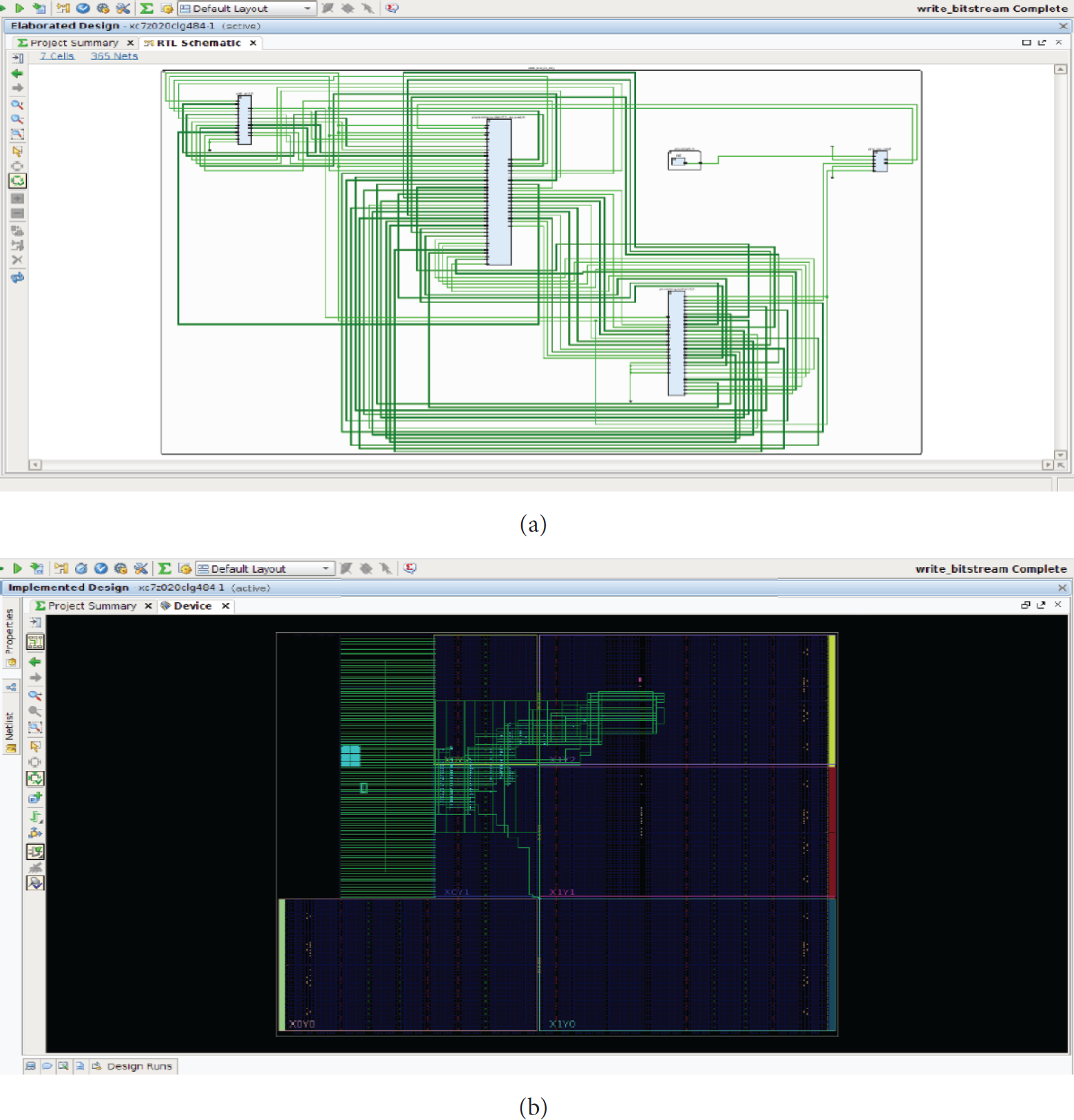
Illustration of the on-chip sensor network monitoring and control system. (a) RTL schematics. (b) Routing resources of the Zynq 7000 AP SoC FPGA device.
The architecture shown in Figure 11 consists of the XADC and SYSMON IP interface that are present in all Xilinx 7 series FPGA devices, including the Zynq 7000 families [43, 44]. The central processing unit is based on ARM Cortex-A9 processing system and is used to monitor and control the on-chip sensor variation in the measured temperature, voltage, and power supply. Similarly, the remote sensors connected to the main unit can also be monitored and controlled. Furthermore, the system will set an alarm when over temperature, over voltage, and under voltage, and so forth, occur. This feature will ensure smooth running and proper functioning of the whole system.
5.1. Case Study
This subsection provides the detailed explanation of the proposed case study using the Zynq 7000 FPGA board [43–47]. This case study uses a central processing unit (ARM Cortex-A9 core) to monitor and control the variation in temperature and voltage of the on-chip sensor and remote sensors connected to the FPGA fabric. The Xilinx Zynq 7000 is flexible and efficient architecture based on all programmable system-on-chip architecture. The device consists of a dual-core ARM Cortex-A9 MP Core processing system and enhanced Xilinx programmable logic in one integrated FPGA fabric. In the proposed design, the processing system is the main monitoring unit that provides basic functionalities with the Cortex-A9 MP Core central processing unit. The XADC acts as the control unit, which works together with the processing system. The other components installed in the processing system include the on-chip memory, on-chip sensors, input and output devices, auxiliary memory, and interface to the remote-sensing devices.
The monitoring and control system provides communication using different interfaces such as I2C, DRP, and JTAG. The control system uses another form of communication interface, which is the industrial input and output (IIO) framework-based Linux driver [44–46]. This driver works as a device driver for an application that uses a control system and the AXI and DRP communication interfaces. An interesting functionality of this driver is its ability to configure the control system to be used in different functionalities, for example, receiving data from the control system and providing information for different parameter states and configurations in the user space provided in the intended application. In this case study, we demonstrate how the IIO-based Linux driver is used for on-chip sensor network monitoring and control application. We show how the control system can be used to provide a hardware design in the programming logic, which creates a dedicated communication between the control and monitoring system using the DRP and AXI port communication interfaces. To make the application more user friendly, a web server-based design is provided for the user to interact with the monitoring and control system. The results of the dynamic monitoring and control system are displayed on a webpage for the users to see and change the configuration parameters to observe the variations in the measured on-chip temperature and voltage parameters, as shown in Figures 13 and 14.

On-chip sensor network monitoring and control system (hardware interface).
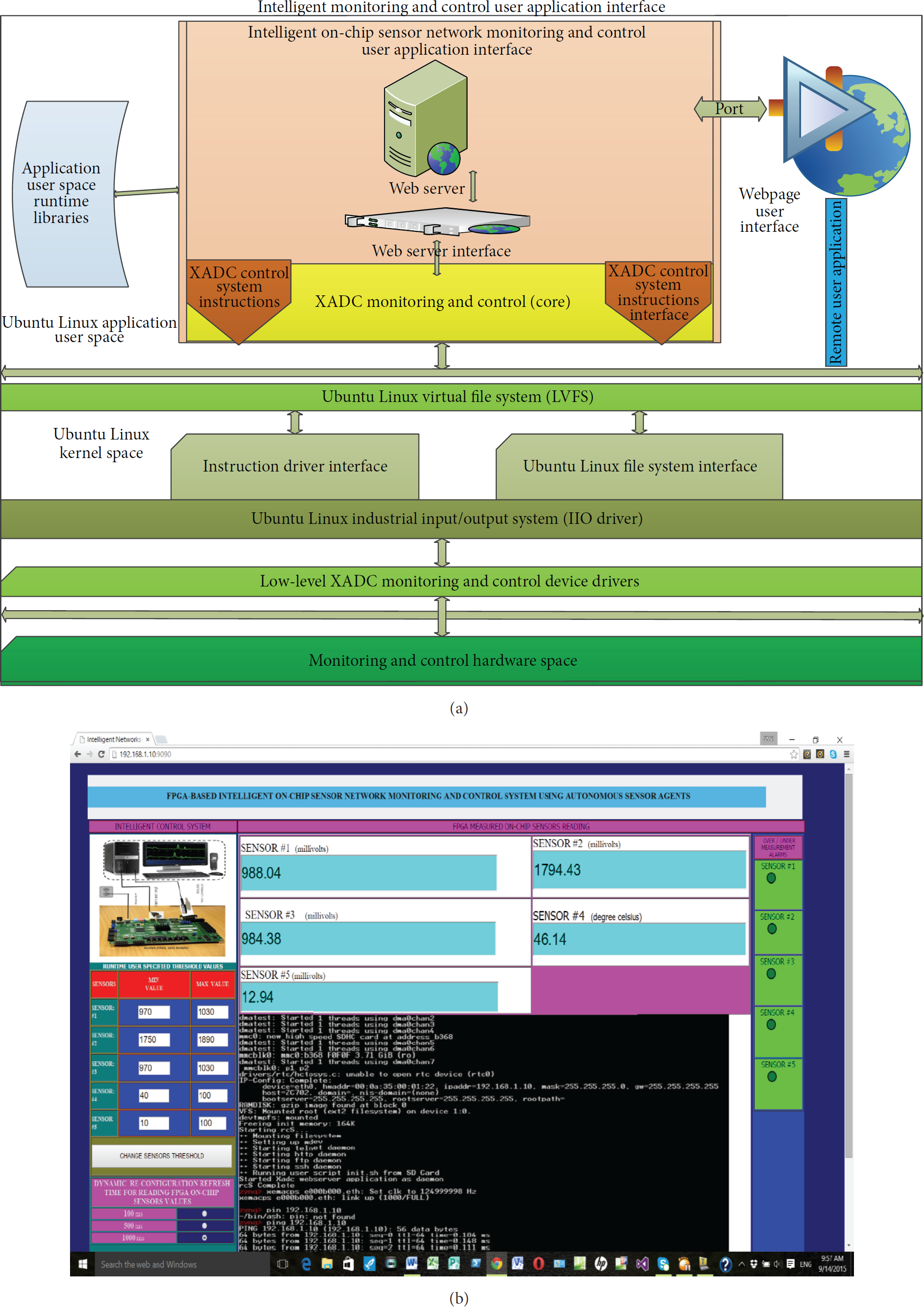
On-chip sensor network monitoring and control system. (a) User application interface design. (b) Webpage user interface.
The architecture of the hardware monitoring and control system as well as the connectivity between the control system in the programming logic and the processing system is shown in Figures 13 and 14. The DRP is used for reading and writing the sensor data into the control system DRP address register. The control system then translates the AXI4 transactions into the DRP address, which are used by the monitoring and control unit. An AXI interrupt controller is then instantiated, which translates the alarm output from the control system into various interrupt events for execution by the ARM core processing system. The control system interface to the monitoring system is set to control the user-specified configuration executed in the context of the user application layer. Here, an instruction can be issued through the instruction interface to read and write the sensor values. For instance, a 32-bit instruction next to a no-operation instruction is written to first-in-first-out (FIFO) buffers. These instructions are transmitted to the control system using the communication interfaces, that is, DRP and AXI4. In this manner, any word that moves into the instruction FIFO buffer moves a similar word into the data FIFO buffer. This scenario also applies to the DRP. As data are moved out of the instruction FIFO buffer, the old values stored in the control unit dynamic reconfiguration register also move out. At the end of the specified time interval, the result of the current DRP read operation will be output at the control unit register for further processing by the monitoring and control system [3–14, 17–20, 43–47].
The web server or user application in this case study employs the IIO framework device driver, as mentioned earlier. This is a standard means of providing support for ADCs. It provides two basic functionalities: file system interface for communication with various devices (sensors) connected to the system and character driver interface to receive event information from the subsystems to the user application space in the monitoring and control system [43–47]. The basic sections of the on-chip sensor network monitoring and control user application are briefly explained as follows:
On-chip sensor network monitoring and control: this subsystem provides a means of communication with the IIO system Linux device driver for functionalities like retrieving data from sensors, hardware configuration, synchronous/asynchronous event handling, and control mechanism. Web server subsystem: this subsystem of the monitoring and control unit addresses the connection request from remote web users. The users can acquire sensor data and other information through the web server interface. Sensory information and event notification and updates are provided to the server through the monitoring and control unit. Web interface subsystem: this subsystem provides the basic connection and interface for the web server and the monitoring and control system. The interface provides the functionality to set the threshold values of the different alarms and communicates these values to and from the web server interface for efficient monitoring and control. Web client subsystem: this subsystem provides functionality to users to tune the different parameter values of the temperature and voltage thresholds. The web client operates in a web browser and provides communication to the web server using a communication port. A graphical user interface is provided to obtain the sensed data from the sensors and the possibility of tuning the threshold values and dynamic reconfiguration refresh time. Figure 12 shows the implemented monitoring and control user application and web interfaces.
5.2. FPGA Resource Utilization
This subsection provides the results of the FPGA logic resource utilization of the postsynthesis and implementation (i.e., placement and routing) on the Xilinx Zynq evaluation kit ZC702 XC7Z020 CLG484-1, Zynq 7000 AP SoC FPGA device. Tables 1–4 list the resource usage at different design implementation stages. Tables 1 and 2 list the FPGA implementation results of the logic components for the on-chip sensor network monitoring and control system. We observe that the implemented design uses very small amounts of FPGA logic resources, that is, 2823 out of 482901, which is equivalent to 0.585%, compared with the results presented in [1–4, 23, 34, 35] as provided in Table 5. This result indicates low-cost utilization of the logic resources when implemented in a medium-sized seven-series FPGA device. This result validates our stated objective of achieving a low-cost intelligent monitoring and control system. After the design synthesis, we optimize the design using the Xilinx Vivado tool to efficiently route the design into the target architecture. In Table 2, we can observe that because of the optimization done to route the design, a slight reduction in the amount of logic consumption occurs. Table 3 lists the low-level primitives used by the implemented design and their utilization numbers.
FPGA postsynthesis (device placement) resource utilization implemented on Xilinx Zynq evaluation kit ZC702, XC7Z020 CLG484-1 Zynq 7000 AP SoC FPGA device.

FPGA postimplementation (device routing) resource utilization implemented on Xilinx Zynq evaluation kit ZC702, XC7Z020 CLG484-1 Zynq 7000 AP SoC FPGA device.

FPGA low-level primitive resource utilization implemented on Xilinx Zynq evaluation kit ZC702, XC7Z020 CLG484-1 Zynq 7000 AP SoC FPGA device.

FPGA on-chip sensor component after placement and routing power resource utilization implemented on Xilinx Zynq evaluation kit ZC702, XC7Z020 CLG484-1 Zynq 7000 AP SoC FPGA device.

FPGA resource utilization comparison with previous works.

%: percentage of logic resource utilization.
#: number of logic resource.
Not provided: the authors did not provide the power utilization result.
Table 4 lists the power distribution and utilization of the various on-chip sensor components after placement and routing. This distribution consisted of both dynamic and static power consumptions. We can see from the table that all on-chip sensor components show very low power consumption. We achieved 0.118 W (118 mW) of static power and 0.011 W (11 mW) of dynamic power consumption, a total of 0.129 W (129 mW), which represents a 2.26% of both dynamic and static power consumption, for all on-chip sensor components as compared with the results presented in [2, 3]. This result also agrees with our stated objective of achieving low power consumption in medium-sized seven-series FPGA device.
5.3. FPGA Resource Utilization Comparison with Previous Works
Table 5 shows the FPGA utilization results comparison with previous works [1–4, 23, 34, 35]. The comparison with the state of the art seems to be difficult due to the fact that there are a lot of differences in terms of the FPGA implementation architectures, sensors, and sensor networks and some of the proposed approaches did not provide FPGA power utilization result. Furthermore, the types of logic resources provided by the previous approaches are different from one implementation to another. However, the utilization results shown in Table 5 help to acknowledge the efficiency and flexibility of the proposed approach compared with the state of the art.
6. Experimental Results and Discussion
This section provides the results of the experiments to monitor and control the FPGA on-chip sensor readings. The essential metric for evaluating the FPGA on-chip sensor readings is its accuracy; that is, how accurate does the FPGA report the sensed on-chip voltage and temperature readings? Although the FPGA on-chip sensors are specified in terms of accuracy based on the manufacturer datasheet, the real significance is the on-chip sensor error. For instance, the temperature sensor specification for accuracy is ±4% full scale (FS) within the range −40°C to +100°C, which means that the on-chip sensor error will not exceed ±4% of its FS within its calibrated range. Therefore, the evaluation of the FPGA on-chip sensor accuracy represents the process of determining its maximum error [43, 44, 50].
We conducted several experiments using five different sensors, namely, Sensors #1–#5. Sensor #4 is a temperature sensor that measured the FPGA on-chip die temperature in degree Celsius and operates within a set threshold limit. The remaining four sensors are power sensors, which measure the on-chip voltage variations in millivolts within monitored and control threshold value. Tables 6–21 list the FPGA-measured on-chip sensor readings. Each table represents the four experiments we conducted, taking 10 readings in each experiment for a total of 40 measured readings from the FPGA on-chip sensors. The readings were averaged to remove the gross and systematic errors from the observed readings. The FS percentage error or accuracy was calculated for each observation and averaged across the 40 readings. We varied the dynamic reconfiguration refresh time to query the FPGA on-chip sensor readings from the webpage at 100, 500, and 1000 ms to determine the effect of the reconfiguration time with respect to the sensor accuracy. The details of the experimental results are presented in the next subsection.
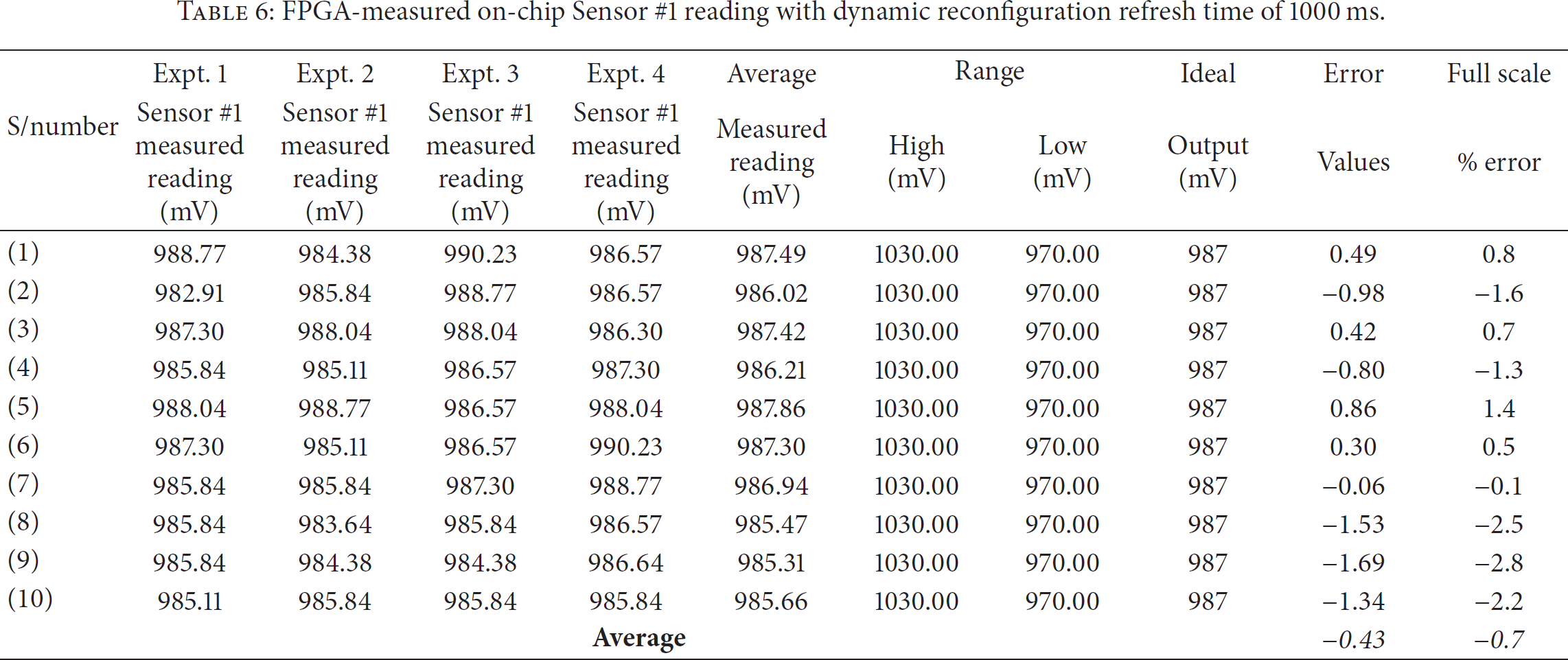
FPGA-measured on-chip Sensor #1 reading with dynamic reconfiguration refresh time of 1000 ms.
FPGA-measured on-chip Sensor #2 reading with dynamic reconfiguration refresh time of 1000 ms.

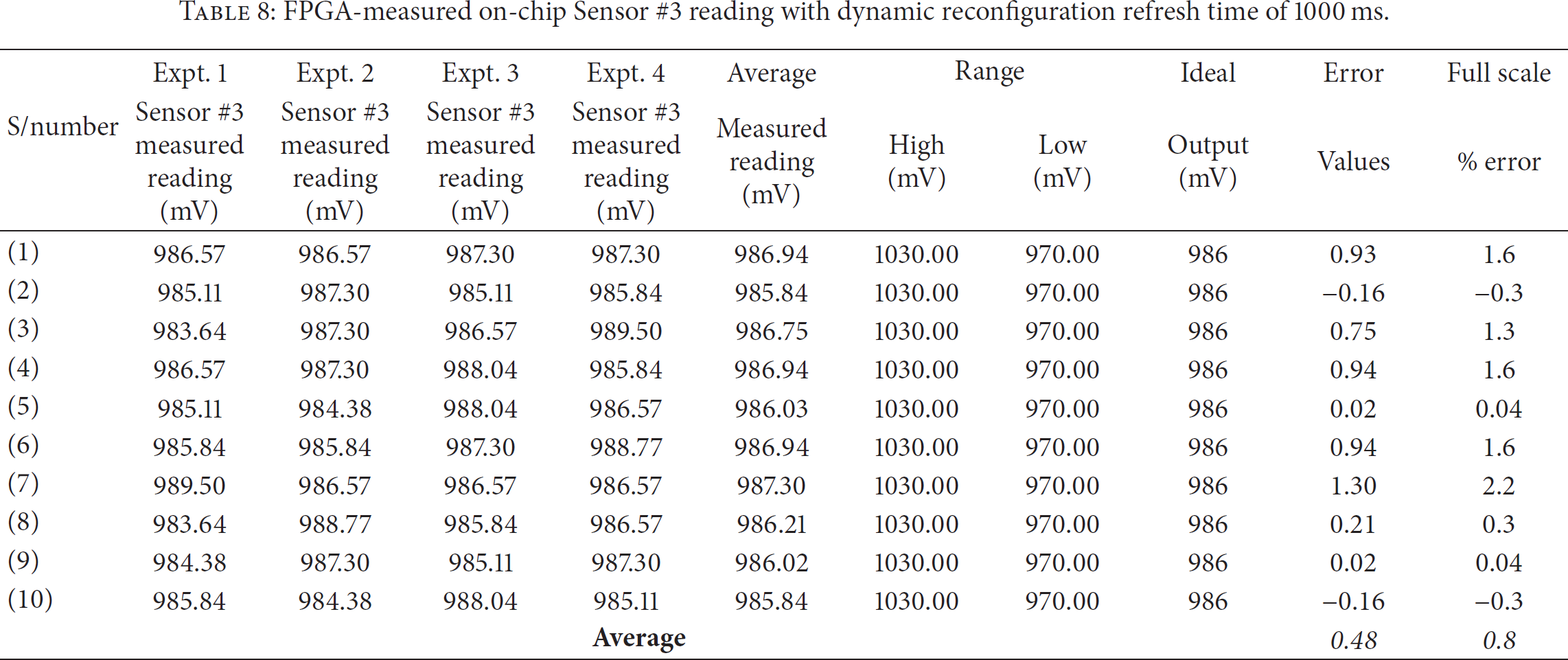
FPGA-measured on-chip Sensor #3 reading with dynamic reconfiguration refresh time of 1000 ms.
FPGA-measured on-chip Sensor #4 reading with dynamic reconfiguration refresh time of 1000 ms.

FPGA-measured on-chip Sensor #5 reading with dynamic reconfiguration refresh time of 1000 ms.

FPGA-measured on-chip Sensor #1 reading with dynamic reconfiguration refresh time of 500 ms.

FPGA-measured on-chip Sensor #2 reading with dynamic reconfiguration refresh time of 500 ms.

FPGA-measured on-chip Sensor #3 reading with dynamic reconfiguration refresh time of 500 ms.

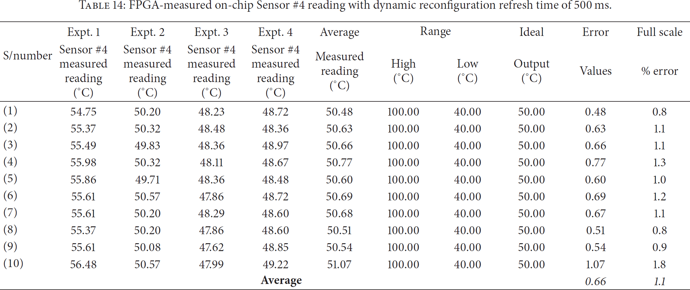
FPGA-measured on-chip Sensor #4 reading with dynamic reconfiguration refresh time of 500 ms.
FPGA-measured on-chip Sensor #5 reading with dynamic reconfiguration refresh time of 500 ms.

FPGA-measured on-chip Sensor #1 reading with dynamic reconfiguration refresh time of 100 ms.

FPGA-measured on-chip Sensor #2 reading with dynamic reconfiguration refresh time of 100 ms.

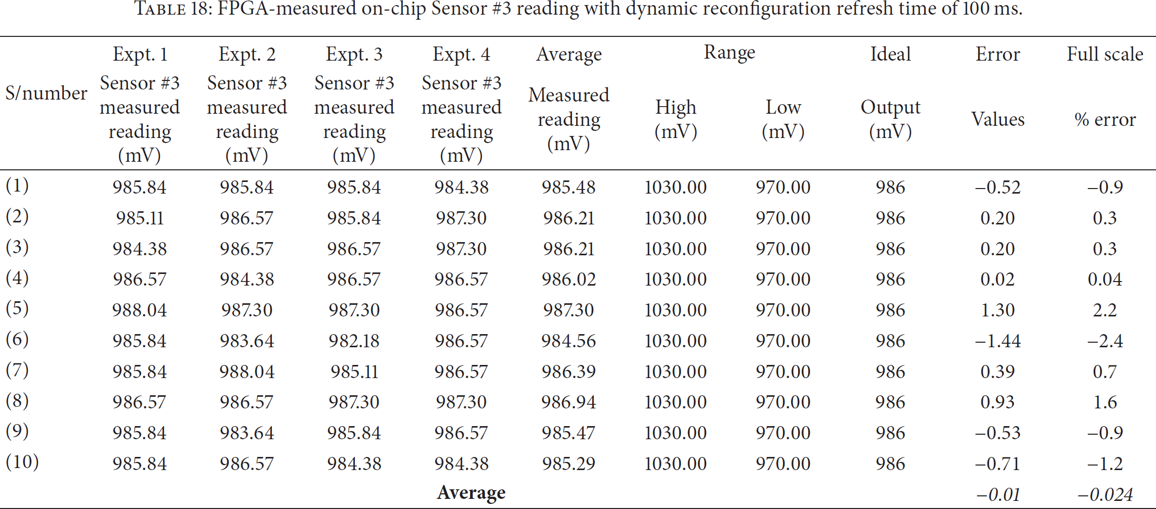
FPGA-measured on-chip Sensor #3 reading with dynamic reconfiguration refresh time of 100 ms.
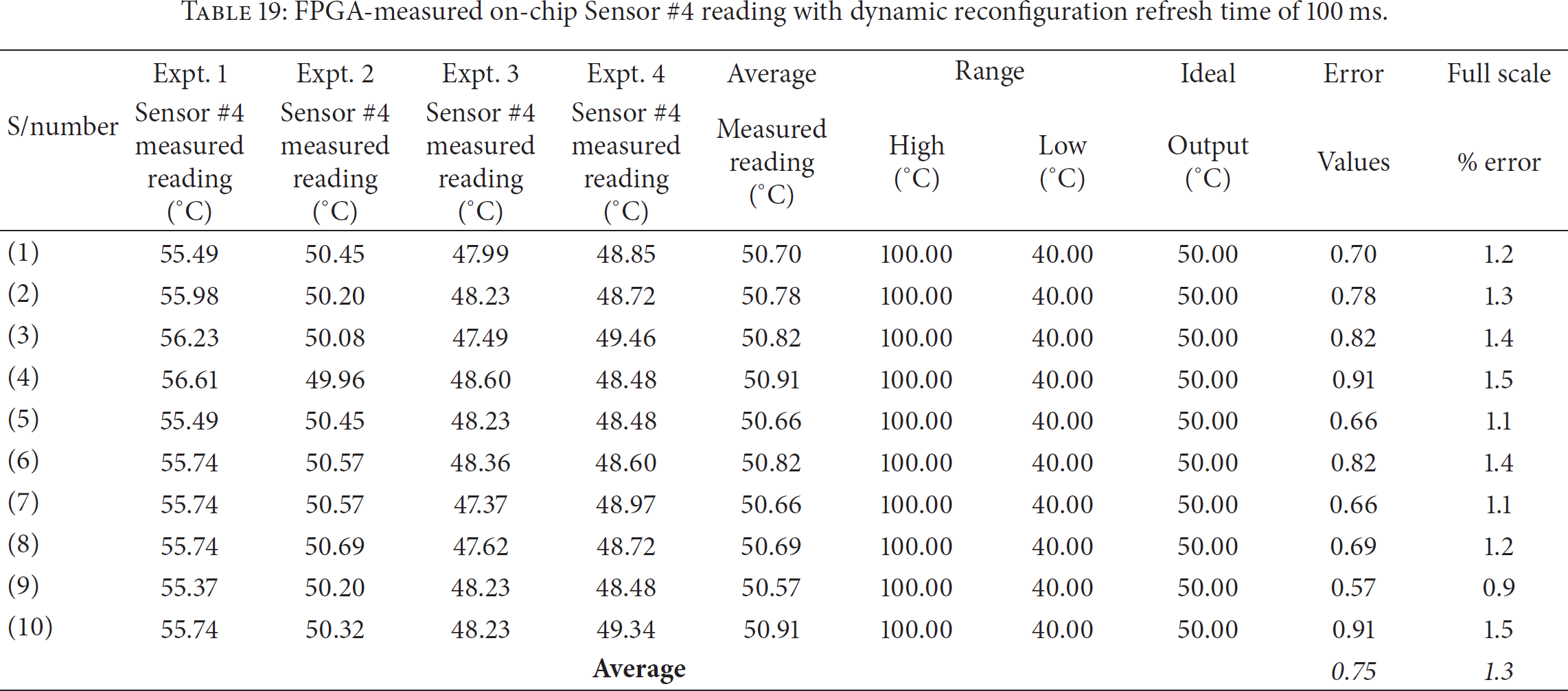
FPGA-measured on-chip Sensor #4 reading with dynamic reconfiguration refresh time of 100 ms.
FPGA-measured on-chip Sensor #5 reading with dynamic reconfiguration refresh time of 100 ms.

Comparison results of the sensor reading accuracy versus dynamic reconfiguration refresh time.

6.1. Effect of Dynamic Reconfiguration Refresh Time on an FPGA-Measured On-Chip Sensor Reading Accuracy
Tables 6–10 list the FPGA-measured on-chip sensor readings with the dynamic reconfiguration refresh time set at 1000 ms. The range of operation and the ideal output of each sensor are specified and listed in the tables. The averaged FS percentage errors of the five sensors are as follows: Sensor #1 = −0.7% FS, Sensor #2 = −0.1% FS, Sensor #3 = 0.8% FS, Sensor #4 = 0.1% FS, and Sensor #5 = 0.4% FS. This result indicates that the accuracy of the measured sensor values is influenced by the reconfiguration refresh time, which shows an accuracy range between −0.7% FS and +0.8% FS.
Tables 11–15 list the FPGA-measured on-chip sensor readings with the dynamic reconfiguration refresh time set at 500 ms. Here, the averaged FS percentage errors for the five sensors are as follows: Sensor #1 = −0.6% FS, Sensor #2 = −0.6% FS, Sensor #3 = +0.2% FS, Sensor #4 = +1.1% FS, and Sensor #5 = 0.3% FS. The averaged FS accuracy lies between −0.6% FS and +1.1% FS, which illustrates a better accuracy compared with reconfiguration refresh time of 100 ms.
Tables 16–20 show the FPGA-measured and controlled on-chip sensors readings with the dynamic reconfiguration refresh time set at 100 ms. The averaged percentage accuracy of Sensor #1 FS is −0.6% FS, Sensor #2 = −0.3% FS, Sensor #3 = −0.024% FS, Sensor #4 = 1.3% FS, and Sensor #5 = 0.4% FS. From Tables 16–20, we can observe that the FS percentage accuracy lies from −0.6% FS to +1.3% FS. This result shows a low accuracy at FS as compared with the dynamic reconfiguration refresh times of 500 and 1000 ms. Table 21 shows the comparison results of the sensor reading accuracy versus the dynamic reconfiguration refresh time. We can observe that the FS percentage error with dynamic refresh time of 100 ms is between −0.6% FS and +1.3% FS, that of 500 ms is between −0.6% FS and +1.1% FS, and that of 1000 ms is between −0.7% FS and +0.8% FS. This result shows that the lower FS percentage error range is almost the same (i.e., −0.6% FS and −0.7% FS) for all sensors irrespective of the dynamic refresh time. However, at higher FS percentage error rate, a significant difference in accuracy exists with different dynamic refresh time, that is, +0.8% FS, +1.1% FS, and +1.3% FS. Therefore, the dynamic reconfiguration refresh time of 1000 ms produces highly accurate FPGA-measured on-chip sensor readings.
In conclusion, the dynamic reconfiguration refresh time affects the accuracy of the FPGA-measured on-chip sensor readings. We determined that the dynamic reconfiguration refresh time of 1000 ms provides highly accurate FPGA-measured and controlled on-chip sensor readings across the five different on-chip sensors.
7. Conclusions
In this research paper, we have proposed the design of efficient and high-speed circuit for real-time monitoring and control of on-chip sensor network for FPGAs. We developed the autonomous sensor agents implemented in the FPGA-based NI to be dynamically configured and to communicate the dynamic ambient parameter changes to the monitoring and control hardware unit. The ultimate goal of this research is to design low-cost, low power, and high accuracy real-time monitoring mechanism using autonomous sensor agents as well as a dynamic reconfiguration control of on-chip sensor network environment using FPGAs. We presented a detailed design procedure and a case study to demonstrate the applicability of the proposed approach. We showed that the proposed approach uses low FPGA logic resources and low power consumption compared with previous approaches, validating its suitability in real-system development. Furthermore, we demonstrated that, by collecting the dynamic and real-time monitoring parameters in terms of temperature and voltage variations, the system can adapt and improve the utilization of FPGA logic resources and power consumption. Experimental results from the FPGA-measured on-chip sensor readings showed high precision and accuracy in the measured voltage and temperature. We found that a dynamic refresh time of 1000 ms produces the best FPGA-measured and controlled on-chip monitored sensor readings as compared with the 100 and 500 ms refresh time. The proposed design techniques, framework, and protocol will assist network engineers and system designers with a flexible and efficient real-time monitoring and control scheme for large and complex FPGA-based on-chip sensor networks and other related remote-sensing applications.
Footnotes
Conflict of Interests
The authors declare that there is no conflict of interests regarding the publication of this paper.
Acknowledgments
This work was supported in part by the Chosun University Research Fund 2015. The authors would also like to thank Xilinx Corporation for providing the Zynq FPGA board and Vivado design tools. Special thanks are owed to the Associate Professors Antonio Filieri of Stuttgart University, Germany, and Martina Maggio of Lund University, Sweden, and Schloss Dagstuhl, Leibniz Centre for Informatics, Germany, for the Dagstuhl GI seminar 14382 “Control Theory Meets Software Engineering” 2014. Finally, they thank the Synopsys Corporation for providing the SaberRD integrated design environment and tools.