
Abstract
The paper proposes an efficient multiplexing scheme that is easy to realize synchronous sampling in a multichannel acquisition system with the large number of analogue inputs and different sampling rates. And then, a simple improved sampling control method is also employed to improve the performance. All the technology of implementing the method is by using a low-cost field programmable gate array (FPGA). A sampling lookup table is built by the rule-based synchronous sampling frame structure for the input analogue multiplexers and stored into the internal block RAM resource in the FPGA to reduce the internal wiring resources and optimize the utilization. The improved sampling method obtains several samples in a sampling period and gets the average value as the final output for the sampling channel. In addition, the standard sine wave FFT test method is implemented to test the dynamic parameters of the acquisition channels. The experiment results show that the dynamic performance of the acquisition system is significantly improved. The proposed multiplexing scheme and sampling method can easily be reconfigured for other applications.
1. Introduction
Nowadays, data acquisition systems are widely used in aerospace system testing, industrial automation, medical diagnosis, communications, and other various industries. They usually employ different structures in terms of different applications and have some vastly variations, which can be seen in the performance and cost [1–3]. In some applications, a large number of parameters need to be measured, and these desired signals always have different frequency bandwidths with the range from Hz to kHz. For example, heartbeat, blood pressure, and the lung sound are needed to be acquired for the health monitoring. And in case of the aircraft's flying test, parameters of the pressure, temperature, shock, and angular velocity are required to be measured. The abundance and diversity of the tested parameters are always higher in these applications. This will pose challenges for the measurement systems. Some multichannel acquisition systems apply a dedicated analogue-to-digital converter (ADC) for each channel to acquire the signals simultaneously. However, those hardware configurations limit the amount of channels that can be acquired and bring more cost and power consumption [4]. If simultaneous sampling for all channels is not necessary, some use a single A/D converter and multiplexers to sample the input signals, thus reducing the system complexity and cost [5, 6]. These systems are frequently used to sample the same type of multiple elements with the same sampling rate. If the input channels have different sampling frequencies, all the input channels would use the highest frequency among the sampling frequencies as a fixed sampling rate. It usually results in unnecessary data that requires more data storage capabilities.
In the paper, a low-cost FPGA-based multichannel system is presented for heterogeneous inputs. A single high speed successive approximation (SAR) A/D converter and several multiplexers are used to sample the multiple heterogeneous signals, and FPGA modules are used to implement sampling channel control and analogue to digital conversion. The paper presents the high efficiency multiplexing scheme for multichannel data acquisition system with different sampling frequencies. An FPGA-based multiplexing scheme lookup table, which can be reconfigured according to the different application requisitions, is established for the channel control reliably, and it can easily be reconfigured for other applications. In addition, to improve the measurement accuracy as much as possible is the primary goal in a data acquisition system. In a number of high-precision requirements, such as weak signal detection technology, high-resolution ADC chips are usually used to achieve high-precision measurements. In addition to using the high-resolution ADC chips, some other technologies are used to obtain higher resolution. Oversampling and averaging methods are mentioned to improve the measurement resolution [7–10]. In this paper, a simple way which makes the reference to the oversampling and averaging theory is proposed to improve the acquisition accuracy of the multichannel acquisition system.
2. Related Works
Multiplexing is typically done with SAR A/D converters. It has the characteristic of medium resolution and speed, small chip area, and low power consumption, and so forth. Moreover, it is convenient to make multichannel conversions because their sample times can be made arbitrarily. Due to their mixed advantages in resolution, speed, power, and cost, SAR ADCs are widely applied in industry controlling, medical instruments, auxiliary analogue-to-digital interfaces of microprocessors, and so on [11, 12]. In recent years, FPGA with the advantages of design flexibility and adaptability is the current trend for the digital implement [13–15]. As shown in Figure 1, the multichannel acquisition system is composed of a single high speed SAR A/D converter, a FPGA module, a flash storage module, a USB controller module, several analogue multiplexers, and signal conditioners. The brief workflow of the multichannel acquisition system is as follows. First, the input analogue signals are modulated by the conditioner to meet the back-end ADC's requirement. The signal conditioner is used for gain controlling, offset adjustment, noise reduction, and impedance transform. The circuit of the conditioner usually consists of the operational amplifier, several resistances, and capacitances. And they can adjust the amplitude of the inputs to the maximum range of the ADC. Then, the FPGA module is designed to complete the implementation of sampling channel control, analogue-to-digital conversion, and transports data between a multiplexed data stream and channel data buffers using a user defined format. Flash module is used to store the quantization. Finally, a computer is used to reveal the data from the flash storage module by the USB controller and analyze the data. This paper puts emphasis on introducing the technologies for the multiplexing and the improved sampling control method.

General schematic for multichannel acquisition system.
3. Multiplexing Scheme
3.1. Sampling Frame Format
The proposed multichannel data acquisition system uses a single SAR ADC to adopt a fixed sampling rate and in turn encodes it by the sequence. If the input signals have the same frequency, it is appropriate for systems with equal channel sampling frequencies. However, when the number of the measured signals is large and has various rates, frequently in several orders of magnitude, it does not provide desirable results. In this paper, a concept of a sampling data frame format which consists of several subframes is proposed to achieve uniform sampling for each channel. The channel is assigned a different number of the slots of the frame format. The ADC completes the conversion at evenly spaced points in time domain in accordance with sequence of the sampling frame format. Table 1 shows the structure of the sampling frame. The sampling data frame consists of frame flag, time stamp, and channel_data_N fields. The frame flag is the specific data structure which occurs at both the beginning and end of each frame to delimit the frames for data merging or postprocessing. It usually takes two unique bytes to represent the flag, such as
Multichannel sampling frame format.
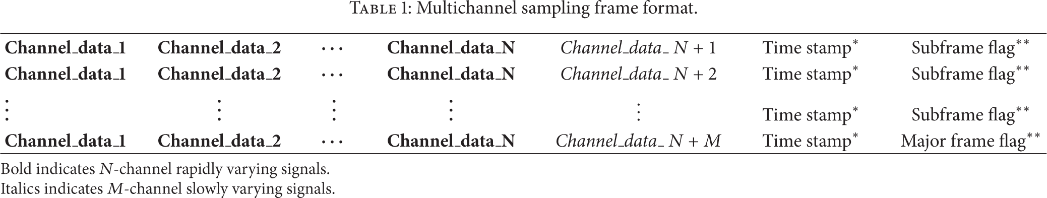
Bold indicates N-channel rapidly varying signals.
Italics indicates M-channel slowly varying signals.
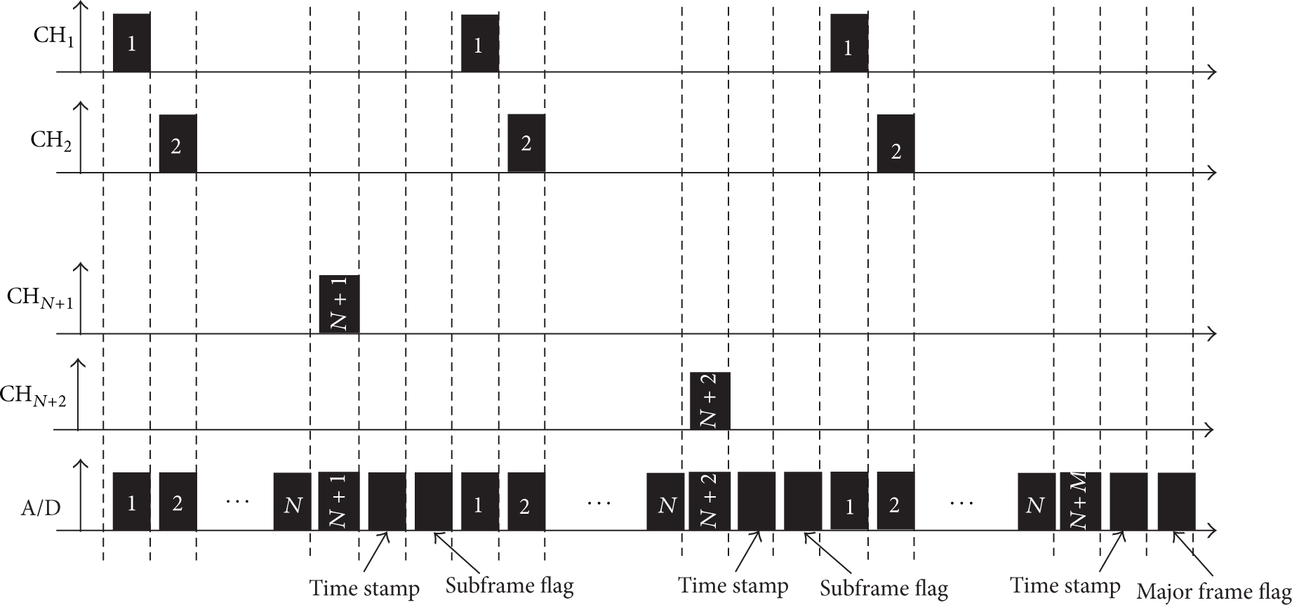
Channel sampling sequence with the proposed sampling frame.
3.2. FPGA-Based Multiplexing Scheme Lookup Table
Take a 64-channel acquisition module for example. Four single 16-to-1 multiplexers (ADG706) are used to realize the switching between 64 inputs. A 16-bit SAR ADC (AD7667), with up to 1 Msps rate, is used to complete the digitization of the input analogue signals. A Xilinx's FPGA (Spartan-3 XC3S400) is designed to control the sampling for ADC, switching, and processing, if it is needed. The ADG706 is controlled by the 4-bit address lines and an EN input. The 4-bit address lines A0, A1, A2, and A3 determine one of the 16 inputs to the common output. The EN input is used to enable or disable the device. In order to control the switching of 64-channel properly, the corresponding address lines of the multiplexers are connected together, separately. But the EN control lines use four separate control lines. So we can encode the eight control lines and build the lookup table according to the sampling frame format. The control logic programming in FPGA enables switching channels based on the sequence of the lookup table. Four EN inputs on the devices and the common 4-bit binary address lines A0, A1, A2, and A3 are organized into an 8-bit binary data.
The Xilinx Spartan-3 FPGA offers a flexible programmable architecture and a rich selection of built-in blocks. These include abundant block or distributed RAM resources and clock management blocks. In the paper, an efficient method is proposed to use block RAM resource in FPGA to establish a sampling channels lookup table to store the coding for multiplexing scheme. The control logic takes data from the lookup table and turns it into the channel switching signals. Compared to programing the channel switching logic directly, the proposed method is clearly more flexible and easier to implement. The FPGA-based multiplexing scheme lookup table is built in the following procedure.
First, a txt-file being named “frame.txt” is created by using a text editor. As shown in Figure 3, the data which are written in the txt-file are coded according to the sampling frame format for the acquisition channels.
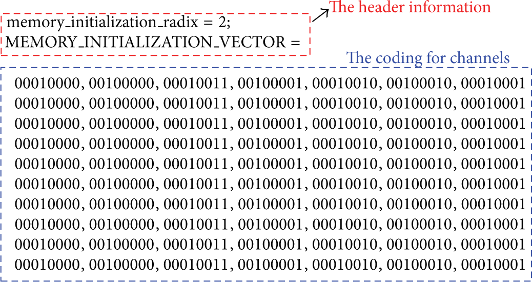
Multiplexing scheme lookup table.
Next, the suffix of the object file is changed to “.coe” from “.txt”. Open the file and add a semicolon to the last line of the file. Then, the header information is required to add at the beginning of the file (Figure 3). At last, save this file and close the editor.
Finally, using Xilinx ISE Design Suite, we apply IP core technology to realizing ROM module by configuring block RAM resource in FPGA and load the “frame.coe” file into the ROM [16].
The sampling lookup table built by the interior block RAMs resource is shown in Figure 4. The addresses of the memory space all correspond to the time slots in the sampling frame. When triggering the acquisition, the address is increased in succession sequence from zero address. The marking code can be read out to implement the channel switching by the control logic. It is demonstrated that this method is suitable for multichannel data acquisition applications by changing the codes in lookup table.

The sampling channel lookup table in FPGA.
The hardware resources illustrated in Figure 5 show the amount of the consumed resources of the proposed lookup table method. Compared with the register and related logic control design method, the FPGA-based multiplexing scheme lookup table method greatly reduces the internal resources and improves software quality and stability. The horizontal axis shows the internal resources: flip flops, 4-input LUTs, slices, and block RAM in Xilinx FPGA, and the vertical axis represents the amount of the consumed resources.

FPGA resource consumption with different control methods.
4. Improved Sampling Method
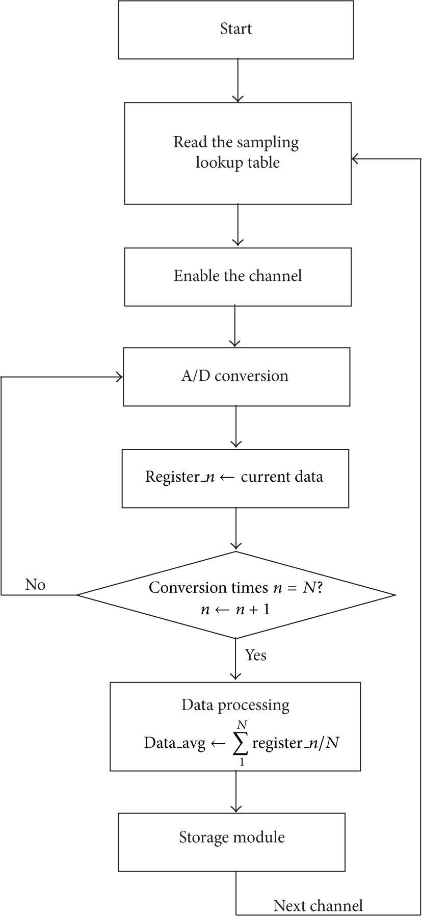
The oversampling method is a widely used technique for improving the ADC's revolution. The white noise accompanies the signal and the increase of each bit of the resolution can be achieved via fourfold sampling frequency theoretically. Because the SAR ADC's sample times can be made arbitrarily within device limits, the paper presents a simple improved sampling method by using oversampling and averaging technology to improve the performance of the system. Figure 6 shows the flowcharts of the improved sampling cycle. As shown in the figure, after reading the data out of the lookup table, the FPGA does the channel switching. Then, wait for the signal stability and complete a conversion. The improved sampling method carries out multiple conversion operation to obtain samples after gating the sampling channel. The averaging operation is conducted for the samples in the FPGA, and the mean is translated as the final output for the sampling channel.
Improved sampling procedure.
Compared with the averaging method using the computer, the FPGA-based oversampling and averaging algorithm will not bring the extra storage space and can meet the real-time demand. Generally speaking, it is difficult to perform the division operation by using a cost-effective FPGA. But some special methods are designed to achieve a similar division function. It is known that a right shift by N of the binary data is equivalent to dividing by
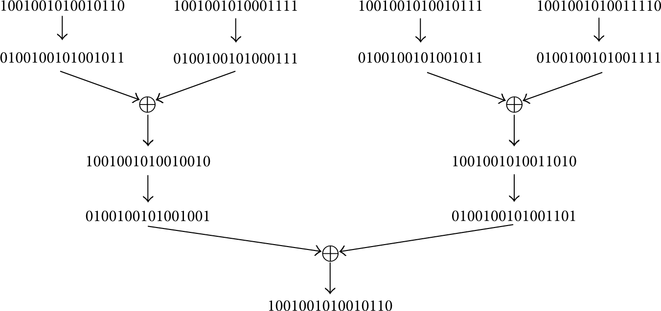
The averaging operation in FPGA.
First, four pieces of binary data are implemented once right shift and insert value 0 bits into the most significant bit to produce four pieces of new data.
Second, each of the two pieces of data completes the summation operation.
Third, two pieces of generated data are implemented once right shift and insert value 0 bits into the most significant bit.
Finally, the sum is the mean of the proposed four 16-bit binary data finally.
The improved sampling method is to optimize the internal resources of the FPGA and does not need any additional hardware. The amount of the consumed resources in different samplings by N

FPGA resource consumption with different sampling methods.
5. Limitations
As discussed in Sections 2 and 3, the use of the sampling frame format method for multichannel acquisition applications is constrained by the conversion rate of ADC 
The major factor affecting such limitation is the settling time. As shown in Figure 9, the settling time in the multiplexed systems is far more than the converter latency in a sampling cycle. If the start time conversion and switching interval are too short, the signal will be sampled in an instability state, which will induce serious distortion. Suppose that the total sampling rate of a multichannel acquisition system is 

Settling time for channel switching.
The settling time 
If the proposed improved sampling method in Section 4 is used to acquire the digitalization, the limitation also exists. The method needs to complete multiple conversion operation to obtain samples in 
6. Performance Evaluation
6.1. Experimental Setup
For validating our method, the test platform setup for acquisition system dynamic testing is illustrated in Figure 10. A sine wave is generated by an arbitrary wave generator (AWG) and connected to one of the channels. The multichannel acquisition system is introduced in Section 2. A single 16-bit SAR ADC (AD7667) and several high-speed analogue multiplexers (ADG706) are used to sample the analogue inputs; FPGA (XC3S400) modules are used to implement sampling channel control and analogue to digital conversion. The standard sine wave FFT test method is used to obtain the dynamic performance of the acquisition channel. The method validation for dynamic performance is performed by evaluating the total harmonic distortion (THD), signal to noise and distortion (SINAD), signal-to-noise rate (SNR), and effective number of bits (ENOB) of the multichannel acquisition system [17, 18]. The data analysis has been implemented using the Matlab R2013b software in a computer. As discussed in Section 4, four sampling methods are applied to the acquisition system, respectively.

Experimental setup to test the performance.
6.2. FFT Test and Dynamic Characteristics of the Acquisition Channel
In the test, the AWG is adopted to generate a 500 Hz sine wave signal with 2.5 Vpp amplitude. The channel sampling rate is 9.76 kHz. 81920 samples are acquired and processed in the frequency domain. Moreover, the Hanning window is used for all the processes. Figure 11 shows a comparison with power spectrum of the sine wave FFT test between the different sampling methods. It is clear that the harmonics are very strong. The test results of the dynamic parameters and test conditions are listed in Table 2.
Dynamic test results (


The power spectrum of the sine-wave input (
Sinusoidal signals, varying from 10 Hz to 850 Hz, are generated with sequential increment by 40 Hz to complete the FFT test, and the amplitude of the sinusoidal signal is not changed. Due to the frequency differences among the input signals, there are slight differences in the measured results. Figure 12 shows the dynamic characteristics and the improvements in different sampling methods, respectively. The improved method had better results for the dynamic characteristics. The ENOB improvements ranged between 0.4 bits and 0.5 bits when using 6-time sampling. The magnitudes of these improvements in average were 0.4 bits and 0.28 bits for 4-time sampling and 2-time sampling. The average SNR improvement over the whole range for normal sampling is 3.01 dB when using 2-time sampling, 5.39 dB when using 4-time sampling, and 5.92 dB when using 6-time sampling. The average SINAD improvement is 1.67 dB, 2.39 dB, and 2.79 dB when using 2-time, 4-time, and 6-time sampling methods, respectively. The THD improvements also ranged between 0.1 dB and 0.5 dB in the proposed sampling methods. The comparison analysis has demonstrated that the proposed method can improve the dynamic performance effectively.

Dynamic characteristics and improvements of the acquisition channel. The blue, red, green, and black curves represent the normal sampling, 2-time sampling, 4-time sampling, and 6-time sampling, respectively.
7. Conclusion
We have developed an FPGA-based multichannel acquisition system along with a high speed SAR ADC and several multiplexers for heterogeneous inputs. The single SAR ADC can be efficiently used with the optimal multiplexing scheme to acquire multiple inputs. A high efficiency multiplexing scheme has been successfully developed for increasing flexibility and enabled the module reuse in different applications. This design can reduce the size, the cost, and the power consumption of the circuit. The reconfigurability based on the FPGA is the best solution to be reused with different configurations. A simple improved sampling method using oversampling and averaging technology to optimize the performance of the system has been implemented in the FPGA. The method obtains several samples in a sampling period and gets the average value as the final output for the sampling channel. The improving method implemented on FPGA requiring low hardware resources can enhance the resolution of the acquisition system, and it is applicable for different data acquisition applications.
Footnotes
Conflict of Interests
The authors declare that there is no conflict of interests regarding the publication of this paper.
Acknowledgment
This project is supported by the National Nature Science Foundation of China (50905169).