
Abstract
This paper proposes a novel hardware architecture for real-time face detection, which is efficient and suitable for embedded systems. The proposed architecture is based on AdaBoost learning algorithm with Haar-like features and it aims to apply face detection to a low-cost FPGA that can be applied to a legacy analog video camera as a target platform. We propose an efficient method to calculate the integral image using the cumulative line sum. We also suggest an alternative method to avoid division, which requires many operations to calculate the standard deviation. A detailed structure of system elements for image scale, integral image generator, and pipelined classifier that purposed to optimize the efficiency between the processing speed and the hardware resources is presented. The performance of the proposed architecture is described in comparison with the detection results of OpenCV using the same input images. For verification of the actual face detection on analog cameras, we designed an emulation platform using a low-cost Spartan-3 FPGA and then experimented the proposed architecture. The experimental results show that the processing time for face detection on analog video camera is 42 frames per second, which is about 3 times faster than previous works for low-cost face detection.
1. Introduction
Face detection is the process of finding the locations and sizes of all possible faces in a given image or in video streams. It is the essential step for developing many advanced computer vision and multimedia applications such as object detection and tracking [1–3], object recognition [4–6], privacy masking [7], and video surveillance [8, 9]. The object detection scheme proposed by Viola and Jones [10] is one of the most efficient and widely used techniques for the face detection from the advantage of its high detection rate and fast processing.
The recent trend in video surveillance is changed to IP network cameras. But the analog video cameras are still widely used in many surveillance services because of availability, cost, and effectiveness. The face detection now available with IP cameras is not available in analog video cameras. We would like to propose an alternative method, which can provide face detection in analog video cameras.
Recently, real-time processing of the face detection is required for embedded systems such as security systems [11], surveillance cameras [12], and portable devices. The challenges of the face detection in embedded environments include an efficient pipelined design, the bandwidth constraints set by low cost memory, and an efficient utilization of the available hardware resources. In addition, consumer applications require the reliability to guarantee the processing deadlines. Among these limitations, the main design concerns for face detection on embedded system are circuit area and computing speed for real-time processing. The face detection, however, essentially requires considerable computation load because many Haar-like feature classifiers check all pixels in the images. Therefore, the design methods to achieve the best trade-off between several conflicting design issues are required.
Currently, Viola-Jones face detection scheme is used in personal computer system in the form of the Open Computer Vision Library (OpenCV) [13]. However, the implementation of the OpenCV's face detection on the embedded system is not a suitable solution because the computing power of the processor used in an embedded system is not as powerful as those in PCs. This disparity between the real-time processing and the limited computing power clearly shows the necessity of coprocessor acceleration for image processing on the embedded system.
In general, the hardware system is implemented on an application specific integrated circuit (ASIC) or on field-programmable gate arrays (FPGAs). Although slower than ASIC devices, the FPGA has the advantage of the fast implementation of a prototype and the ease of design changes. Recently, the improvement of the performance and the increase of the density of FPGAs such as embedded memory and DSP cores have led to this device becoming a viable and highly attractive solution to computer vision [14–16].
The high-speed vision system developed so far accelerates the computing speed by using massively parallel processors [17, 18] or by implementing the dedicated circuits in reconfigurable hardware platform [19–25]. However, the previous researches focused on the enhancement of the execution speed instead of the implementation on the feasible area, which is the real concern of embedded systems. Only few attempts have been made to realize the Viola-Jones face detection scheme in embedded systems [26–29]. Although these approaches have been tried to develop an effective detection system for embedded system, their performance seems to be still insufficient to meet the real-time detection. Therefore, a spatially optimized architecture and a design method that enhances the detection speed and can be implemented on a small area are required.
In this paper, we present efficient and low-cost FPGA-based system architecture for the real-time Viola-Jones face detection applicable to legacy analog video cameras. The proposed design made an effort to minimize the complexity of architecture for implementing both integral image generator and classifier. The main contributions of this work are summarized as follows. Firstly, we propose an efficient method to calculate the integral image using the cumulative line sum. Secondly, we suggest an alternative method to avoid division, which requires many operations to calculate the standard deviation. The integral image window is generated by the combination of the piped register array, which allows fast computation of integral image as introduced in [22], and the proposed compact integral image generator. The classifier then detects a face candidate using the generated integral image window. Finally, the proposed architecture uses only one classifier module, which consists of 7-stage pipeline based on training data of OpenCV with 25 stages and 2,913 features. As the result of applying the proposed architecture, we can design a physically feasible hardware system to accelerate the processing speed of the operations required for real-time face detection in analog video cameras.
2. Related Works
In this section, we firstly give a brief introduction of face detection based on AdaBoost learning algorithm using Haar-like features. Then we evaluate the most relevant previous works in the literature.
2.1. AdaBoost Face Detection
Viola and Jones proposed a robust and real-time object detection method using AdaBoost algorithm to select the Haar-like features and to train the classifier. They selected a small number of weak classifiers and then these classifiers combined in a cascade to construct strong classifiers. Haar-like feature consists of several black and white rectangles and each feature has predefined number and size of rectangles. Figure 1(a) shows some examples of Haar-like feature and Figure 1(b) shows how Haar-like features are applied to a subwindow for face detection.

Haar-like features: (a) examples of Haar-like features, (b) Haar-like features applied to a subwindow, (c) integral image of pixel
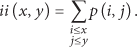
The computation of a Haar-like feature involves the subtraction of the sum of the pixel values in the black rectangle from the sum of pixel values in the white rectangle of the feature. To speed up the feature computation, Viola and Jones introduced the integral image. The integral image is a simple transformation of the original input image to the alternative image where each pixel location represents the sum of all the pixels to the left and above of the pixel location as shown in Figure 1(c). This operation is described as follows, where
The computation of the integral image for rectangle D in Figure 1(d) can be calculated by two additions and two subtractions using the integral image values of four corner points:
To achieve fast detection, Viola and Jones also proposed a cascade structure of classifier. Each stage of the cascade consists of a group of Haar-like features selected by AdaBoost learning algorithm. For the first several stages, the classifiers are trained to reject most of the negative subwindows while detecting almost all face-like candidates. This architecture can speed up the detection process dramatically because most of negative images can be discarded during the first two or three stages. Therefore, the computation effort can be focused on face-like subwindows. Subwindows are sequentially evaluated by stage classifiers and the result of each Haar-like feature in a stage is accumulated. When all the features in a stage are computed, the accumulated value is compared with a stage threshold value to determine if the current subwindow is a face-like candidate. The subsequent stage is activated only if the previous stage turns out to be a positive result. If a candidate passes all stages in the cascade, it is determined that the current subwindow contains a face.
2.2. Related Works
Since Viola and Jones have introduced a novel face detection scheme, numerous considerable research efforts have already expended on the efficient implementation of their scheme. Most of these literatures mainly focused on the optimization of feature calculation and cascade structure of classifiers because they are the most time consuming part in the detection system.
Lienhart and Maydt [30] were the first to introduce the face detection algorithm into Intel Integrated Performance Primitives, which was later included in OpenCV library [13]. The optimized code for x86 architecture can be detected accurately on an image of 176 × 144 with 2 GHz Pentium-4 processor in real-time. However, on embedded platforms, this performance is much poorer than on the desktop platform. A 200 MHz ARM9 processor can only detect the same resolution image at the speed of 7 fps, which is far from real-time execution. This means that the face detection is still a time consuming process on embedded platforms. In order to detect a face in an image, a massive number of subwindows within each image must be evaluated. Therefore, a hardware design of AdaBoost algorithm could be an alternative solution for embedded systems. Theocharides et al. [18] proposed a parallel architecture using a structure called CDTU (Collection and Data Transfer Unit) array on an ASIC platform to accelerate the processing speed. The simulation results in their paper reported that they obtained a rough estimate of 52 frames per second targeting 500 MHz clock cycle. However, the CDTU architecture consumes massive hardware resources, which is difficult to adopt in embedded systems. Moreover, VLSI technology requires a large amount of development time and cost and it is difficult to change design. Recently, much attention has been paid to implement a face detection system using FPGA platform. FPGA can provide a low-cost platform to realize the face detection algorithm in a short design time with the flexibility of fine tuning the design for more parallel operations as needed. In recent years, new generations of FPGAs with embedded DSP resources have provided an attractive solution for image and video processing applications. In the work presented by Shi et al. [19] some optimization methods are suggested to speed up the detection procedure considering systolic AdaBoost implementations. The proposed work introduces two pipelines in the integral image array to increase the detection process: a vertical pipeline that computes the integral image and a horizontal pipeline that can compute a rectangle feature in one cycle. However, their results are not hardware implementation but come from the cycle accurate simulation. Cho et al. [20] proposed a parallelized architecture of multiple classifiers for a face detection system using pipelined and parallel processing. They adopted cell array architecture for the main classification modules. The integral image is generated for each subwindow and is then used for classification through a cell array. Recently, Hiromoto et al. [21] proposed a hybrid model of face detection architecture consisting of parallel and sequential modules. To achieve high speed detection, the parallel modules are assigned to the early stages of the algorithm which are frequently used whereas the latter stages are mapped onto sequential modules as they are rarely executed. However, the separation of the parallel and sequential stages requires additional hardware resources to hold the integral image values for current subwindow to process in sequential stages while parallel stages compute a new subwindow. Moreover, the detailed experimental results and analysis of the implemented system are not discussed.
Lai et al. [22] presented a hardware architecture that employs very similar architecture to the ones presented in [20, 21]. They used a piped register module for integral image calculation with 640 columns and 22 rows. According to their report, it can achieve theoretical 143 fps detection for 640 × 480-pixel images. However, they used only 52 classifiers in a single stage. Because of their small number of cascade stages and classifiers, their results show lower detection rate and higher false alarm rate than OpenCV's implementations. Gao and Lu [23] presented an approach to use an FPGA to accelerate Haar-like feature based face detection. They retrained the Haar-like classifier with 16 classifiers per stage. However, only classifiers are implemented in the FPGA. The integral image computing is processed in a host microprocessor.
The aforementioned approaches achieve fast detection but they still require too much hardware resources to be realized in embedded systems. Bigdeli et al. [26] studied the effects of replacing certain software bottleneck operations by custom instructions on embedded processors, Altera Nios II processor, especially the image resizing and floating point operations, but did not fully implement the entire algorithm in hardware. A simple version of the algorithm was proposed in [27] where techniques such as scaling input images and fixed-point expression to achieve fast processing with a smaller circuit area were used. The architecture presented in [27] was reported to achieve 15 fps at 91 MHz. However, the image size is too small (120 × 120 pixels) to be practical and only three stages of classifiers are actually implemented. Another low-cost architecture implemented on an inexpensive ALTERA Cyclone II FPGA was reported by Yang et al. [28]. They used a complex control scheme to meet hard real-time deadlines by sacrificing detection rate. The frame rate of this system is 13 fps with low detection rate of about 75%. On the other hand, Nair et al. [29] proposed an embedded system for human detection on a FPGA platform, which performed on an input image of about 300 pixels. However, the reported frame rate was only 2.5 fps. Although they insist that their implementations target embedded system, the disadvantage of such designs is low pixel images or a low performance, which is far from real-time detection in embedded systems.
3. Proposed Hardware Architecture
The structure of the proposed face detection system for analog video camera is shown in Figure 3. In the proposed design, we made an effort to minimize the complexity of the architecture for implementing each block. We also considered the contribution for the trade-off between the performance and the consuming hardware resources. The proposed method is able to detect a face in conventional analog video cameras without a large-scale change of the system. Our method only reads the analog input video signal through the physical wiring and detects faces in each input frame. The detection result is then transmitted to a camera or system by using the general-purpose serial interface. Therefore, there is almost no effect on the operation of conventional systems.
The proposed architecture consists of three major blocks: an image scale block (ISB), an integral image processing block (IPB), and a feature processing block (FPB). For the video image acquisition, we used a commercial device, which supports the analog-to-digital conversion and the decoding of a composite signal into a NTSC signal. The A/D converter in the image acquisition module converts the analog image signals into digital image data. The video sync module converts digital image data to BT.656 video protocol.
The basic flow of the proposed architecture is as follows. The ISB receives the input video frame and scales down the frame image. After a frame image is stored, the operating state is changed to calculate the integral images for each subwindow of the current frame. The IPB is responsible for generating and updating the integral image for the integral image array. The operation state is then moved to the face detection state, which is processed in the FPB. The classifier in the FPB evaluates the integral image transferred from IPB and provides the output of the detection results.
3.1. Image Scale Block (ISB)
The ISB receives the input video image frames from the image acquisition module and scales down each frame image. The image scaling is repeated until the downscaled image is similar to the size of the subwindows. The video interface module of the ISB receives image frame in the row-wise direction and saves image pixels into the frame image buffer.
The detailed structure of the video interface module is shown in Figure 4. The data path receives BT.656 video sequences and selects active pixel data regions in the input video packet. The sync control generates the control signal to synchronize the video frame using the embedded sync signals of the BT.656 video sequences such as EAV (end of active video) and SAV (start of active video) preamble codes. The generated control signals are used to generate the address and control signals for managing the frame image buffer.
The frame image buffer stores a frame image at the start of operation. In general, the management of data transmission becomes an issue in embedded video system. The clock frequency of inner modules of the face detection system is running at higher speed than the clock rate of input video sequence. Using a dual-port memory has proven to be an effective interface strategy for bridging different clock domain logics. The frame image buffer consists of a dual-port RAM. Physically, this memory has two completely independent write and read ports. Therefore, input video streams are stored using one port and inner modules read out the saved image using the other one.
The image scale module scales down the frame image stored in the frame image buffer by the scale factor of 1.25. To make downscaled images, we used the nearest neighbor interpolation algorithm, which is the simplest interpolation algorithm and requires a lower computing cost. This module keeps scaling down until the height of scaled frame image is similar with the size of the subwindow size (24 × 24 pixels). Therefore, the image scale module has 11 scale factors (1.250 ~1.2510) for 320 × 240-pixel image. This module consists of two memory blocks (mem1 and mem2). Once the frame image data is saved in frame image buffer, the image scale module starts to generate the first scaled image, which is saved in the mem2. At the same time, the original frame image is transferred to the IPB to start the computing of the integral image. After all the computing of IPB and FPB over the original image is finished, data stored in the mem2 are transferred to IPB and the second scaled image is written back to the mem1. This process is continued until the scaled image is similar to subwindow size. The scale controller generates control signals for moving and storing pixel values to generate scaled images. It also checks the state of video interface and manages the memory modules.
3.2. Integral Image Processing Block (IPB)
The IPB is in charge of calculating integral images, which are used for classification process. Integral image is an image representation method where each pixel location holds the sum of all the pixels to the left and above of the original image. We calculate the integral image by subwindow separately and the subwindow is scanned from the top to the bottom and then from the left to the right in the frame image and the scaled images. In the context of this work, the subwindow is defined as the image region examined for the target objects. The proposed architecture used 24 × 24 pixels as a subwindow.
The integral image generator of IPB performs the precalculation to generate the integral image window. It computes the cumulative line sum (CLS) for the single row (x) of the current processing subwindow as shown in (2), where

The detailed structure of the integral image generator is shown in Figure 5. The line register reads one row of a subwindow from top to bottom lines. Therefore, to store the 24 pixels of image data, the width of the line register requires 24 × 8 bits. Each pixel value for a horizontal line is accumulated to generate the line integral image.
The computing of the line integral image requires the sum of 24-pixel data results in an increase of delay time. To solve this problem, we used a tree adder based on carry-save adders. The tree adder receives eight pixel values and a carry-in as the input variables and outputs eight integral image values corresponding to the input pixels. Therefore, three clock cycles are required to compute a line integral image. This process is performed in parallel and at the same time with the operation of the pipelined classifier module. Thus, when considering overall behavior of the system, it has the effect of taking one clock cycle to compute the integral image. The output of tree adder is fed into corresponding position of the integral image line buffer. Each pixel in the line integral image buffer has a resolution of 18 bits to represent the bit width of integral image pixels for 24 × 24 size of a subwindow. When all the pixel values in the line integral image buffer are updated, the data will be transferred to the bottom line of the integral image window.
The integral image window calculates the integral image of the current subwindow. The structure for integral image window is shown in Figure 6(a). The size of the integral image window is identical to the size of subwindow except the difference of the data width for the pixel values.
The integral image window consists of 24 × 24 window elements (WE) to represent the integral image for the current subwindow. As shown in Figure 6(b), each WE includes a data selector, a subtractor to compute the updated integral image, and a register to hold the integral image value for each pixel. The register takes the pixel value of the lower line (

Cascade structure for Haar classifiers.

Structural overview of the proposed face detection system.

The block diagram of the video interface module.

The block diagram of the integral image generator.
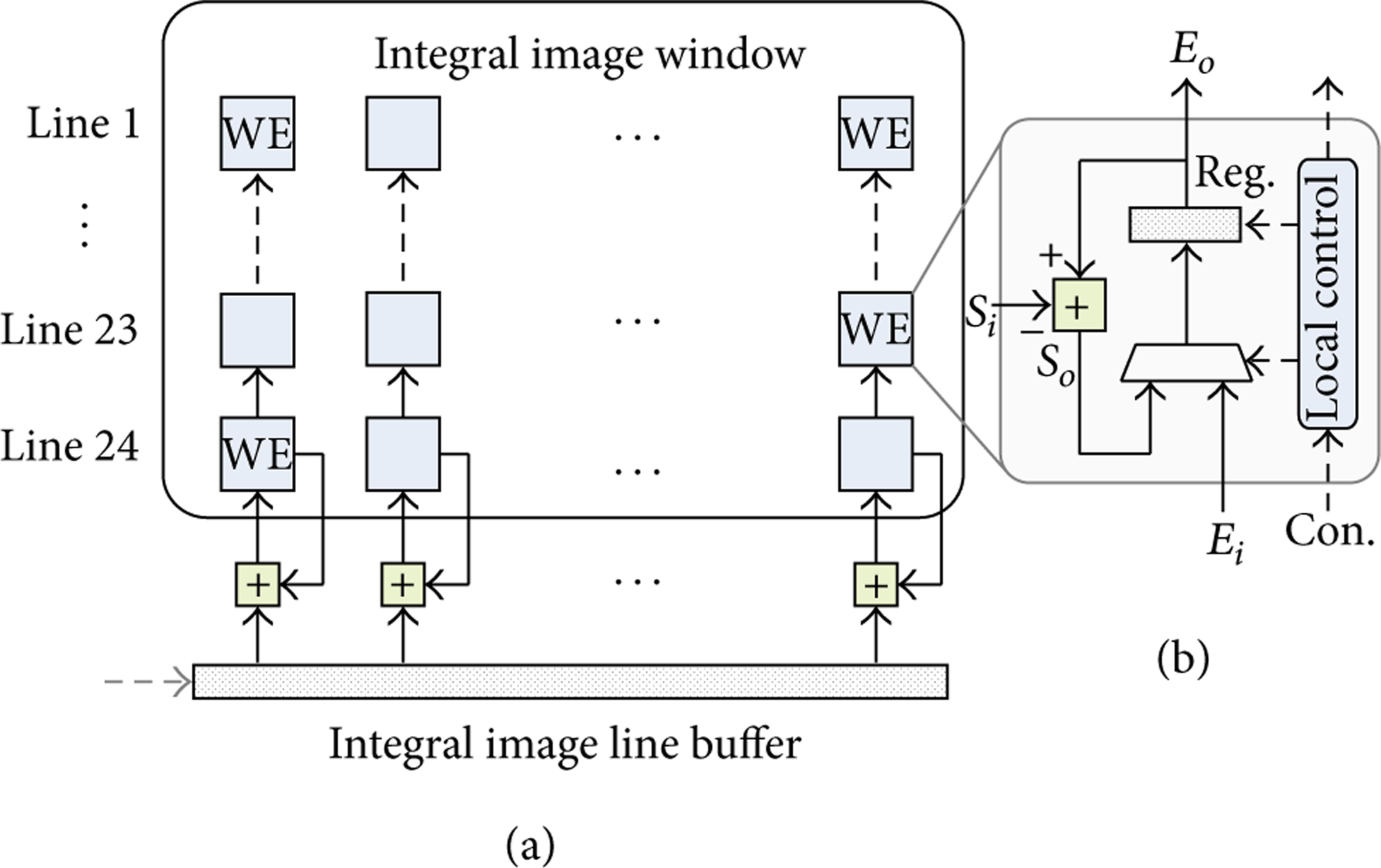
Structure of the integral image window (a) and internal implementations of window element (b).
The data loading for the integral image window can be divided into initial loading and normal loading according to the y coordinate of the left-up corner of the current processing subwindow in the frame image. The initial loading is executed when the y coordinate of the first line in a subwindow is zero (

The WEs at the bottom line of the integral image array accumulate these line integral images and output the accumulated value to the next upper line. The other lines of the integral image array shift current values by one pixel upward. After 24 clock cycles, each WE holds their appropriate integral image values.
The normal loading is executed during the rest of the vertical scan (

During the normal loading, the first 23 lines for the updating integral image array are overlapped with the value of the line 2 to 24 in the current integral image. Therefore, these values are calculated by subtracting the values of the first line (line 1) from the line 2 to 24 in the current integral image and then shift the array one line up. The last line of the updating integral image is calculated by adding the CLS of the new row with the last line of the current integral image array and then subtracting the first line of the current integral image array.
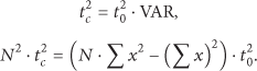
AdaBoost framework uses a variance normalization to compensate for the effect of different lighting conditions. Therefore, the normalization should be considered in the design of the IPB as well. This process requires the computation of the standard deviation (σ) for corresponding subwindows. The standard deviation (σ) and the compensated threshold (

The AdaBoost framework multiplies the standard deviation (σ) to the original feature threshold (
Therefore we can efficiently compute the lighting correction by just using the multiplication and subtraction, since the subwindow size is already fixed and the squared value of the original threshold values can be precomputed and stored in the training set.
The functional block diagram to map the method of (6) in hardware is shown in Figure 7, which is responsible for handling the right part of the second line of (6). The squared image generator module, the left part of Figure 7, calculates the squared integral image values for the current subwindow. The architecture of the squared image generator is identical to that of the integral image generator, except for using squared pixel values and storing the last column's values. Therefore, the computing of the squared integral image requires 24 pixel values in the last vertical line of a subwindow. The output of the squared image generator is the summation of the integral image for squared pixel values (

Structure for squared image generator and variance module.
The other parts of (6) are computed in the variance module, located in the right part of Figure 7. The upper input of the variance module means the integral image value of the coordinate for (24, 24) of the integral image window. The output of the variance module is transferred to the FPB to check with the feature sum of all weighted feature rectangles.
3.3. Feature Processing Block (FPB)
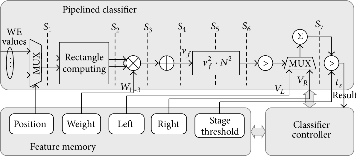
The FPB computes the cascaded classifier and outputs the detected faces' coordinates and scale factors. As shown in Figure 8, the FPB consists of three major blocks: pipelined classifier, feature memory, and classifier controller.
Block diagram for FPB.
The pipelined classifier is implemented based on a seven-stage pipeline scheme as shown in Figure 8. In each clock cycle, the integral image values are fed from the integral image window and the trained parameters of Haar classifier are inputted from the external feature memory. The classifier controller generates appropriate control signals for the memory access and the data selection in each pipeline stage.
To compute rectangle value for each feature of the cascaded classifier, FPB interfaces to the external memory that holds the training data for the features' coordinates and the weights associated with each rectangle. We use one off-chip, 64-bit-wide flash memory for the trained data for coordinates, and weight of features. For storing other trained data, we used the Block RAMs in the target device.
The first phase of the operation for the classifiers is the loading of the features data from the integral image window. In each clock cycle, eight or twelve pixel values of integral image for a feature are selected from the integral image array. To select pixel values, the coordinate data corresponding to each feature is required. We used a multiplexer to select 8 or 12 pieces of data from the integral image array according to the feature data stored in the external memory.
The rectangle computation takes place in the next pipeline stage. As shown in Figure 1, two additions and a subtraction are required for a rectangle computing. Each rectangle value is multiplied with predefined weight, also obtained from the training set. The sum of all weighted feature rectangles represents the result of one weak classifier (
The value of the single classifier is squared and then multiplied with the square value of the subwindow's area (
At the end of each stage, the accumulated stage sum is compared to a predetermined stage threshold (
4. Experiment Results
The proposed architecture was described using VHDL and verified by the ModelSim simulator. After successful simulation, we used the Xilinx ISE tool for synthesis. We selected a reconfigurable hardware for a target platform because it offers several advantages over fixed logic systems in terms of production cost for small volumes but, more critically, in that they can be reprogrammed in response to changing operational requirements. As a target device, we selected the Spartan-3 FPGA device because the Spartan series is low priced with less capability than the Xilinx's Virtex series.
4.1. System Setup
In order to evaluate the experimental testing of our design, we designed an evaluation system. The logical architecture of the evaluation system is depicted in Figure 9.

System architecture and photo view of the evaluation platform.
We used a commercial chip for video image capture. The TVP5146 module in the bottom of the figure for system architecture receives the analog video sequence from video camera and converts it to BT.656 video sequences. In all experiments, FPGA was configured to contain a face detection core, interface block, and feature memory except coordinate data of features. The input stream converted to BT.656 format is loaded into FPGA and each frame data is processed in the face detection core. The detection results, the 32-bit data to represent the coordinates and scale factors for each candidate face, are transferred to the DM6446 processor through SPI interface. When it comes to the overhead of transferring the detection data from FPGA to DM6446 processor, the SPI provides at least 1 Mbps of bandwidth, which is sufficient to send the detection results. The FPGA outputs the detection results such as face coordination and scale factor through serial peripheral interface (SPI) bus to DM6446 processor. The Video Processing Front-End (VPFE) module of the DM6446 processor captures the input image from FPGA. Then the ARM processor calculates the position and the size of candidate faces and marks the face region on the frame image based on the transferred detection results. It also performs a postprocessing, which merges multiple detections into a single face. Finally, the Video Processing Back-End (VPBE) module outputs the result of the detector to a VGA monitor, for visual verification, along with markings on where the candidate faces were detected.
4.2. Verification and Implementation
We started from the functional verification for the experiments of the proposed structure. For the functional test, we generated the binary files, which contain the test frame images using the MATLAB. We used a sample of 200 test images which contained several faces, obtained through the internet and MIT + CMU test images, and sized and formatted to the design requirements. The generated binary files were stored as text files and then loaded to frame image buffer as an input sequence during the detection process. We next proceeded to run the functional RTL simulation of the face detection system using the generated binary files from test images. The detection results, which contain the coordinates and scale factors for face candidates, were stored as text files. We used the MATLAB program in order to output the result of the face detection system to the tested input image for visual verification, along with markings on where the candidate faces were detected. For a fair verification of the functionality, we also tested the same input images on the OpenCV program to compare the results of the face detection system as shown in Figure 10. In such way, we could visually verify the detection results.

Captured results for functional verification of the face detection between OpenCV (a) and the proposed hardware (b) on the same input images.
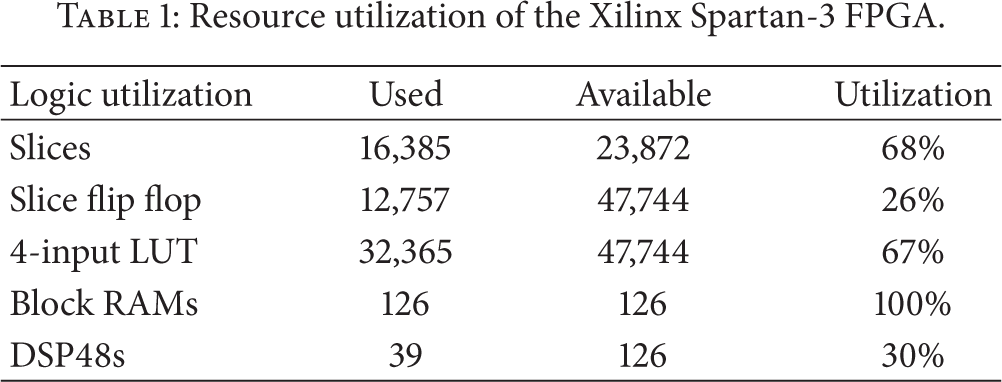
We also tried to achieve a real-time detection while consuming a minimum amount of hardware resource. Table 1 shows the synthesis results and resource utilization of our face detection system based on the logic element of the target FPGA. Considering the essential element like memory for saving the trained data, Table 1 shows that the resource sharing of the logic blocks is fully used to design the proposed face detection system.
Resource utilization of the Xilinx Spartan-3 FPGA.
We could estimate the average of the detection frame rate using the obtained clock frequency from the synthesis results. The performance evaluation presented in this section is based on the combination of the circuit area and the timing estimation obtained from Xilinx's evaluation tools and Mentor Graphics design tools, respectively. Table 2 summarizes the design features obtained from our experiments.
Test results for target FPGA platform.

To estimate the performance of the proposed face detection system, we processed all input images continuously to measure the total number of clock cycles. The system operating at the maximum frequency of 100 MHz processed 200 test images within 4.762 sec, which means the processing rate is estimated to be 42 fps. This result is including actual overhead for switching frames and subwindows. Additionally, the FPGA implementation achieved 96% accuracy of detecting the faces on the images when compared to the OpenCV software, running on the same test images. This discrepancy is mainly due to the fact that the OpenCV implementation scales the features up which does not result in data loss. However, our implementation scales down the frame image instead of feature size during detection process. Another reason for the above difference is that the FPGA implementation used the fixed-point arithmetic to compute floating point number, which essentially has a precision loss.
A direct quantitative comparison with previous implementations is not practical because previous works differ in terms of targeting devices and the need for additional hardware or software. Moreover, some conventional works did not open their detailed data for their implementation. Although the target platform is different in its design purpose, we believe that it is enough to show the rough comparison with previous designs.
Table 3 presents the comparison of the proposed design between previous works focused on low-cost face detection. The implementation of Wei et al. [27] has the same design strategy with the proposed design in terms of compact circuit design. In general, the major factors for evaluating the performance of the face detection system are the input image size, the stage number, and the feature number of the classifier. The image size has a direct effect on the face detection time. Therefore, the bigger image size requires the longer processing time. Although we use four times larger input image than the implementation of Wei et al. [27], our architecture is about 3 times faster. Due to the nature of the cascade structure, the speed of a face detection system is directly related to the number of stages and to the number of features used for the cascaded classifier. The smaller number of stages or of features used in the classifier gets the faster detection time. However, in the inverse proportion to the fast speed, the accuracy of face detecting will decrease. From this point of view, the experimental results showed outstanding performance of the proposed architecture for face detection compared to that of [27, 28]. As a result, we can say that the uniqueness of our face detection system is that it supports real-time face detection on embedded systems, which urge for high-performance and small-sized solution using low-price commercial FPGA chip.
Comparisons between the proposed design and the previous works for low-cost face detection.

5. Conclusion
This paper proposed a low-cost and efficient FPGA-based hardware architecture for the real-time face detection system applicable to an analog video camera. We made an effort to minimize the complexity of architecture for integral image generator and classifier. The experimental results showed that the detection-rate of the proposed architecture is around 96% of that of OpenCV's detection results. Moreover, the proposed architecture is implemented on a Spartan-3 FPGA as an example of practical implementation. The results of practical implementation showed that our architecture can detect faces in a 320 × 240-pixel image of analog camera at 42 fps with the maximum operating frequency of 100 MHz. Considering the balance between the hardware performance and the design cost, the proposed architecture could be an alternative way of a feasible solution for low-cost reconfigurable devices, supporting the real-time face detection on conventional analog video cameras.
Footnotes
Conflict of Interests
The authors declare that there is no conflict of interests regarding the publication of this paper.