
Abstract
The electrochemical micromanufacturing process, as a key micromanufacturing technology, plays an important role in diverse industries. In this paper, polydimethylsiloxane (PDMS) is employed as a mask in the electrochemical micromanufacture of microstructures because of its chemical resistance, low cost, flexibility, and high molding capability. A new method for fabricating a PDMS micro through-holes mask is proposed. In this method, a thin resist film is employed to enhance the adhesion between the substrate and the SU-8 pillar array which is used as a mold. A vacuum-aided process is used to inject the PDMS gel into the SU-8 mold and the PDMS micro through-holes mask can be peeled off from the SU-8 mold when the gel is cured. Experiments were conducted to verify the feasibility of the proposed approach and PDMS microholes of various shapes were obtained. The PDMS mask can then be successfully applied in the electrochemical micromanufacturing process to generate microstructures and microdimple and embossment arrays have been successfully demonstrated. Furthermore, the PDMS mask can be reused, as it is not damaged during the manufacturing process.
1. Introduction
In the past few years, the fabrication of metallic microstructures has rapidly increased due to demand for different applications such as sensors, medical devices, and micromachines [1–3]. A number of techniques are available for microstructure manufacture, such as mechanical machining, electrical discharge machining, chemical etching, laser-beam machining, and lithography, electroplating, and molding (LIGA) [4].
Electrochemical micromanufacturing is a key micromanufacturing technology that has been used to manufacture microstructures with the advantages of no heat affected zones, no cutting force, and no tool wear [5, 6]. Photolithography, which is employed to produce micropatterns on photoresist-coated workpiece, is a common step in the electrochemical micromanufacturing process [7, 8]. However, the process of photolithography is complex, and the photoresist coating is only a one-time mask and must be removed from the workpiece after micromachining. Moreover, the highly cross-linked photoresist coating is difficult to remove reliably from structures without damage or alteration to the electroplated metal. In order to simplify the process and reduce the costs, a reusable PDMS mask is introduced for electrochemical manufacturing process in this paper.
Based on previous reports, through-hole PDMS layers have been achieved in various ways such as dry etching, laser cutting, the removal of photoresist (PR) posts, and spin-coating. Compared with the others, spin-coating is a simple method which does not require additional equipment, unlike dry etching and laser cutting. However, spin-coating alone is not enough to obtain well-defined holes in the PDMS layer, because there is inevitably a thin residual prepolymer layer on top of the SU-8 mold [9]. To complete the opening of the micro through-holes, additional labor is required to remove this excess PDMS. Choi et al. presented a process for fabricating PDMS micro through-holes by a method of capillary micromolding [10]. In this method, a PDMS master mold with micropillars is cast from a corresponding SU-8 mold. The PDMS mold is then fastened closely to a glass slide and the space between the PDMS mold and the glass slide is filled with PDMS gel by capillary action. However, this process is complex, because two molds are required and both the PDMS mold and glass slide must be treated with atmospheric-pressure CH4/He RF plasma to prevent sticking when the PDMS is cured.
In this paper, a new process for fabricating a PDMS mask with micro through-holes is proposed, in which the PDMS gel is rapidly injected into the channel between the SU-8 mold and the substrate using a vacuum-aided process. After the PDMS is cured, it can be smoothly peeled off from the SU-8 mold and the substrate. Compared with the others, the presented method might fabricate PDMS through-holes mask without expensive equipment and complex processes. Finally, using the PDMS mask, a microstructure array is successfully generated by electrochemical micromanufacturing.
2. Fabrication of PDMS Micro Through-Holes Mask
In this study the PDMS micro through-holes mask was fabricated in two main steps: mold making and molding. BN308-150 negative photoresist (Kempur Microelectronics, Inc., China), SU-8 2050 negative photoresist, and a propylene-glycol-methyl-ether-acetate (PGMEA) developer (MicroChem Corp., MA, USA) were used to fabricate the SU-8 mold. Polished 3 mm thick silicon wafer substrates were cut into 2 in-diameter disks to fit the photomasks. A scanning electron microscope (S3400N, Hitachi, Japan) was used to scan the micro-SU-8 mold.
2.1. Fabrication of an SU-8 Mold with a Micropillar Array
Figure 1 presents a schematic view of the fabrication process for an SU-8 mold with a micropillar array. The details of the step are as follows.

Fabrication process of the SU-8 mold with a micropillar array. (a) Substrate surface cleaning. (b) BN308-150 resist casting and prebake. (c) UV exposure without mask and postexposure bake. (d) SU8-2050 resist casting and prebake. (e) UV exposure. (f) Postexposure bake and development.
2.1.1. Pretreatment of the Substrate
To obtain maximum process reliability, substrates should be clean and dry before the SU-8 resist is applied. First, the silicon wafer substrate is dipped into an acetone solution in an ultrasonic cleaner to remove any oil films or impurities from the substrate surface. This is followed by acid washing and dipping in sodium hydroxide to remove metal ions from the substrate surface. The substrate is then dipped into the acetone solution again to remove any remaining acid or alkali, and, finally, the substrate is rinsed with deionized water and placed on a 150°C hotplate for 15 min to remove any residual water (Figure 1(a)). Then, the silicon wafer substrate surface is coated with a BN308-150 photoresist layer to a thickness of 2.5 μm. The thin photoresist coat on the substrate is baked for 20 min at 90°C and undergoes UV exposure without a mask, followed by a postexposure bake at 130°C for 30 min (Figures 1(b) and 1(c)).
2.1.2. SU-8 2050 Photoresist Coating and Softbake
An SU-8 film is spin coated onto the substrate, which is then placed on a hotplate. The temperature of the hotplate is increased to 65°C, kept constant for 10 min, and then increased to 95°C at 10°C min−1. This temperature is then maintained for 90 min and the substrate is then cooled to room temperature (Figure 1(d)).
2.1.3. Exposure, Postexposure Bake, and Development
UV exposure is carried out on a traditional mask aligner (BG-401, 45th Research Institute of CETC), with a primary wavelength and wave energy of 365 nm and 6 mW cm−2. A postexposure bake process is then carried out on a hotplate: the temperature is held at 65°C for 10 min and then at 95°C for 30 min before it is cooled to room temperature. After the postexposure bake process, the substrate with the photoresist coating is developed using pure PGMEA with gentle ultrasonic agitation for 10 min until the development is complete, which can be checked with isopropyl alcohol. The substrate is then rinsed with deionized water. Lastly, the substrate is baked at 50°C for 10 min to remove any residual water and the SU-8 mold with a micropillar array is complete (Figures 1(e) and 1(f)). SU-8 molds fabricated with various shapes are shown in Figure 2.

SU-8 micromolds.
As shown in Figure 2, SU-8 micropillars are distributed on the substrate, while each pillar is independent. As the contact area is quite small, the micropillars are easily detached from the substrates. In our experiments, micropillars of 100 μm diameter and 300 μm height generated by photolithography with the SU-8 photoresist coated on the substrate fell directly from the substrate, as shown in Figure 3(a). It was found that more micropillars fell from the substrate with a reduction in pillar diameter. This can be explained as the development is nonuniform and completion of development at the edge of the substrate takes less time than in the center, so the micropillars at the edge stayed in the developer for a longer time. Because of the small contact area, the adhesion between the substrate and the SU-8 pillar could not support the pillars for this longer time, leading to the detachment of the pillars. Thus, enhancement of the adhesion between the substrate and the SU-8 pillar is important to avoid the detachment of the micropillars from the substrate during the fabrication of micropillar arrays of small diameter. In this study, a BN308-150 photoresist was employed to enhance the adhesion between the substrate and the SU-8 pillar. Because the thin film coated on the substrate was exposed without a mask before the SU-8 photoresist coating, it remained on the substrate during development. Meanwhile, both BN308-150 photoresist and SU-8 photoresist are resin materials, so the adhesion between the two photoresist layers is much better, so avoiding detachment of the pillars during development. The BN308-150 thin film is employed as glue to enhance the adhesion between the substrate and the SU-8 pillar. Figure 3(b) shows a micropillar array with 50 μm diameter and 300 μm height, generated by photolithography with a thin photoresist film coated onto the substrate. The aspect ratio of the pillar array can be up to 6. It can be seen that the pillar array is perfect, with no pillar detachment. Moreover, at the next step, because of the good adhesion, when the PDMS through-hole mask is peeled off the SU-8 mold, the micropillar array will remain on the substrate, avoiding pillar-blocking of the PDMS micro through-holes.

Micropillar arrays fabricated with and without BN308-150 thin film.
2.2. Fabrication of PDMS Micro Through-Holes Mask
In this study, PDMS gel (Sylgard 170, Dow Corning Corp., USA) was used to replicate the patterns of the mold. The fabrication process for the PDMS micro through-holes is schematically shown in Figure 4. First, double-sided tape was stuck onto the flat substrate 2 (Figure 4(a)). Second, substrate 1 with the micropillar array was aligned with the flat substrate 2 (Figure 4(b)); due to the adhesion and flexibility of the tape, the top of the pillars can be placed on the flat substrate 2 in conformal contact. At this point, the mold for the micropillar array channel is finished. Third, the mold is placed in a container and a PDMS gel composed of a mixture of PDMS base and curing agent at a 1: 1 ratio is poured into the container. Then, to remove the air in the gap between the SU-8 mold and the flat substrate 2, the container with the PDMS gel is placed in a vacuum chamber; thus, the gap is filled with the PDMS gel, as shown in Figure 4(c), and it takes 2 minutes to fully fill the gap with PDMS gel. Finally, the PDMS gel is solidified in an oven at 70°C for 0.5 h. Subsequently, the cured PDMS through-hole mask is smoothly peeled off the SU-8 mold and the flat substrate 2 without any damage (Figure 4(d)). Fabricated PDMS micro through-holes mask with different patterns are shown in Figure 5.

Fabrication process for the PDMS micro through-holes mask. (a) Substrate 2 with double-sided tape. (b) SU-8 mold aligned on substrate 2. (c) The PDMS gel fills the gaps by VAP. (d) The PDMS gel is cured and removed from the mold.

Fabricated PDMS micro through-holes masks.
3. Application of the PDMS Micro Through-Holes Mask in the Electrochemical Micromanufacturing Process
The PDMS micro through-holes mask was employed in the electrochemical micromanufacturing process for a microstructure array. Before being attached to the workpiece, the PDMS mask was submitted to corona treatment for 10 s to improve its adhesive property with workpiece and then the mask was attached to the workpiece with rubber roller laminating machine, as shown in Figure 6. With this method, the PDMS mask can be well attached to the workpicee without structure distortion and bubble trapping issues. Figure 7 illustrates the schematic of the experimental setup, which consisted of a power generator, an electrolytic cell, a temperature control unit, and a magnetic bar. In this setup, the PDMS mask with micro through-holes was placed on the workpiece and the electrolyte was flowed onto the surface of the PDMS mask to fill in the holes in the PDMS. The regions exposed to the electrolyte are eroded when a sufficient voltage is applied. A major advantage of this method is that the PDMS mask, as a polymer material, can be reused because it is not damaged in the manufacturing process.

The process of PDMS mask attached to the workpiece.

Schematic of electrochemical micromanufacturing process with mask.
3.1. Fabrication of Microdimples by ECM with PDMS Mask
In this experiment, the thickness of the mask fabricated with PDMS is 200 μm and the diameter of the array of through-holes in the PDMS is 50 μm. According to the principle of ECM, the workpiece is the anode and the regions of the anode that are exposed to the electrolyte dissolve when a sufficient voltage is applied. The operations were carried out with 20 gl−1 sodium nitrate electrolyte, which was pumped at a pressure of 0.1 MPa, and the applied voltage was 8 V with the interelectrode gap at 2 mm. Figure 8 shows the image of the microdimples with a diameter of 61.5 μm and depth of 3 μm generated by the PDMS mask, which was scanned by SEM and three-dimensional profilometer (DVM5000, Leica, Germany). Using this method, 150 microdimples were prepared in 10 s.

Microdimples machined by ECM with a PDMS mask.
3.2. Fabrication of Microembossments by Electroforming with PDMS Mask
In the same way as PDMS micro through-holes can be used in a through-mask ECM for microdimples, so a PDMS mask with through patterns can be used in the electroforming of microembossments. In this process, when a sufficient voltage is applied, metal ions are deposited onto the exposed regions of the workpiece, which acts as a cathode. In the experiments, acid sulfate copper solution was used as the plating solution, with the composition: 240 gl−1 CuSO4·5H2O, 60 gl−1 H2SO4, and 30 mgl−1 NaCl. All the experiments were carried out at a temperature of 30°C and a current density of 1.5 A dm−2.
As shown in Figure 9, a metallic microstructure array of crosses was fabricated successfully with a PDMS mask, the wall-to-wall width of the cross structure is 100 μm and the height is 25 μm (see Figure 9(b)).
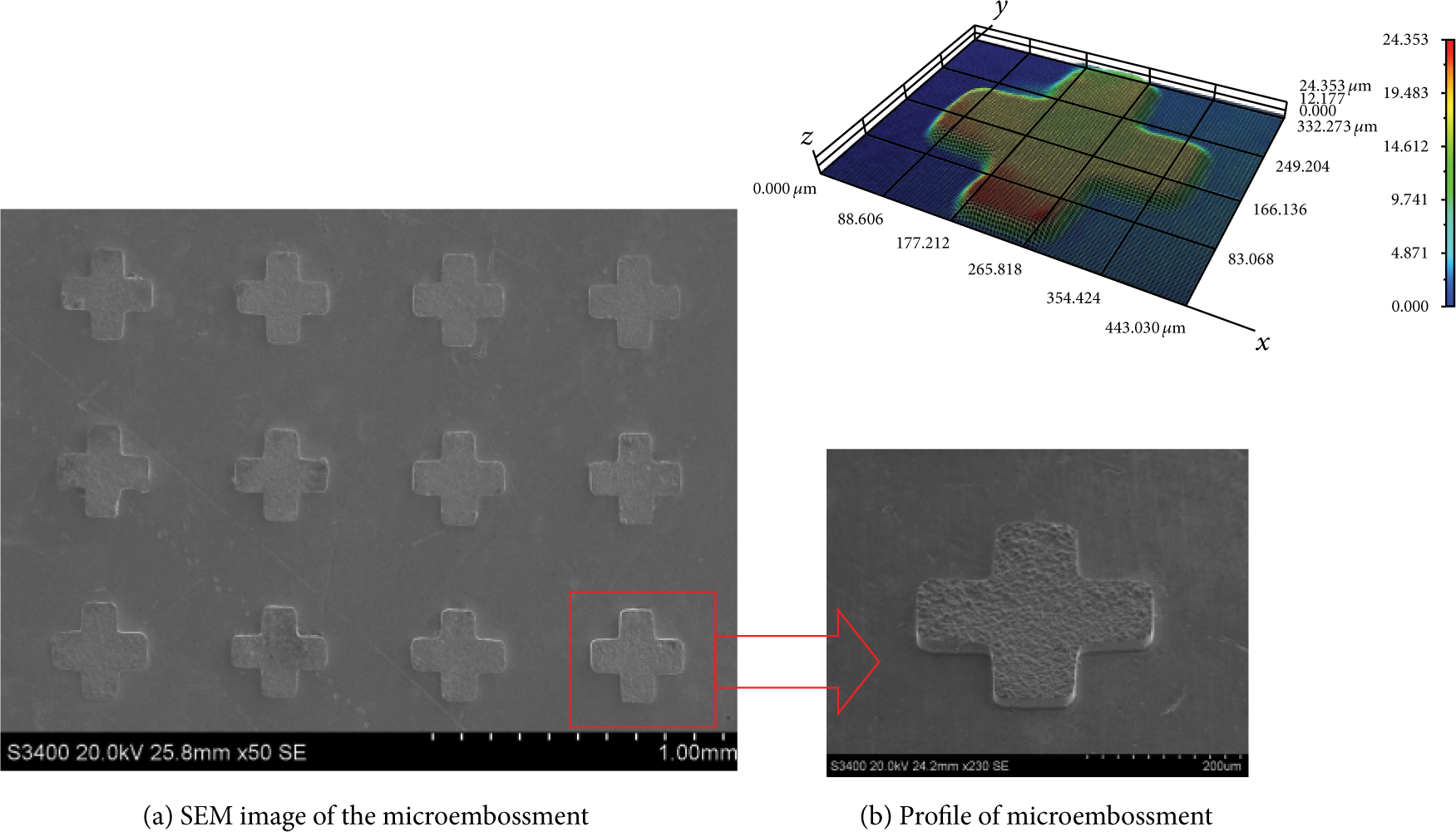
Microembossments produced by electroforming with PDMS mask.
4. Conclusions
A new fabrication process for PDMS micro through-holes mask for generating a microstructure array has been demonstrated. Based on the experimental investigations, conclusions can be summarized as follows.
PDMS micro through-holes of various shapes can be fabricated easily by this presented method and the minimum diameter of the hole can be 50 μm.
A PDMS mask can be used in ECM for preparing a microdimple array and dimples with a diameter of 61.5 μm and depth of 3 μm were successfully generated.
A PDMS mask can also be employed in microelectroforming; a micro-cross-embossment with a width of 100 μm and a height of 25 μm was also successfully generated.
Conflict of Interests
The authors declare that there is no conflict of interests regarding the publication of this paper.
Footnotes
Acknowledgments
The work described in this study was supported by the Joint Funds of the National Natural Science Foundation of China and Guangdong Province (Grant no. U1134003), Funding of Jiangsu Innovation Program for Graduate Education (no. CXLX13_142), and the Fundamental Research Funds for the Central Universities.