
Abstract
Since the Field Programmable Gate Arrays (FPGAs) with high density are available nowadays, systems with complex functions can thus be realized by FPGA in a single chip while they are traditionally implemented by several individual chips. In this research, the control of stepping motor drives as well as motion controller is integrated and implemented on Altera Cyclone III FPGA; the resulting system is evaluated by applying it to a 3-axis caving machine which is driven by stepping motors. Finally, the experimental results of current regulation and motion control integrated in FPGA IC are shown to prove the validness.
1. Introduction
Field Programmable Gate Arrays (FPGAs) allow designers to integrate their hardware functions, such as microprocessor, specific hardware circuit, memory block, and external memory controller in a single chip. It is much more cost effective and efficient than implementing each function as a discrete component on a Printed Circuit Board (PCB) or doing it in an Application Specific Integrated Circuit (ASIC) with a growing number of applications. Particularly, due to the increasing availability of software tools and readily available Silicon Intellectual Properties (SIPs), FPGAs are then becoming a more appealing alternative all the time to the hardware design [1].
Stepping motor generally operates on open loop; it does not incorporate feedback but monitors position by keeping track of the number of steps taken from the start position. With fewer components, simpler electronics, and minimal points of failure, stepping motor is easier to install and less expensive than servo motor. However, to make the motor run stably and fast, a robust motor drive is necessary.
Typically, the stepping motor operates on a step-stage sequence; it is just a series of commands that energize phases at set time increments to move the motor in discrete steps rather than continuously. When they are used in motion control system, the operation condition should pay more attention to the possibility of missing steps. V-curve and S-curve are generally considered to make the motor successfully follow a predefined trajectory.
The researches of stepping motor drive design with FPGA could be seen in [2–6]. In [2], the authors use Cyclone II FPGA and two digital-to-analog converters (DACs) to the implementation of microstepping control. The delivery of control signals is through the RS232 interface, and velocity and position profiles are generated by FPGA. In [3], the authors adopt analog-to-digital converter (ADC) to obtain the winding current. And PI controller, which is a 32-bit microcontroller implemented by FPGA, is used to the current regulation. Regarding [4], an integrated system is presented, which focuses on a stepping motor-driven core to achieve the speed control of stepping motor. Hall current sensor and smart IGBT are, respectively, used for current feedback and switches of power converter, and PID controller is designed to the winding current regulation. In [5], the authors use the FPGA to design the control code and operate the stepping motor drive system in microstep to stabilize the output torque. About low cost sensor for the current control, in [6], the authors use the operational amplifier as the interface to the analysis of missing steps of stepping motor. In conclusion, for those researches, current sensors, A/D and/or D/A converters, analog devices, and PI/PID controllers are generally used to the development of drive system, and controllers realized by FPGA chip have been adopted widely.
In general, the motor drive system and motion controller for multiaxis system are two separated units. With the high density and programmable flexibility and the resource of free microprocessor IP, such as 8051, we have constructed an embedded system which integrates motor drive and motion control into one FPGA chip.
In the previous work [7], the routes in G-code are preprocessed by PC, segmented and converted into binary code in step format, and stored to the Universal Serial Bus (USB) flash memory. For this structure, it needs a lot of memory space inside the motion controller to temporarily save those binary control codes for further processing. With that system, the motion controller embedded in FPGA merely runs the multiaxis digital differential analyzer (DDA) functions; its calculation load is light. However, the motion routes (G codes) for the new designed one need not be segmented and converted into binary code in advance, and we use the USB interface to deliver the text codes of route to the embedded microprocessor, which integrates those functions such as current regulation, DDA, and motion control. The stepping motor drive system is thus redesigned based on the previous research [8, 9] and will be shown in Section 3.
This paper is organized in the following manner. Section 2 presents the overview of the stepping motor based caving machine platform. Next, Section 3 demonstrates the integrated design using the FPGA on the motion control and stepping motor winding current regulation. And Section 4 points out the details of the current regulator with flow diagram. The simulated and experimental results of implementing the inner loop current control and outer loop motion control are revealed in Section 5. And finally, the conclusion is given in Section 6.
2. The Stepping Motor-Driven Caving Machine Platform
In the platform, motion controller and multiaxis motor drive system are combined to make the platform work properly. Most of the motion control systems generate the pulse step commands to make the motor drives, which are in position mode, move and follow the desired path. For our system, however, it has the benefit to reach a fast response compared to the general position control mode because the system is completely controlled by the FPGA system; that is, the inner current loop and outer velocity/position control loop are both executed by one FPGA chip, and just two control loops, position/velocity and current, exist.
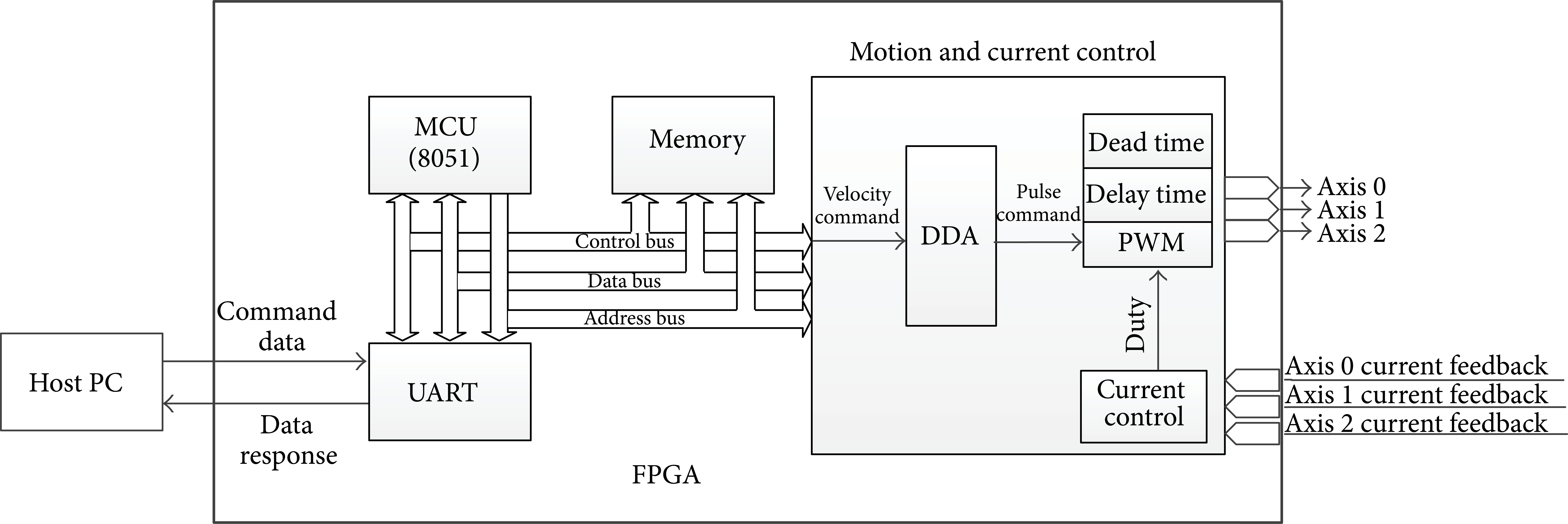
The proposed system includes the following functions: G-code editing and conversion, human machine interface (HMI), FPGA-based motion controller, stepping motor drives, and 3-axis moving platform. Furthermore, the developed system in FPGA IC includes the following components: microprocessor (8051 compatible) based controller, DDA interpolator modules, velocity control with trapezoidal velocity profile, and pulse width modulation (PWM) modules for motor drives. In Figure 1, the block diagram of system structure is shown; it includes the HMI programmed by C language, the PCB boards for motion and current control, power converter realized by MOSFETs and gate drivers, and 3-axis motion platform. The HMI system is illustrated in Figure 2. By it, we could set the resolution of x-, y-, and z-axis, give the start processing command, reset or pause the system, set the system in manual control mode or caving mode, and so on. And Figure 3 demonstrates the appearance of caving machine designed for the research.

The proposed system block diagram.
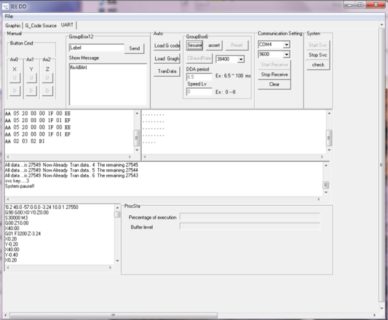
Human machine interface.

The appearance of experimental caving machine.
Due to the step control property of stepping motor and the start-run-stop characters for the application of caving machine, the motor speeds of x-, y-, and z-axis are programmed into four possible values constricted by the trapezoidal velocity profile as shown in Figure 4, where the maximum speed is 180 rpm. To realize the algorithm of trapezoidal velocity profile [10], for each of the point-to-point commands, the maximum motor speed is first decided. In our system, the interrupt time is 6.5 ms, and the corresponding maximum displacement is 4 steps. If the calculated maximum speed is greater than 180 rpm (4 steps in 6.5 ms), it will be restricted to the maximum speed 180 rpm. After that, the acceleration is implemented according to the trapezoidal velocity profile.
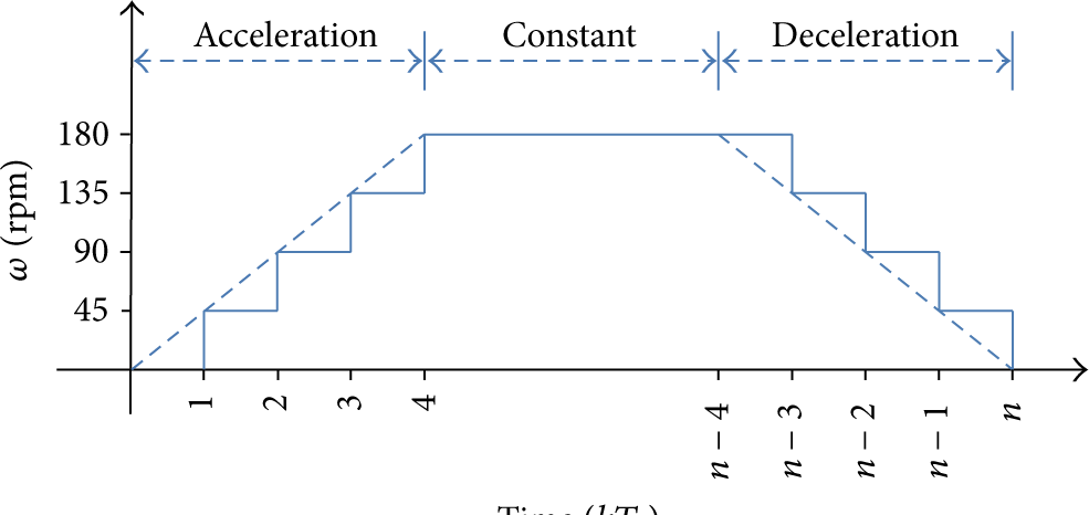
The trapezoidal velocity profile.
3. FPGA-Based Integrated Design for Motor Drive and Motion Control
The integrated system for motion control and motor drive is going to be shown in the following subsections. And Figure 5 is the designed hardware board. The main components shown in Figure 5 are listed in Table 1. FPGA IC is produced by Altera Corp.; USB to UART interface is realized by PL-2303 HXD.
The part description of control board.

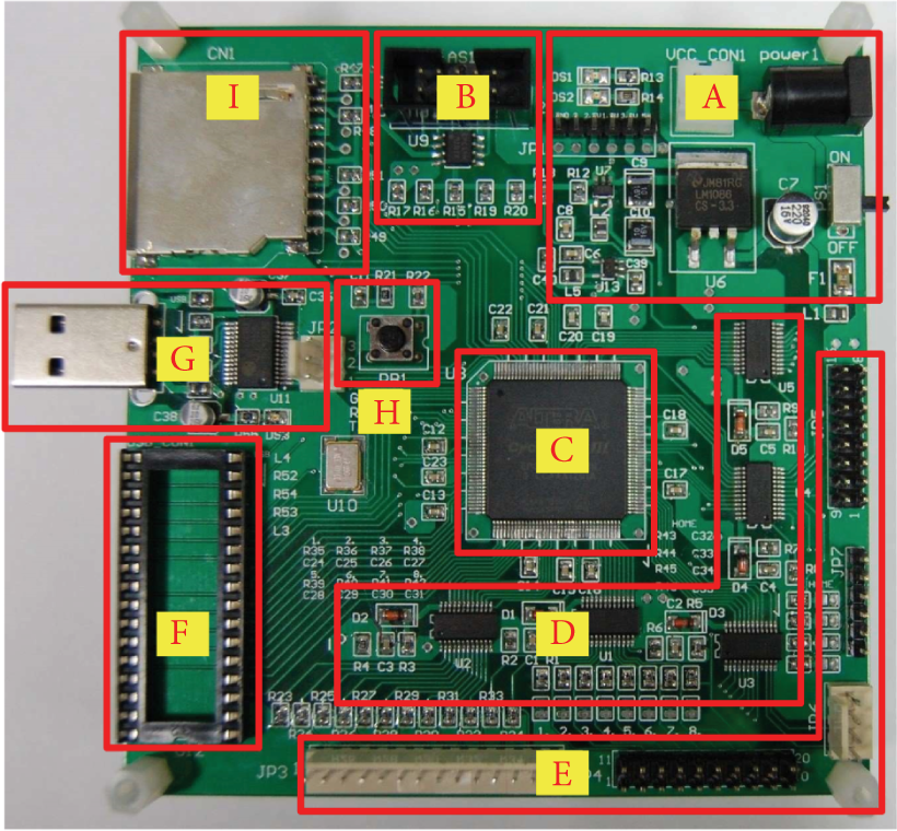
The developed control board.
3.1. Motion Controller Design
To integrate the desired control functions within a chip, they are first digitalized and then realized by the hardware circuit. The operating procedure is initialized from the HMI, which processes the desired routes and converts them into the standard G-code file in text format. The HMI system then sends the motion commands to the motion controller which moves the motors to follow the preprogrammed routes with the constraints of trapezoidal velocity profile and DDA. Figure 6 shows the main blocks of the proposed embedded controller in FPGA.
The block diagram of embedded controller.
3.1.1. 8051 IP Core
For the designed system, the microcontrol unit (MCU) IP core embedded in the FPGA is an 8051 compatible one and includes those associated components: 256 bytes RAM, 8 kB ROM, and 1 kB RAMX for memory extension. The embedded MCU could provide all the functions as a commonly used 8051. It operates at the clock frequency of 24 MHz, and most of the instructions are done in one machine cycle which is designed to be one clock pulse.
3.1.2. DDA Module
DDA algorithm is executed and controlled by the embedded MCU and hardware circuits. The DDA algorithms and signal flow diagram for 3-axis motion control could be found in [8].
3.2. Power Converter of Stepping Motors
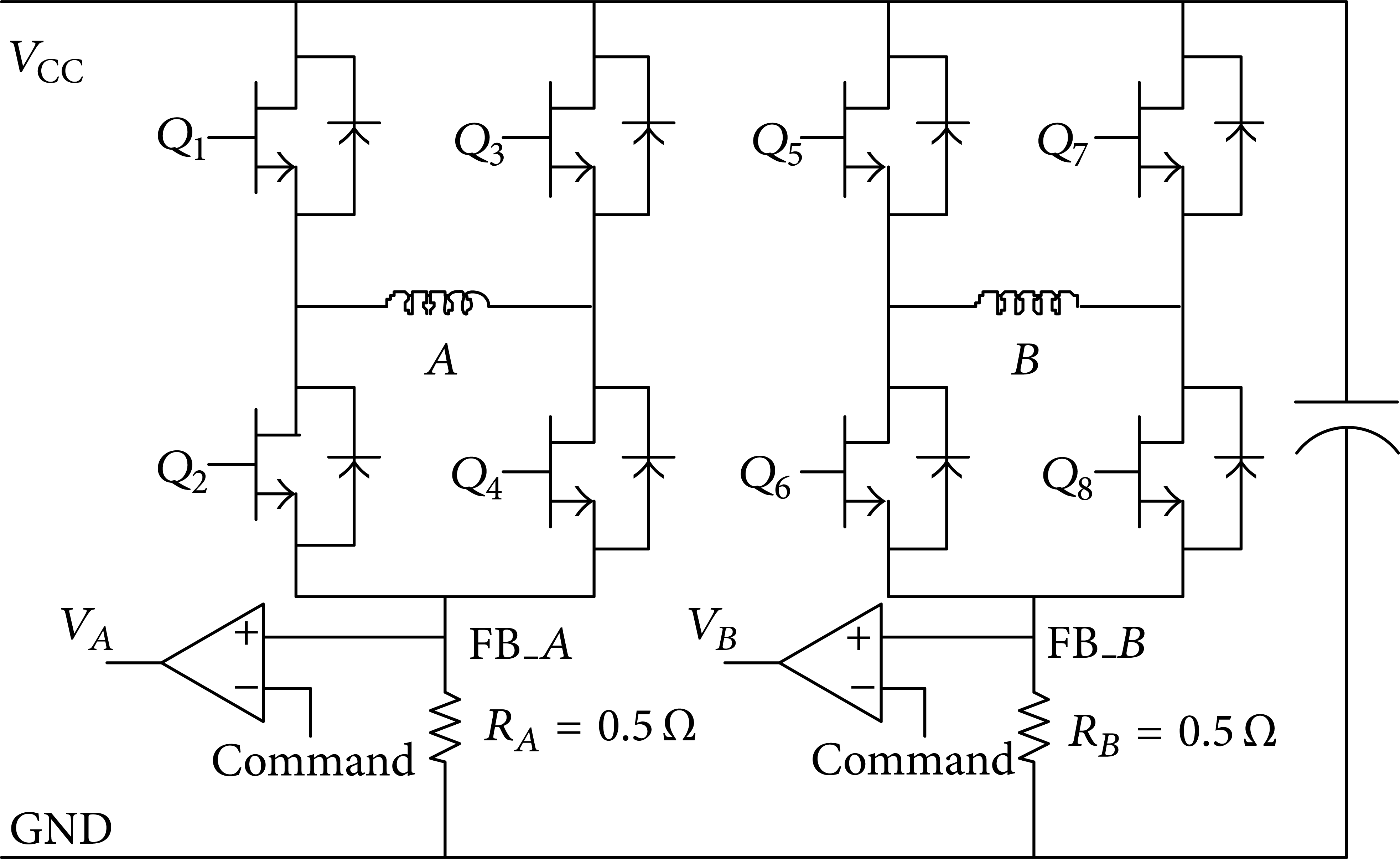
The power converter used to the experiment is shown in Figure 7 with two full bridges and operated in bipolar mode. The switches of full bridges are MOSFET with type IRF640 and driven by IR2101 driver IC. The DC bus voltage is 48 V and current command is set as 0.8 A. The stepping motors are operated in full-step mode.
The power converter of hybrid stepping motor.
In [7], the controller regulated the motor winding current without the feedback of current, and the PWM duty cycle is determined according to the speed command. But for the new designed one, the current feedback of stator winding is achieved with a 0.5 Ω shunt resistor, and the voltage on the resistor is compared with the desired current level by analog comparator. The one-bit comparator's output is then sent to the current controller made by FPGA to determine the duty cycle of PWM.
Figures 8 and 9 show the practical gate driver board and power converter board to deliver DC power to stepping motors.

The Printed Circuit Board of gate driver circuit.

The power converter for stepping motor. (a) Upper side, (b) bottom side.
4. Average Current Regulator Design
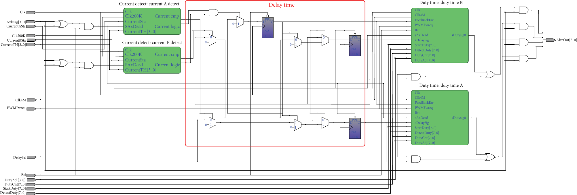
The stepping motor winding current is regulated on the desired level by average current regulating strategy [11]. The hardware circuit is divided into three parts: dead time module, delay time module, and PWM module. Dead time for drive system is set as 1 μs and realized by dead time module, while delay time and PWM modules are used to make the winding current reach the desired level rapidly and keep it consistent until the next phase excitation is coming. The current regulating procedures are as follows: each new step is made; delay time module sets the PWM duty cycle 100% until the magnitude of winding current reaches the desired level. After that, the PWM module hands over and runs consistently to maintain the current on the desired level. The flow diagram of current regulation is shown in Figure 10, and the detailed descriptions are as follows.

The flow diagram of current regulation.
First, the current detector checks whether the current feedback signal exists or not. If no feedback signal (Ifb) is detected, the PWM module then sets the duty cycle to 0%; that is, it turns off the PWM. Second, if the current feedback signal exists, then PWM duty cycle is set to 100% until the winding current reaches the desired level. This is the period of delay time as shown in Figure 11. Third, the PWM module then sets the initial PWM duty cycle to 50% and adjusts the duty cycle according to the average winding current. The upper and lower bounds of PWM duty cycle are set as 80% and 20%, respectively. In this stage, the adjusting procedures are as follows: (1) when the feedback of phase average current is higher than current command, PWM module decreases the PWM duty cycle 1%, and the permitted minimum duty cycle is 20%; (2) when the feedback average current is lower than current command, then PWM module increases duty cycle 1%, and the permitted maximum duty cycle is 80%. To demonstrate how the current regulation and motion control run, the signal flow diagram is shown in Figure 12, where the command is from the HMI interface and accepted by embedded 8051 MCU on FPGA board. 8051 then converts the G-code type commands into pulse-train signals for stepping motor drive system constricted by DDA and PWM modules with sampling time 6.5 ms and 50 μs, respectively. PWM is run in average current mode which has the expected current response in each step as shown in Figure 11. The practical realization to implement the average current regulation is shown in Figure 13. Regarding the step signal module, it is mainly implemented by four D type flip-flops and the sAx0Dir command as shown in Figure 14. Both of the outputs of Figures 13 and 14 are then combined to form the gate driver signals.

The desired waveform of current response.

The step motion flow diagram.
The RTL of ripple of average current regulator.

The circuit of step signal generator.
5. System Setup and Experimental Results
The system to implement the proposed control algorithm is realized on Cyclone III FPGA with the type EP3C5E144C8N, and hardware circuit designs are functional simulated on Quartus II. The following subsections are going to show the performance with the platform stated in Section 2.
5.1. The Verification of Motor Motion Route
The codes used to verify the stepping motor drive system are first generated by CAD/CAM system with G-code format. Figure 15 is the 3D picture of the experimental object, which has the size 40.0 mm in x-axis, 57.2 mm in y-axis, and 13.225 mm in z-axis, and the resolution is set as 0.05 mm. The codes are converted into the amount of steps to be executed, and the total steps in x-axis are 1600 steps, in y-axis 2288 steps, and in z-axis 529 steps. The calculation is according to the stepping motor resolution 200 steps/rev and the lead screw with pinch 5 mm.

The simulated processing object.
5.2. Evaluation of Motor Drive System and Motion Controller
The FPGA-based control system is made to regulate the motor's current to the desired level and simultaneously executes the motion control with DDA algorithm constricted by trapezoidal velocity profile. The codes of route are converted into text file by HMI system on PC and are sent to the motion controller on FPGA by UART interface with baud rate 19600 bps. The maximum motor speed is set as 180 rpm to avoid missing synchronization and is subjected to the constraint of acceleration and deceleration rate. Since the pitch of lead screw is 5 mm, the maximum feed rate is 9 m/min. Additionally, The motor current is fedback through the resistors 0.5 Ω on the power converter, and the current command is 0.8 A.
First, Figure 16 illustrates the simulated PWM signals with constant motor velocity on the condition of DC-bus voltage off. The two command pairs, (A +, A−) and (B +, B−), are complementary for full-bridge trigger signals. It is obvious that those signals are first unmodulated for a short time as the period of delay time shown in Figure 11. Once the stator's current reaches the desired level, the PWM strategy is then activated. Figure 17 shows the relations between the feedback current and the current command. In this figure, CH1, CH3, and CH4 are, respectively, the current comparator output, the current feedback, and the current command. For those experimental results, they are all controlled by the proposed controller integrated in the FPGA chip.

The gate driver signals. CH1: A +, CH2: A−, CH3: B +, and CH4: B−.
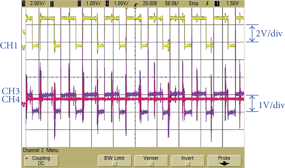
The experimental results of motor drive system. CH1: comparator output, CH3: feedback voltage signal on 0.5 Ω, and CH4: current command.
Regarding the motor drive system design, the experimental results of stator winding currents are shown in Figure 18, which illustrates the current responses at different motor speeds. CH1 and CH2 are, respectively, the MOSFET gate driver signals for phases A and B, and CH3 and CH4 are the corresponding current responses. Comparing these waveforms of Figure 18 with the one shown in Figure 11, they match well. As to the motion controller, the simulated result shown in Figure 15 is processed, and the result is demonstrated in Figure 19; it also fulfills the design.
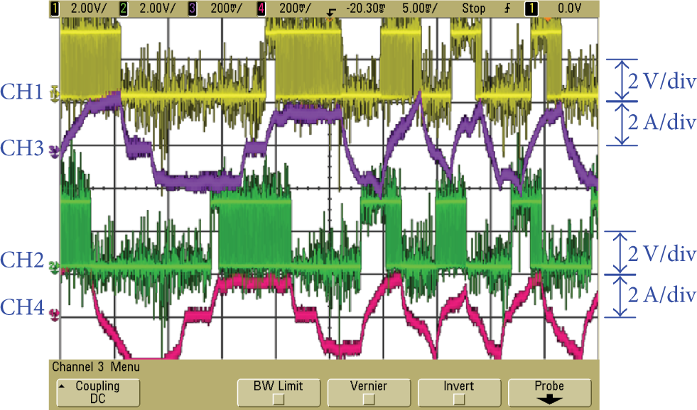
The current responses in different motor speeds.

The processing result of Figure 15.
6. Conclusions
In the paper, we have shown the design by integrating motion controller and motor drive system using FPGA. The motion routes are implemented directly from the corresponding G-codes, which are converted into text format in PC and transferred to the motion controller built in FPGA through the UART interface. The motion controller processes the control codes subjected to the DDA interpolator and trapezoidal velocity profile. Regarding the motor drive system, the winding current is simply fedback by a 0.5 Ω resistor, and the current controller dominated by the strategy of ripple of average current regulates the winding current on the desired level. At last, the developed integrated system is applied to a 3-axis caving machine, and the results, including the current regulation and motion control, successfully prove the validness of the proposed system.
Conflict of Interests
The authors declare that there is no conflict of interests regarding the publication of this paper.