
Abstract
Since hash functions are cryptography's most widely used primitives, efficient hardware implementation of hash functions is of critical importance. The proposed high performance hardware implementation of the hash functions used sponge construction which generates desired length digest, considering two key design metrics: throughput and power consumption. Firstly, this paper introduces unfolding transformation which increases the throughput of hash function and pipelining and parallelism design techniques which reduce the delay. Secondly, we propose a frequency trade-off technique which can give us a scope of frequency value for making a trade-off between low dynamic power consumption and high throughput. Finally, we use load-enable based clock gating scheme to eliminate wasted toggle rate of signals in the idle mode of hash encryption system. We demonstrated the proposed design techniques by using 45 nm CMOS technology at 10 MHz. The results show that we can achieve up to 47.97 times higher throughput, 6.31% delay reduction, and 13.65% dynamic power reduction.
1. Introduction
The explosion of e-commerce nowadays boosts the transaction over the internet; thus we have to prevent intruders from accessing the sensitive information. According to this circumstance, we call for higher security level protection. There are many types of modern cryptography, for example, symmetric-key cryptography, public-key cryptography, and cryptographic hash function. Cryptographic hash function is used in almost every modern application, especially in a multitude of protocols, be it as digital signatures for achieving message authentication and integrity protection. For example, hash-based message authentication codes (HMACs) are used in IP security protocol and also in secure sockets layer (SSL) protocol [1].
As we know, some hash functions, such as message-digest algorithm (MD) series (MD4 and its strengthened variant MD5) and secure hash algorithm (SHA) series (SHA-0 and SHA-1), were widely used, however, broken in practice. Considering the potential danger of being attacked for SHA-2, in 2008, the National Institute of Standards and Technology (NIST) has started the NIST hash competition to develop the future hash standard SHA-3 [2].
Although software encryption is becoming more prevalent today, hardware design is the embodiment of choice for many commercial applications and military [3]. Firstly hardware design is much faster than the corresponding software implementation [4]. Secondly, hardware implementation provides physical protection as high level of security [5]. However, higher security level hash function means more complicated gates, and much more information needs higher frequency to improve the efficiency (or throughput). As a result, the power dissipation of hardware design would increase tremendously. This will cause serious problems in hardware systems, such as less reliability, higher energy consumption, and higher device costs. Thus, low power techniques are highly appreciated in nowadays hardware design.
The rest of this paper is organized as follows. Sponge construction and low power methods which are used in this paper will be introduced in Section 2. In Section 3, we analyze the hash function designed by sponge construction and its original hardware implementation, and then unfolding transformation and pipelining and parallelism design techniques used to improve the throughput and delay of hash function are presented. In Section 4, we construct the hash encryption system and introduce two low power techniques, the frequency trade-off technique and load-enable based clock gating scheme. This paper is concluded in Section 5.
2. Background of the Research
In this section, first, sponge construction will be explained. Next, we will introduce two dynamic power reduction methods which are used in this paper.
2.1. Sponge Construction
The idea of sponge construction came from the design of RadioGatún, and its final definition was given at the Ecrypt Hash Workshop in Barcelona [6]. As shown in Figure 1, sponge construction takes arbitrary length input with finite internal state and gives an output of any desired length.

Sponge construction [6].
There are three components in sponge construction [7]:
a state memory; a function of fixed length that permutes or transforms the state memory; a padding function.
The state memory in Figure 1 is divided into two parts: the top section called bitrate of
Sponge construction consists of two processes: absorbing and squeezing. Considering the left part of dash line in Figure 1, called absorbing, firstly, the input message is padded and the state memory will be initialized; secondly, the first
The extent c-bit part which is altered by the input message depends on the fixed length function [7]. The security of hash function, for example, resistance to collision or preimage attacks, relies on this c-bit part. Because of its arbitrarily long input and output sizes, the sponge construction allows building various primitives such as hash function. Keccak hash function, known as the new SHA-3, uses this sponge construction.
2.2. Dynamic Power Reduction Methods
Digital circuits will consume dynamic power in the active mode. There are two sources of dynamic power consumption [8]:
charging and discharging processes of output capacitance; short-circuit current when PMOS and NMOS networks are all ON.
Because the short circuit power is usually less than 10% of total dynamic power [9], the dynamic power consumption which we try to reduce in this paper is referred to as switching power for the rest of this paper. Dynamic power can be explained in (1). Note that f is the clock frequency and

Since the power optimization at RTL has significant impact with reasonable accuracy, RTL is considered as the optimal stage for low power techniques [8]. According to (1), four parameters, such as voltage, clock frequency, load capacitance, and the toggle rate of gate output, determine the dynamic power consumption. Because reducing supply voltage will increase critical path delay and changing the capacitance of gate output needs to redesign the load logic, it is more efficient to focus on clock frequency and toggle rate at RTL.
2.2.1. Dynamic Voltage/Frequency Scaling
Figure 2 gives us a basic dynamic voltage/frequency scaling (DVFS) system. The DVFS controller will determine the clock frequency, which is sufficient to finish work and gives the best performance without overheating by collecting information about the workload and the temperature. Then this variable clock frequency scheme will lead to dynamic power reduction by choosing proper clock frequency.

DVFS system [9].
2.2.2. Load-Enable Based Clock Gating
As we all know, combinational clock gating technique is widely used to solve dynamic power issue for single level register. And sequential clock gating method considers multiple level (pipeline) registers. In this research, we focus on the combinational clock gating technique; particularly, we use load-enable based clock gating scheme [10].
Figure 3 shows a normal structure of load-enable based clock gating scheme. As we know, if the data do not change during some consecutive clock periods or the enable signal is kept low, those clock periods are wasted. This technique can be applied to a circuit with mux in which an enable signal is a selection signal or a pipeline construction circuit, such as hash encryption system in this research.
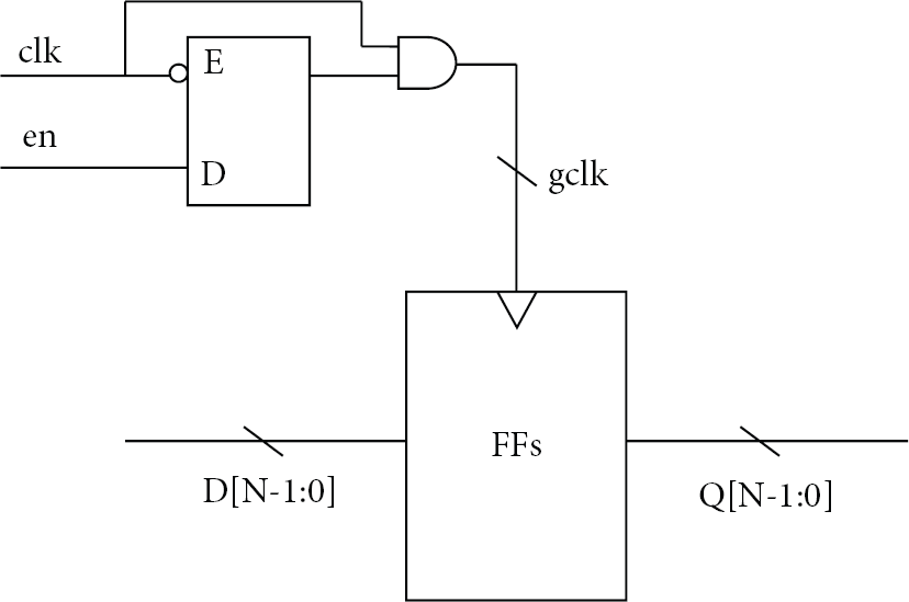
Load-enable based clock gating.
3. Proposed High-Speed Hashing Module in Hardware
Cryptographic hash function provides powerful protection for data; it has been utilized in the security layer of every communication protocol. However, as protocols evolve, data sizes and communication speeds are dramatically increasing; low throughput of hash function seems to be a bottleneck in these digital communications systems. A promising solution is the hardware implementation on reconfigurable devices which combines high flexibility with the speed and physical security.
Various techniques have been proposed to speed up or to improve the throughput of hash function, for example, unfolding transformation and pipeline and parallelism techniques. In this section, the characteristics which are relevant to the hardware implementation of the hash algorithm will be presented. Then the high-speed hashing methodology module will be introduced based on the delay bound analysis. Then two techniques, such as unfolding transformation and pipeline and parallelism, will be used to optimize the inner logic of transformation rounds.
3.1. Hash Algorithm Specification
In this section, we introduce a cryptographic hash algorithm with sponge construction, called sponge hash algorithm (SHAT). SHAT is a hash function generating 128-/256-/384-bit hash values. According to the hash value length, SHAT can be denoted by SHAT-(
The parameters of SHAT.

3.1.1. G Function
G function of SHAT consists of an S-box and a diffusion layer. S-box is a substitution function that satisfies the confusion property on each 4-bit word. A 32-bit input word W, for example, is divided into eight 4-bit words (
S-box of the G function.

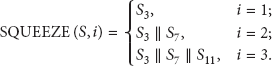
3.1.2. Hash Function of SHAT
SHAT uses the hermetic sponge construction as shown in Figure 4. As we mentioned in Section 2,

Sponge construction of SHAT.
In the absorbing phase, the input message 
Step(S) (i) For (a) (b) (c) (d) (e) (ii) (iii) For (iv)
SHAT-( Inputs: n padded message blocks Outputs: ( (1) (2) Perm(S) (3) For (i) For (ii) Perm(S); (4) (5) For (i) Perm(S); (ii)
3.2. Hardware Implementation
Following the guidelines of SHAT-(

A typical SHAT core.
S-box of G function is designed from Karnaugh map. According to Table 2, we get the logic functions of S-box as shown in (5). We set 
There are 48 iteration rounds in the basic architecture of Perm function. Then we use rolling loop technique to reduce area requirement. Our design is a single operation block which is reused 48 times as shown in Figure 6. Here 
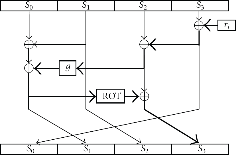
Typical architecture of one STEP round.
3.3. Proposed High-Speed Module
In the previous section, we introduce rolling loop technique to construct Perm function. Although this approach considers area efficiency, throughput is kept low due to the requirement of 48 clock cycles to generate the result. There are many architectures that can be made by varying the Perm function to solve this problem. We performed the unfolding transformation technique. This high-speed module combines STEP blocks into a single round and even can take advantage of architectures with complete round-unrolled circuit. By unfolding, the hidden concurrencies can be parallelized [12]. Also in [13], the pipeline and parallelism technique was explained to improve the unfolding construction of hash function. This technique is related to precomputing by analysing the inner logic and architecture of hash function.
3.3.1. Unfolding Transformation
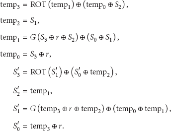
According to Figure 6, the mathematical expression of one iteration round is described as


3.3.2. Pipeline and Parallelism
We assume to unroll two STEP operations in each round; for sure it will reduce the frequency to increase the throughput. However, the increased area is introduced as penalty. If some logics can be done in parallel, and this parallelism happens in critical path, then the delay of each round could be decreased, so that the frequency of each operation will be increased. According to (8), when the number of operations is kept as constant (the number of bits is also kept as constant), the throughput will increase with its frequency. This method could be used in any other hardware implementation of hash function.
For example, Figure 7 shows the architecture of unfolding two STEP operations in one round, which has the minimum critical path delay. The critical path is composed of seven XOR gates and two G functions. By unfolding two STEPs in one round, we have a gain of three 32-bit XOR gates and one G function in critical path comparing with the architecture of one STEP block. The critical path is highlighted by bold line.
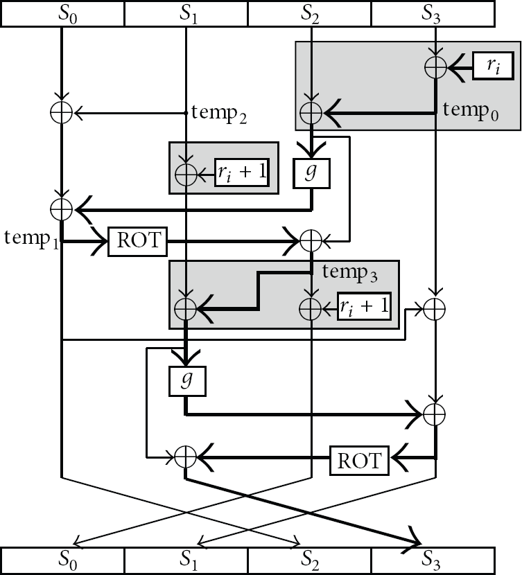
Proposed architecture of two STEPs round.
In Figure 7, cycle counter
Thus, when we increase the number of unfolding STEP operations, for example, three, four, five, …, each round delay will increase by three 32-bit XOR gates and one G function. Therefore, the normalized delay with unfolding factor n (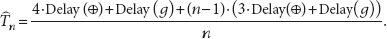

3.4. Experimental Results
We introduce a measurement of hardware efficiency in (12) [14]. This is the improvement of normal figure of merit (FOM). We assume that the power is proportional to the gate count; then we could divide the metric by another GE instead of power dissipation when we want to trade off throughput for power. Note that one gate equivalent (GE) is equal to the area of two-input NAND gate in 45 nm CMOS technology:

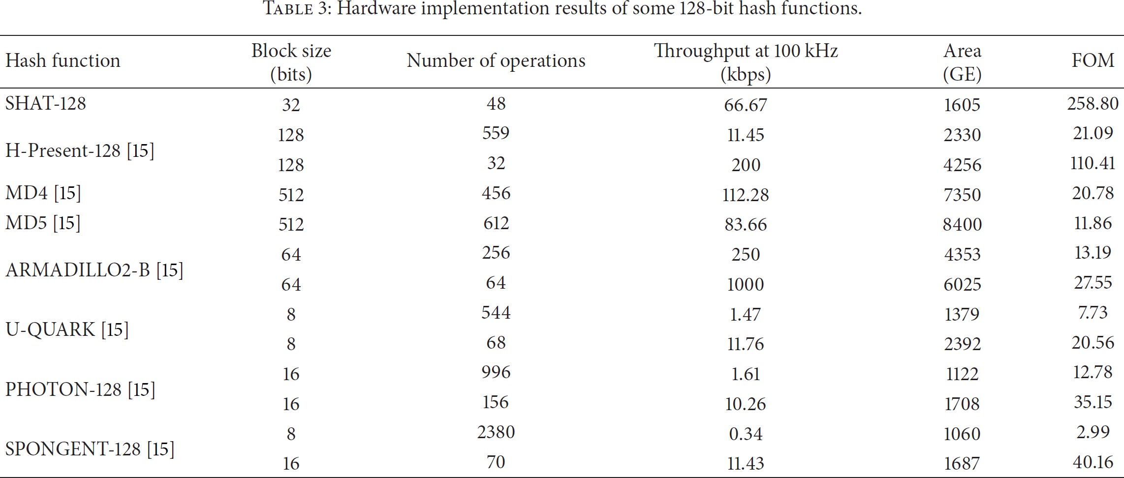
Table 3 shows the hardware implementation results of some 128-bit hash functions by using 100 kHz clock frequency and 45 nm CMOS technique. Firstly, the throughput of SHAT-128 (66.67 kbps) is less than that of other 5 hash algorithms, such as MD4 (112.28 kbps), MD5 (83.66 kbps), H-Present-128-32-round (200 kbps), and ARMADILLO2-B (250 kbps and 1000 kbps). However the area of SHAT-128 is only 28.42% of that of hash functions in average. This results in having the hardware efficiency of SHAT-128 to be 13.12 times higher in average. Secondly, the area of SHAT-128 (1605 GE) is larger than that of 3 hash algorithms, for example, U-QUARK-544-round (1379 GE), PHOTON-128-996-round (1122 GE), and SPONGENT-128-8-bit-2380-round (1060 GE); however, the throughput of SHAT-128 is 94.27 times higher. Thus the FOM of SHAT-128 is 46.75 times higher in average. Finally, the area of SHAT-128 (1605 GE) is less than that of other 4 hash algorithms, for example, H-Present-128-559-round (2330 GE), U-QUARK-68-round (2392 GE), PHOTON-128-156-round (1708 GE), and SPONGENT-128-70-round (1687 GE). And the throughput of SHAT-128 is also 5.95 times higher than that of 4 hash algorithms in average. This results in having the FOM of SHAT-128 to be 9.66 times higher in average.
Hardware implementation results of some 128-bit hash functions.
In Table 4, firstly, the throughput of SHAT-256 is 51.05% of that of Grostl; however, the area of SHAT-256 is only 21.84% of that of Grostl; this results in having 84.47 times higher hardware efficiency of SHAT-256. Secondly, the throughput of SHAT-256 (3193 GE) is 412.91 times higher than that of 2 hash algorithms, such as PHOTON-256-156-round (2177 GE) and SPONGENT-256-9520-round (1950 GE), in average; although the area of SHAT-256 is larger, the FOM of SHAT-256 is still 158.25 times higher than that of 2 hash algorithms. Thirdly, comparing with SHA-256, ARMADILL02-E, BLAKE, PHOTON-256-156-round, and SPONGENT-256-140-round, the throughput of SHAT-256 is 4.65 times higher in average, and the area of SHAT-256 is only 49.15% of that of hash algorithms, in average. Therefore, the FOM of SHAT-256 is 119.14 times higher in average.
Hardware implementation results of some 256-bit hash functions.

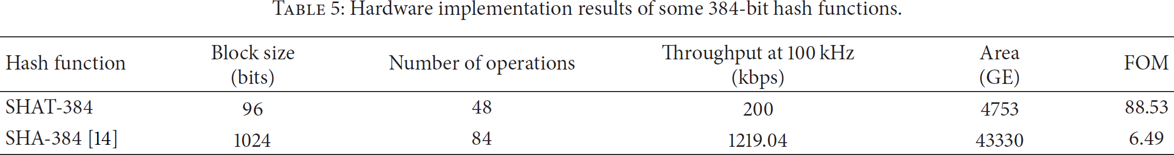
In Table 5, the throughput of SHA-384 is 6.09 times higher than that of SHAT-384; however, the area of SHA-384 is 9.11 times higher; this results in having the hardware efficiency of SHAT-384 to be 13.64 times higher than that of SHA-384.
Hardware implementation results of some 384-bit hash functions.
Then we implement unfolding transformation technique with 10 different numbers of unrolling loops (
Finally we implement pipeline and parallelism technique to reconstruct STEP block, as shown in Table 6; comparing with the performances of original circuit, the critical path delay reduces to 6.31% at most, while the power and area will increase in 8%.
Performance results of hash function using pipeline and parallelism.

Performance results of unrolling steps constructions.

4. Low Power Design for Hash Function
Low power design is a significant consideration in hardware implementation. How much the power consumption is will determine a device's life, reliability, and energy cost. Thus low power technique is applied normally to every application nowadays. There are many methods to reduce power consumption such as clock gating and power gating related to dynamic power and leakage power. Frequency decreasing technique will pull down the power dissipation dramatically as well.
Firstly, we will propose the frequency trade-off technique. By using this method we could achieve a range of frequency values for making a trade-off between low power consumption and high throughput of hash function. Secondly, we construct a hash encryption system which includes input data padding unit, RAM registers, main hash computing construction, message digest extraction component, and main control unit. Thirdly, by analyzing the idle mode and control signals of this hash encryption system, load-enable based clock gating scheme is applied to reduce the dynamic power consumption.
4.1. Frequency Trade-Off Technique
According to (1), reducing clock frequency is an effective method to decrease dynamic power dissipation linearly. In Section 2.2, we talked about the DVFS technique. By collecting the information about workload and temperature, DVFS will determine the sufficient clock frequency for the proper performance. However, modifying the clock frequency at RTL is not easy. Normally, we treat the clock frequency as constant. Also as we know, dynamic frequency scaling reduces the number of operations a system can issue in a given amount of time, thus reducing performance. Therefore, there is an issue we need to consider: high clock frequency brings high level throughput; however dramatically increased dynamic power consumption is the critical drawback. Low clock frequency minimizes the dynamic power dissipation; however it decreases the throughput as well.
However, according to the unfolding transformation technique which is introduced in Section 3.3, the maximum frequency of Perm function will decrease, while the number of unrolling loops increases. It means that we can decrease the clock frequency while increasing throughput of the hash algorithm. Thus, this unrolling transformation technique compromises high performance without high clock frequency. According to this advantage, by choosing proper clock frequency, we can make a trade-off between high performance and low power consumption.
Next, we explain how to get this scope of frequency value from the two performance bounds. For example, first we achieve two values of rolling Perm circuit: dynamic power consumption 
This method can be defined as the following: referring to the performance of original folding circuit (we assume that this circuit is the one with 48 iteration rounds in one Perm function), each unfolding transformation design with different numbers of unrolling STEPs (
This clock frequency scope gives us many different choices for different circuit designs by using unfolding transformation technique. The results of this frequency trade-off technique are shown in Table 9 in Section 4.4.
4.2. Hash Encryption System Design
The hash encryption system is divided into 5 main parts as shown in Figure 8.

Hash encryption system.
Firstly, the receiver and RAM section is actually our padding unit. We use serial communication technique to connect PC and the hash encryption system. Thus, we need clock divider to generate proper clock cycle to be synchronous with Baud rate of serial communication. We choose 4800 Baud/s as our transmission Baud rate which is not a quick speed for low error rate (less than 3%). In this case, one Baud represents 1 bit. Our rule of transmission is a one start bit “0”, then 8-bit message, and one finish bit “1”. This start bit and finish bit will be added into the transmission message bits automatically; the sampling rate of receiver is 16 and FPGA board provides 100 MHz clock frequency. Thus, the clock period used in sampling is 1302 times provided 100 MHz clock period as shown in (14). This error is 0.0064% less than 3%:

Secondly, hash function which we introduced in Section 3 is designed as sponge construction as shown in Figure 4. Absorbing n 32-bit message blocks, there are 128 bits digest that will be squeezed out.
Finally, the main control unit is designed for managing the working order between receiver, hash process, and LCD display. Figure 9 shows the pipeline working of system.

Three phases of hash encryption system.
Because we use serial communication technique, the speed will be slow. We apply 4800 Baud/s as our Baud rate for low error rate; thus each 32-bit block needs roughly 7 ms. For example, there are seven 32-bit blocks that need to be transmitted; roughly 50 ms needs to be dissipated for data receiving and padding. Although the hash function that we used in this system is one STEP each round, this means that there are 48 iteration rounds for a complete Perm function. However, hash processing just needs roughly 6 μs. It also costs much time in LCD displaying period. Even though we can finish LCD initialization before we get hash digest, we still need roughly 1.5 ms to completely display all data.
4.3. Load-Enable Based Clock Gating
In this section, we introduce the load-enable based clock gating technique for the hash encryption system.
Clock gating is the most widely used low power technique at RTL. It is more reasonable to determine the toggle rate of gate output at RTL than any other three components, such as
As shown in Figure 10, there are three signal pairs to realize this load-enable based clock gating:

Control signals of hash encryption system.
Figure 9 gives us three operation phases of the encryption system. In first phrase,
During the second phase, because the padded message is ready, then
This system will enter the third phase when the
By analyzing the construction and process of hash encryption system, we can figure out the idle time for each component. Then applying the load-enable based clock gating to each component, the dynamic power dissipation of this system can be properly reduced as shown in Table 8 in Section 4.4.
Hardware implementation with/without load-enable based clock gating.

Area and delay performances of frequency trade-off technique.

4.4. Experimental Results
By using 10 MHz clock frequency and 45 nm CMOS technology, the results of frequency trade-off technique are shown in Tables 9, 10, and 11. Table 9 shows that the area and critical path delay are not changed comparing with the unfolding transformation technique. Tables 10 and 11 give us the variation of dynamic power consumption and throughput with frequency trade-off method. Note that
Dynamic power consumption of frequency trade-off technique.

Throughput performances of frequency trade-off technique.

Then we apply load-enable based clock gating scheme to hash encryption system by using 100 MHz clock frequency, which can be provided on FPGA board, and 45 nm CMOS technology. As shown in Table 8, the dynamic power decreases 13.65%. However, 3.64% increased area and 5.52% increased critical path delay are sacrificed.
5. Conclusion
In order to achieve high performance and low power hardware implementation for cryptographic hash function which uses sponge construction, firstly, we use unfolding transformation technique to improve the throughput of hash function; secondly, pipeline and parallelism design techniques are implemented to reduce the critical path delay by modifying the structure of permutation function; thirdly, frequency trade-off technique is proposed to calculate a frequency scope which can be used to make a trade-off between low dynamic power consumption and high throughput of hash function; finally, load-enable based clock gating scheme is applied in hash encryption system to eliminate wasted toggle rate of signals in the idle mode.
The experimental results have shown that unfolding transformation technique can achieve up to 47.97 times higher throughput, pipeline and parallelism methods give 6.31% delay reduction, load-enable based clock gating scheme decreases 13.65% dynamic power consumption, and frequency trade-off technique shows how to decide the clock frequency of the hash function to achieve low power consumption and high throughput.
Footnotes
Conflict of Interests
The authors declare that there is no conflict of interests regarding the publication of this paper.
Acknowledgment
This research was supported by the MKE (The Ministry of Knowledge Economy), Korea, under the ITRC (Information Technology Research Center) support program (NIPA-2012-H0301-12-3007) supervised by the NIPA (National IT Industry Promotion Agency).