
Abstract
This study used ANSYS simulation software for analyzing an ultraviolet (UV) (355 nm) laser processing system. The laser apparatus was used in a stainless steel CIGS solar cell P2 layer for simulation analysis. CIGS films process order according to S i O2 layer, molybdenum electrode, CIGS absorbed layer, CdS buffered layer, i-ZnO penetrate light layer, TCO front electrode, MgF resist reflected materials, andelectrode materials. The simulation and experimental results were compared to obtain a laser-delineated P2 laser with a low melting and vaporization temperature. According to the simulation results, the laser function time was 135 μs, the UV laser was 0.5 W, and the P2 layer thin films were removed. The experimental results indicated that the electrode pattern of the experiment was similar to that of the simulation result, and the laser process did not damage the base plate. The analysis results confirm that the laser apparatus is effective when applied to a stainless steel CIGS solar cell P2 layer.
1. Introduction
Membrane process acts the important role that raised the efficiency and lowered costs of solar cell material. In the future, we should understand membrane material to apply to solar cell technology. CIGS film solar cell P2 layer used mechanical process. Advantages of laser processing included fast process, small processing line width, and less edge fragments. Lin et al. [1] described a simple and inexpensive synthetic method that can be used to prepare soluble nanoscale triphenyl phosphine-coordinated CIGS (TPP-CIGS) photoactive functional materials. Nerat [2] used a simple model in which only columnar grains (and GBs) are considered as a 2D approximation of real 3D grains. The simulation results of the CIGS cells of various shapes and sizes of grains may differ from the study presented by Amin et al. [3] who applied numerical simulations of CIGS solar cells with an ultrathin absorber layer to investigate the performance of ultrathin CIGS solar cells. Matsusaka and Watanabe [4] examined the laser machinability and optical absorption of the silver-containing region of CIGS solar cells and presented simple micro-applications.
Chen and Darling [5] determined that the laser ablation process of these materials could be a mix of photothermal and photochemical processes when a near-nanosecond pulse laser is used. However, the ultraviolet (UV) (355 nm) laser micromachining process appears to be dominated by a photothermal process, in contrast to the mid-UV (266 nm) laser. Dai et al. [6] observed that the heat-affected zone (HAZ) is extremely small, and the 157 nm laser etching of GaN epilayers is dominantly a photochemical procedure. Lee et al. [7] measured CIGS films and crater morphologies during Nd:YAG laser (1064 nm) irradiation and determined that strong surface evaporation is dominant for low-Ga concentrated films of which the bandgap is well below the photon energy. Shen and Lin [8] prepared Cu(In, Ga)Se2 (CIGS) thin films on bilayer Mo-coated soda-lime glass by printing with mixed powders of a CIGS quaternary alloy (average partial size of 680 nm) and NaF.
The current study used ANSYS simulation software for analyzing the UV (355 nm) laser processing system. The simulation results confirmed that the laser apparatus is effective when applied to a stainless steel CIGS solar cell P2 layer.
2. Experimental Principle and Details
ANSYS software is a structural, fluidic, electric magnetic field, acoustic field, and coupling field finite element analysis software. This study used this software to analyze a hot-field simulation of a CIGS film solar cell laser delineating a P2 layer material. Figure 1 illustrates the laser process route.

Illustration of laser process route.
The UV laser primarily involves applying a high accuracy microelectronic product, semiconductor, LED, and LCD process. Figure 2 shows a UV laser processing machine. A stainless steel glass base plate was used in this study. CIGS films process order according to S i O2 layer, molybdenum electrode, CIGS absorbed layer, CdS buffered layer, i-ZnO penetrate light layer, TCO front electrode, MgF resist reflected materials, and electrode materials. Figure 3 presents a diagram of the laser solar cell film. The diagram included P1, P2, and P3 layer for solar cell film materials:

where q″ is the thermal current density (W/m-°C), k is the material heat conduction coefficient (W/m2), h is the convection coefficient, T s is the solid surface temperature, T∞ is the surrounding fluid temperature, q is the heat flow rate, ε is the microradiation rate, A1 is the area of radiation surface, F12 is the shape coefficient of the radiation surface, σ is the Stephen coefficient 5.67 × 10⁻⁸ W/m2 k4, and T1 and T2 are the absolute temperatures of the radiation surface.
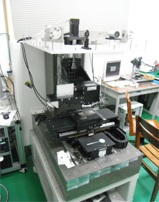
UV laser processing machine.

Diagram of the laser solar cell film.
3. Study Procedure
Figure 4 presents a flow diagram of the experiment. In this study, a UV (355 nm) laser was applied to CIGS solar cell film molybdenum layer processing. The experimental procedure was divided into four major stages. The first stage involved examining the laser characteristic. The machine platform is researched and developed by author's laboratory. At the second stage, sputtering was used to produce an experimental specimen. At the third stage, ANSYS software was used to analyze the hot-field simulation. At the fourth stage, a laser was used to delineate molybdenum electrodes. Moreover, it changed different energy, laser scan speed, laser pulse frequency, and so on.
Flow diagram of experiment.
Table 1 presents the physical parameters of the P2 layer materials. The experimental material film thickness of S i O2 was approximately 300 nm, CIGS was approximately 800 nm, CdS was approximately 50 nm, i-ZnO was approximately 90 nm, and the stainless steel thickness was 1.0 mm.
Physical parameters of P2 layer materials.

4. Results and Discussion
Because the material absorption rate influences the hot-field simulation analysis result, the P2 material absorption rate must be determined first. This study used a stainless steel base plate and no penetrating material. Figure 5 presents the reflection rate curve graph of the P2 layer obtained using a UV-Vis-NIR spectrophotometer. When the simulation reached a wavelength of 355 nm, the P2 layer obtained a reflection rate of approximately 17.95%. The following equation can be used to determine the absorption rates of the P2 layer material:

where A is the material absorption rate (%), R is the reflection rate of the material (%), and T is the penetrating rate of the material (%).

Reflection rate curve graph of P2 layer.
The simulation analysis involved applying a thickness of 1 mm and a width of 2 mm in the 2D net model. The 1 mm × 2 mm mesh area was divided into 20000 grids. When the simulation reached a wavelength of 355 nm, the P2 layer obtained a reflection rate of approximately 17.95% and a material absorption rate of approximately 82.05%. Because the UV laser source focus has a high energy density, the energy selection applied was 0.5 W, the laser light spot diameter was 100 μm, the laser pulse time was 135 × 10−6s, and the initial temperature was 27°C. Figure 6 presents the P2 material's sectional hot-field simulation analysis of the UV laser with a laser power of 0.5 W. The maximal temperature of the material surface reached 2795°C at 0.5 W, enabling the P2 layer material to reach gasification temperature. The melt depth is 0.95 μm. The simulation process is sound and valuable compared with experiment.

P2 material's sectional hot-field simulation analysis of UV laser (laser power 0.5 W).
This study used a 3D confocal microscope to measure the laser etching sizes. Figure 7 presents various energy densities etched on the P2 film by the UV laser obtained using a 3D confocal result microscope with laser energy levels of (a) 0.3 W, (b) 0.4 W, (c) 0.5 W, (d) 0.6 W, and (e) 0.7 W. The observed thicknesses and depths were (a) W = 66.571 μm, h = 0.87 μm; (b) W = 65.62 μm, h = 0.978 μm; (c) W = 65.62 μm, h = 1.002 μm; (d) W = 68.473 μm, h = 1.018 μm; and (e) W = 69.424 μm, h = 1.193 μm. When there is low laser energy, that edge straight scribing is not a complete line. When the laser energy was increased to 0.6 W, the straight line was etched. The S i O2 penetrated the bottom when the laser energy reached 0.7 W.

Various energy density scribe P2 films of UV laser using 3D cofocus result microscope. (a) Laser energy 0.3 W, (b) laser energy 0.4 W, (c) laser energy 0.5 W, (d) laser energy 0.6 W, and (e) laser energy 0.7 W.
Figure 8 presents the molybdenum film UV laser scribes in the 3D microscope analysis obtained using a laser power of 0.05 W. When the laser power was 0.05 W, the depth of the P2 layer material was 0.975 μm, and its thickness was 950 nm; thus, the P2 layer was removed and did not exceed the S i O2 thickness. The analysis process is similarly effective and of value in comparison with literature.
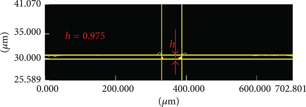
Molybdenum film UV laser etchings in the 3D microscope analysis (laser power 0.5 W).
5. Conclusions
This study used ANSYS simulation software for analyzing a UV (355 nm) laser processing system. The laser apparatus was used on a stainless steel CIGS solar cell P2 layer to simulate the analysis, revealing the following. (1) The maximal temperature of the material surface reached 2795°C with the laser power at 0.5 W; the P2 layer material reached gasification temperature. (2) After that the laser energy was increased to 0.6 W on the etched straight line. The S i O2 penetrated the bottom when the laser energy reached 0.7 W. (3) When the laser power was 0.5 W, the depth of the P2 layer material was 0.975 μm and its thickness was 950 nm. The ANSYS simulation and experimental results confirm the effectiveness of the laser apparatus when applied to a stainless steel CIGS solar battery P2 layer. The analysis process is similarly effective and of value in comparison with literature.
Conflict of Interests
The authors declare that there is no conflict of interests regarding the publication of this paper.
Footnotes
Acknowledgment
The authors gratefully acknowledge the financial support of the National Science Council of the Republic of China under Grant no. NSC 101–2623-E-018-002-ET.