
Abstract
The Taguchi design method is used to optimize the adhesion, hardness, and wear resistance properties of a-C:H coatings deposited on AISI M2 steel substrates using the ion beam assisted physical vapor deposition method. The adhesion strength of the coatings is evaluated by means of scratch tests, while the hardness is measured using a nanoindentation tester. Finally, the wear resistance is evaluated by performing cyclic ball-on-disc wear tests. The Taguchi experimental results show that the optimal deposition parameters are as follows: a substrate bias voltage of 90 V, an ion beam voltage of 1 kV, an acetylene flow rate of 21 sccm, and a working distance of 7 cm. Given these optimal processing conditions, the a-C:H coating has a critical load of 99.8 N, a hardness of 25.5 GPa, and a wear rate of 0.4 × 10⁻⁶ mm3/Nm.
1. Introduction
Diamond-like carbon (DLC) coatings were first prepared by Aisenberg and Chabot in 1971 [1] and have an amorphous rather than crystalline structure. In general, DLC coatings can be classified as either hydrogenated (a-C:H) or hydrogenated-free (a-C) [2, 3]. The tribological properties of the two different types of coating vary depending on the environment. However, generally speaking, both coatings are characterized by high hardness, good corrosion resistance, high thermal conductivity, good electrical resistance, high optical penetration in the infrared range, excellent biological compatibility, a low friction coefficient, and high wear resistance [4–8].
Surface deposited coatings are widely used throughout the tribological, cutting, and molding fields. However, DLC coatings have a very high internal stress and therefore have poor adhesion when deposited on metal substrates [9]. It has been shown that this problem can be mitigated by depositing an intermediate metallic layer between the DLC coating and the substrate [10–14]. For example, in a previous study by the current group [14], a pure Zr intermediate layer with a thickness of 0.1 μm was deposited on an AISI M2 disk using a closed field unbalanced magnetrons puttering system and was then coated with an a-C:Zr layer. Finally, a Zr-C:H:N topcoat was deposited on the a-C:Zr layer. It was shown that the resulting Zr-C:H:N/a-C:Zr/Zr coating had a good adhesion performance (i.e., a critical load of 74 N). However, the deposition of an intermediate layer requires the use of an additional metal target and therefore increases the time and expense of the deposition process. Thus, in the present study, the Taguchi design method is used to optimize the adhesion, hardness, and wear resistance properties of DLC coatings deposited directly on a steel substrate using the ion beam assisted physical vapor deposition (PVD) method.
2. Experimental
2.1. Taguchi Method
The Taguchi method is a powerful design tool, in which a very limited number of experimental trials are performed in order to determine the manufacturing parameters which optimize the quality of the final product [15, 16]. While originally proposed for improving the quality of manufactured goods, the Taguchi design method has more recently been applied in such fields as engineering, biotechnology, marketing, and advertising [17–19].
2.1.1. Deposition Parameters
In this study, the a-C:H coatings were deposited on AISI M2 steel substrates using the ion beam assisted PVD (GPI, LIS-38) method with a base pressure of 2 × 10⁻³ Pa and a working pressure of 4 × 10⁻¹ Pa. In performing the Taguchi experiments, the control parameters were specified as follows: (A) substrate bias voltage, (B) ion beam voltage, (C) acetylene (C2H2) flow rate, and (D) working distance (i.e., the distance between the cathode grid and the substrate). As shown in Table 1, each of the four control factors was assigned three levels. Thus, the Taguchi experiments were configured using an L9 (34) orthogonal array, as shown in Table 2. Note that numerals 1, 2, and 3 represent the low, medium, and high levels of the corresponding control factor, respectively. As shown, nine different experimental combinations of the control factor levels were considered, with the resulting coatings designated as N1, N2, N3, N4, N5, N6, N7, N8, and N9, respectively. The total deposited time is 90 min.
Taguchi control factors and level settings.
Taguchi L9 (34) orthogonal array for PVD experiments.

2.1.2. Selection of Optimum Deposition Parameters
In the Taguchi method, the magnitude of the variation in the quality of the design in response to changes in the control factors is quantified by means of a signal-to-noise (S/N) ratio. Depending on the particular design problem, a higher quality is indicated by a higher value of the S/N ratio. In the present study, the quality of the experimental outcome was evaluated in terms of the adhesion strength, hardness, and wear of the deposited coatings. In analyzing the experimental results, the S/N ratio (η) was computed for the three levels of each control factor through a process of statistical calculation. The factor levels yielding the highest η values were then selected as the optimal levels.
In this study, the adhesion strength and hardness of the coatings were used as the response. In order to maximize the critical load and hardness value, respectively, scratch and nanoindentation tests, the following S/N formulation is used: S/N = − 10log |∑i = 1 n (1/y i 2)/n|. On the other hand, the wear rate of the coating was used as the response. In order to minimize the wear rate in wear test, the following S/N formulation is used: S/N = − 10log (∑i = 1 n y i 2/n), where y i is the measured value in each test of the samples and n is the number of samples per trial.
2.1.3. Contribution of Each Factor
In this study, the relative contribution of each control factor toward the quality of the experimental outcome (i.e., the adhesion strength, hardness, and wear) was explored using the analysis of variance (ANOVA) technique. The details of analysis of variance (ANOVA) implemented have been described in [20].
2.2. Adhesion Property
The adhesion properties of the coatings were evaluated by means of scratch tests, in which a diamond stylus with a diameter of 400 μm was driven across the coating surface under a continuously increasing loading rate of 1 N s−1. The nominal maximum load was specified as 100 N and the critical load for each coating was defined as the value of the applied load at which the M2 substrate first became visible at the base of the scratch track. The total scratch length was equal to 1 cm.
2.3. Hardness Property
The hardness of the various coatings was measured using a nanoindentation tester (UNAT-M, ASMEC, Germany) with a force at final contact of 35 mN.
2.4. Wear Resistance Property
The wear resistance properties of the various coatings were evaluated by performing cyclic ball-on-disc wear tests using a Si3N4 ball with a diameter of 1.58 mm. In conducting the tests, the load was set as 10 N, the number of cycles was set as 200, and the sliding speed was specified as 0.01 m/s. The total sliding distance was equal to 1382.3 cm (i.e., 2π × 1.1 × 200). The wear volume after each test was measured using a white light interferometer. The wear surface was then examined using scanning electron microscopy (SEM). For each coating, the wear resistance was quantified in terms of the corresponding wear rate (mm3/Nm).
2.5. Confirmation Experiment
Having measured the adhesion, hardness, and wear resistance properties of each of the nine coatings configured in the L9 (34) orthogonal array, a further deposition process was performed using the optimal control factor level settings identified via the Taguchi analysis. The properties of the resulting coating were then compared with those of the original coatings in order to confirm that the optimal parameter settings resulted in an improved adhesion, hardness, and wear.
3. Results and Discussions
3.1. Adhesion Property
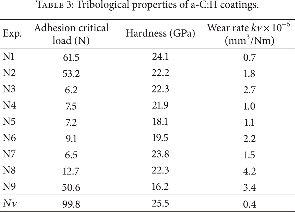
Table 3 shows the critical loads of the nine a-C:H coatings configured in the Taguchi orthogonal array. It is seen that the critical loads vary widely depending on the processing parameters applied. Of the various coatings, N3 has the lowest critical load (6.2 N), while N1 has the highest (61.5 N). It is seen in Figure 1(a) that the periphery of the scratch track on the M2 substrate with the N3 coating has a sawtooth-like breakage pattern. Moreover, the substrate is clearly visible at the base of the track. In addition, it is observed that the coating is largely removed from the substrate at the end of the scratch track as shown in Figure 1(b). In other words, it is inferred that the N3 coating has a highly brittle structure. Coatings N4~N8, also characterized by a low critical load, exhibit a similar breakage pattern, as shown in Figures 1(c) and 1(d) for the N5 and N7 coatings, for example. By contrast, some of the N1 coating remains at the end of the scratch trace, and the periphery is more rounded and smooth (see Figure 1(e)). Figure 2 presents a cross-sectional SEM image of the N1 coating. It is seen that the interfacial region of the coating has a dense and continuous structure. In other words, the results confirm the effectiveness of the ion beam assisted PVD method in producing a-C:H coatings with good bonding properties without an intermediate layer given an appropriate specification of the deposition parameters.
Tribological properties of a-C:H coatings.

Scratch test results for (a) N3 coating, (b) N3 coating at the end of scratch trace, (c) N5 coating, (d) N7 coating, and (e) N1 coating.
Cross-sectional image of N1 coating.
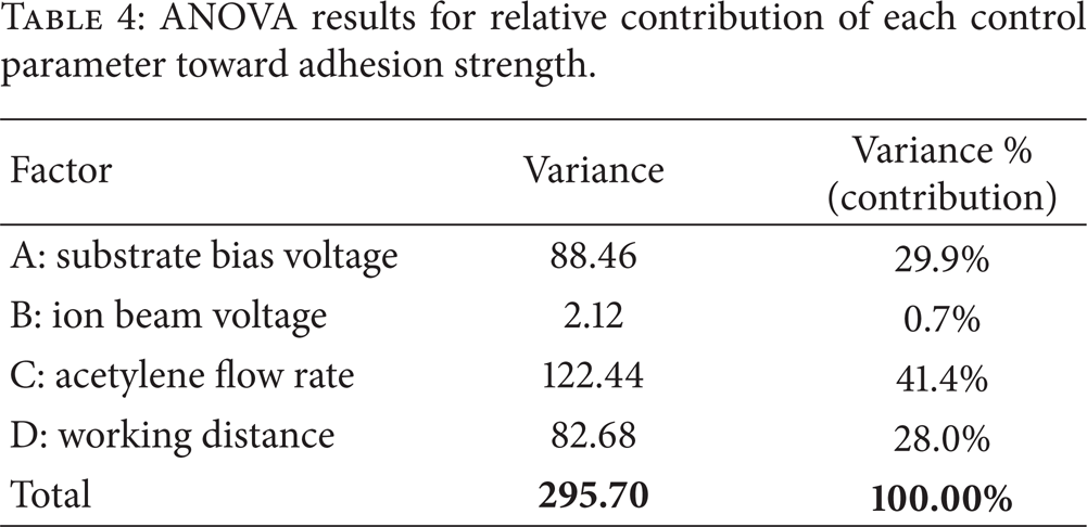
Table 4 shows the ANOVA results for the contribution of each control factor toward the adhesion strength of the a-C:H coatings. Meanwhile, Figure 3 shows the relative effects of each control factor level setting on the adhesion strength of the coatings. It is seen in Table 4 that the coating adhesion is determined principally by the C2H2 flow rate (41.4%). Furthermore, from Figure 3, it is seen that the optimal flow rate has a value of 21 sccm. The substrate bias voltage and working distance have a lesser effect on the adhesion strength (i.e., 29.9% and 28%, resp.). From inspection, the optimal values of the substrate bias voltage and working distance are 0 V and 7 cm, respectively. Finally, it is seen that the critical load is insensitive to changes in the ion beam voltage (0.7%). However, a slight improvement in the adhesion strength is obtained by setting the ion beam voltage as 1.5 kV.
ANOVA results for relative contribution of each control parameter toward adhesion strength.

S/N response graph showing effects of control parameter level settings on adhesion strength.
3.2. Hardness Property
Table 5 presents the ANOVA results for the contribution of each control factor toward the hardness of the a-C:H coatings. The corresponding signal-to-noise response of each of the control factor level settings is shown in Figure 4. The results presented in Table 5 indicate that the coating hardness is determined mainly by the ion beam voltage (39.7%). Moreover, from Figure 4, the optimal value of the ion beam voltage is seen to be 1 kV. The working distance and substrate bias voltage have a lesser effect on the coating hardness, that is, 26% and 24.2%, respectively. In contrast to the adhesion property, the C2H2 flow rate has only a limited effect on the coating hardness (i.e., 10.1%). However, the results presented in Figure 4 suggest an optimal C2H2 flow rate of 12 sccm.
ANOVA results for relative contribution of each control parameter toward hardness.

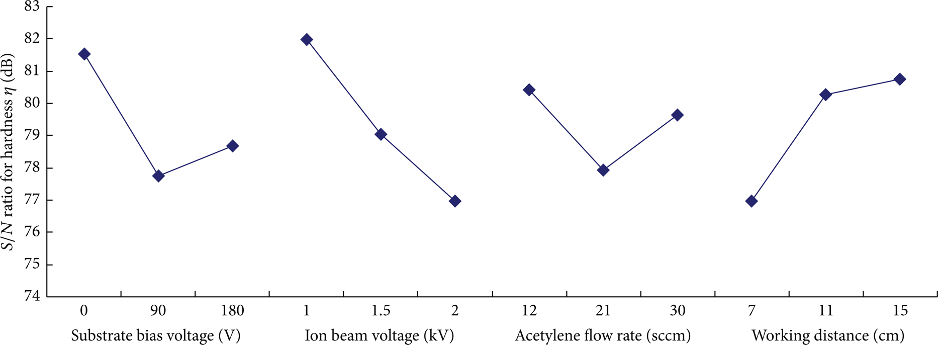
S/N response graph showing effects of control parameter level settings on hardness.
Figure 4 shows that the coating hardness reduces as the ion beam voltage increases. This observation is confirmed by an inspection of Table 3. For example, for coatings N1–N3, the hardness reduces from 24.1 GPa to 22.3 GPa as the ion beam voltage increases from 1 kV to 2 kV. Similarly, for coatings N4–N6, the hardness reduces from 21.9 GPa to 19.5 GPa, while for the N7–N9 coatings the hardness reduces from 23.8 GPa to 16.2 GPa. It is noted that the present results are consistent with those of Kim et al. [21] who found that the sp3 carbon content of DLC coatings reduces with an increasing ion beam voltage and gives rise to a lower hardness as a result.
3.3. Wear Property
The results presented in Table 3 show that the wear rate reduces (i.e., the wear resistance increases) with an increasing adhesion strength and hardness. Thus, the minimum wear rate (N1, kv = 0.7 × 10⁻⁶ mm3/Nm) is observed for the coating with the highest critical load (61.5 N) and the highest hardness (24.1 GPa). Of the nine coatings, N8 has the highest wear rate, that is, 4.2 × 10⁻⁶ mm3/Nm. The SEM image presented in Figure 5 shows that, following the sliding test, the N8 coating is fully removed from the wear trace. Moreover, prominent scratch marks are evident on the underlying M2 substrate. The ANOVA results presented in Table 6 show that the wear resistance of the a-C:H coatings is determined mainly by the ion beam voltage (54.1%) and the substrate bias voltage (31.5%). By contrast, the percentage contributions of the C2H2 flow rate and working distance are just 1.2% and 13.2%, respectively.
ANOVA results for relative contribution of each control parameter toward wear rate.
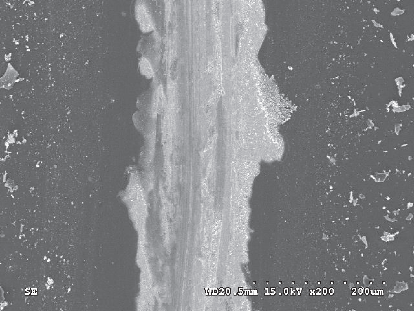
SEM micrograph of wear surface on N8 coating.
Figure 6 presents the signal-to-noise response graph showing the relative effects of each control factor level setting on the wear property of the coatings. The results suggest that the wear resistance of the a-C:H coatings can be optimized by setting the substrate bias voltage as 90 V, the ion beam voltage as 1 kV, the acetylene flow rate as 30 sccm, and the working distance as 7 cm.

S/N response graph showing effects of control parameter level settings on wear rate.
3.4. Confirmation Experiment
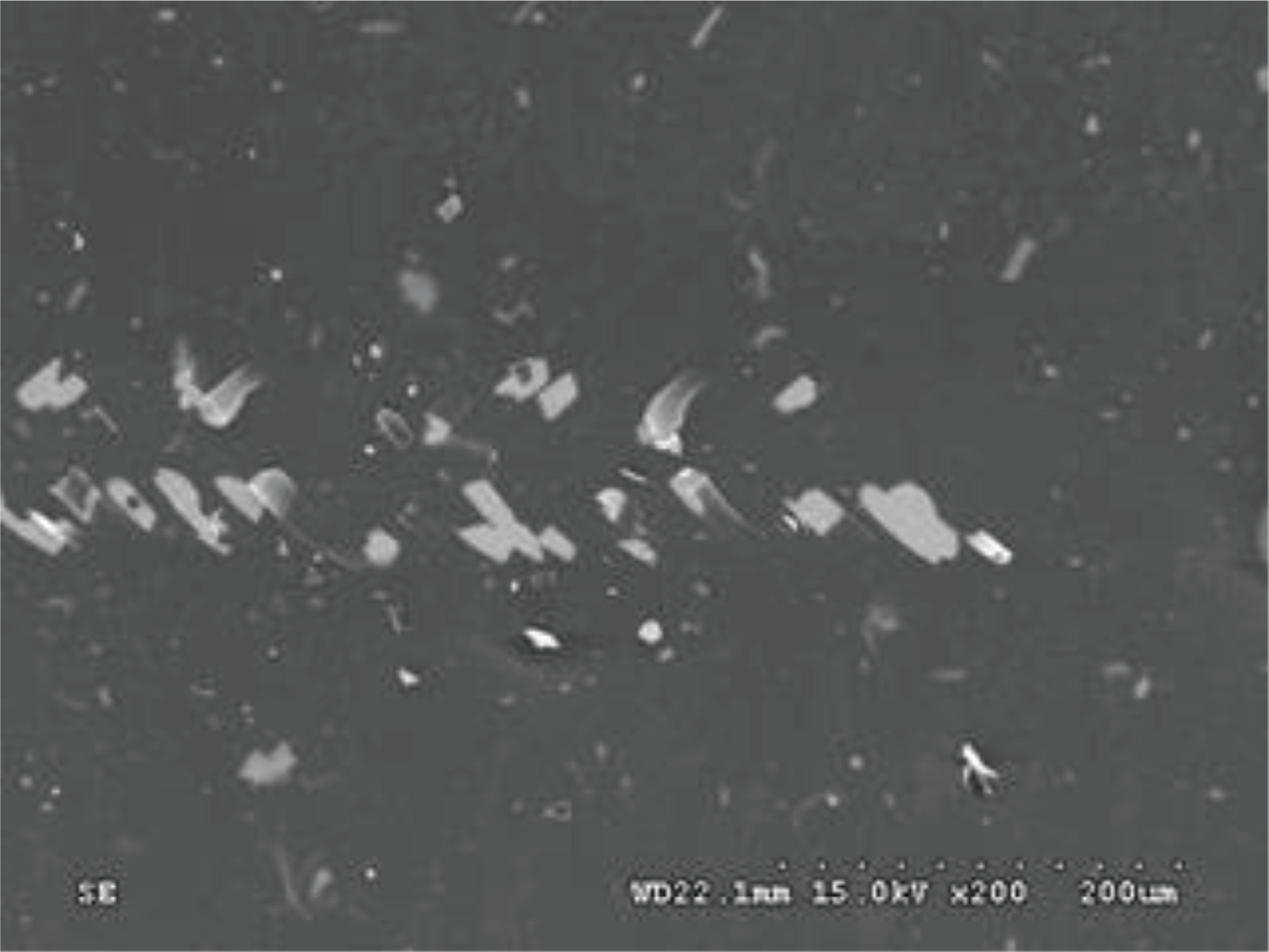
In general, the wear resistance of a coating is one of the most important factors in determining its use in different fields. However, the adhesion strength is also an important concern. Table 4 shows that the contribution of the C2H2 flow rate to the adhesion strength of the present coatings is equal to 41.4%. By contrast, Table 6 shows that the contribution of the C2H2 flow rate to the wear resistance is just 1.2%. Thus, in performing the confirmation experiment, the level settings for the substrate bias voltage, ion beam voltage, and working distance were assigned the values which maximize the wear resistance, while the level setting of the C2H2 flow rate was assigned the value which maximizes the adhesion strength. In other words, the confirmation experiment was performed using control factor level settings of A2, B1, C2, and D1, respectively. As shown in the lower row of Table 3, the optimized coating was found to have a critical load of 99.8 N, a hardness of 25.5 GPa, and a wear rate of 0.4 × 10⁻⁶ mm3/Nm. The SEM image presented in Figure 7 shows that the optimized coating remains largely intact following the scratch test. Moreover, the wear surface has a very smooth and uniform characteristic, as shown in Figure 8. An inspection of Table 3 shows that the optimized coating reduces the wear rate by around 42% compared to that of the original coating with the best wear rate performance (i.e., N1). Moreover, it is seen that the optimized coating also has a higher critical load and hardness than any of the original coatings. Thus, the success of the Taguchi design method in enhancing the tribological properties of the a-C:H coatings is confirmed.
Scratch test results for optimized a-C:H coating.

SEM micrograph of wear surface on optimized a-C:H coating.
4. Conclusion
This study has utilized the Taguchi robust design method to optimize the adhesion, hardness, and wear properties of a-C:H coatings deposited on AISI M2 steel substrates using the ion beam assisted physical vapor deposition (PVD) method. The experimental results support the following major conclusions.
a-C:H coatings with a good adhesion performance can be deposited directly on AISI M2 substrates without an intermediate layer given a suitable specification of the deposition parameters.
The hardness of the deposited a-C:H coatings is determined mainly by the ion beam voltage. As the ion beam voltage increases, the hardness reduces due to a reduction in the sp3 content of the coating.
The Taguchi analysis results show that, for the current a-C:H coatings, the optimal processing conditions are based on the best wear resistance and adhesion strength of the coatings as follows: a substrate bias voltage of 90 V, a ion beam voltage of 1 kV, an acetylene flow rate of 21 sccm, and a working distance of 7 cm, the optimal processing conditions.
The optimal processing parameters yield an effective improvement in the adhesion, hardness, and wear properties of the a-C:H coatings. Specifically, the critical load is increased from 61.5 N to 99.8 N, the hardness is increased from 24.1 GPa to 25.5 GPa, and the wear rate is reduced from 0.7 × 10⁻⁶ mm3/Nm to 0.4 × 10⁻⁶ mm3/Nm. It is noted that the present results for the critical load and hardness are higher than those obtained in a previous study for Zr-C:H:N coatings, that is, 75 N and 21.6 GPa, respectively [14]. Overall, the results suggest that the optimized a-C:H coating has significant potential for various applications in the tribological, cutting, and molding fields.
Conflict of Interests
The authors declare that there is no conflict of interests regarding the publication of this paper.
Footnotes
Acknowledgments
The authors gratefully acknowledge the financial support provided to this study by the National Science Council of Taiwan under Contract no. NSC100-2221-E270-008. The authors would also like to thank Mr. Ting-Ping Cho and Mr. Chao-Hsien Lin of the Micro/Meso Mechanical Manufacturing R&D Department of the Metal Industries Research and Development Center, Taiwan, for their valuable assistance throughout the course of this study.