
Abstract
We have reviewed the deposition of titanium nitride (TiN) thin films on stainless steel substrates by a DC magnetron sputtering method and annealing at different annealing temperatures of 500, 600, and 700°C for 120 min in nitrogen/argon atmospheres. Effects of annealing temperatures on the structural and the optical properties of TiN films were investigated using X-ray diffraction (XRD), atomic force microscope (AFM), field emission scanning electron microscopy (FESEM), and UV-VIS spectrophotometer. Our experimental studies reveal that the annealing temperature appreciably affected the structures, crystallite sizes, and reflection of the films. By increasing the annealing temperature to 700°C crystallinity and reflection of the film increase. These results suggest that annealed TiN films can be good candidate for tokamak first wall due to their structural and optical properties.
1. Introduction
Titanium nitride (TiN) thin films were used for diffusion barriers, gate electrodes in field-effect transistors (FET), contact layers in solar cells, and replacement of polycrystalline Si in large-scale integrated circuits due to their excellent hardness, wear resistance, and metallurgical and chemical stability [1–4]. In nuclear fusion power research, the plasma-facing material is any material used to construct the plasma-facing components, those components exposed to the plasma within which nuclear fusion occurs, and particularly the material used for the lining or first wall of the reactor vessel [5–9]. Selection of the plasma facing mirrors material and research on the behavior of these mirrors under plasma irradiation are currently underway all over the world [10, 11]. Understanding of the plasma-wall interactions provides the basis for developing new materials or choosing among existing ones. Compatibility between the fusion plasma and the surrounding materials is one of the main challenges for the construction of a fusion reactor. For the most exposed areas in a tokamak, the aim is to develop materials that are heat resistant, thermally conductive, and resistant to physical and chemical erosion and show low fuel retention. The sputtering performance of plasma facing components (PFCs) surface materials is critical to future fusion devices. The critical issues are (1) net erosion rates and lifetime, (2) tritium code position in redeposited materials, and (3) core plasma contamination. As recently reviewed in [12], erosion/redeposition codes have been extensively used to assess PFC sputtering performance, with most of the focus, however, being on b or limiter surfaces. There has been much less work done on wall erosion and on mixed material surfaces. Plasma energy containment in tokamak fusion devices is considerably dependent on impurity radiation from the plasma. The amount of impurity radiation is almost proportional to Z3, where Z is the atomic number of impurity ions. Low Z materials (such as graphite), high melting point and high thermal conductivity (such as carbon and tungsten), low nuclear activation, and low propensity to absorb tritium (favouring tungsten most of all, steel and beryllium less, and all but ruling out carbon-based material) are therefore considered to be candidate materials for the limiter and the wall which are the source of plasma impurities. Because of the high radiation of neutron and gamma rays in tokamak, all of the optical components that are close to plasma center must be metallic mirrors because, in contrast to the characteristics of the refractive optical components, the optical properties of metal mirrors are not significantly affected by any of these radiations [13]. It is well known that the TiN coated on S.S.316L has a good capability of maintaining a smooth surface for a long time due to its unique optical and mechanical properties [14, 15]. Currently there is a great interest in designing and engineering thin films with morphologies tailored to specific requirements for various application fields. The connection between the surface morphology of the films and functionality is especially important for optical applications, as surface microstructure generates scattering and stray light in optical components [6–8]. Physical vapor deposition (PVD) techniques such as direct-current (DC) magnetron sputtering, ion plating, and plasma-based ion implantation are employed to deposit TiN thin films [16–18]. Process conditions in PVD techniques affect microstructural features and different physical properties of TiN thin films. In this study, TiN thin films are prepared by DC magnetron sputtering method on stainless steel 316L (S.S.316L) substrate. The effect of annealing temperature on the microstructure, preferred layers orientation, surface morphology, and optical properties of the TiN thin films is investigated.
2. Experimental Method
Titanium nitride thin films were deposited with a DC planer magnetron sputtering system, which is shown in Figure 1(a), using a circular 50 mm diameter and 2 mm thick Ti target of 99.998% purity. The target-to-substrate distance was at 3 cm. A continually variable DC power supply of 700 V and 15 mA was used as power source for sputtering. The substrates were 10 × 10 mm2 stainless steel 316L (S.S.316L) and were ultrasonically cleaned in acetone and ethanol. The substrate temperature was 300°C. The base pressure was lower than 2 × 10⁻⁵ Torr. Pure argon gas and nitrogen gas were used as sputter and reactive gases, respectively. A reactive gas mixture of 95% argon and 5% nitrogen in volume was used at 2 × 10⁻² Torr. With Ar+ bombardment on titanium target and reaction of titanium with nitrogen in plasma the titanium nitride was deposited on stainless steel 316L (S.S.316L) substrate fixed on the sample holder. The growth time for all three samples was 120 min. The deposited samples were furnace-annealed under nitrogen/argon for 120 min at temperatures of 500, 600, and 700°C (Figure 1(b) and Table 1). The crystal structures of the deposited films were evaluated by X-ray diffraction (XRD) with Cu Kα radiation (1.5405 Å); the surface roughness of the films was studied with an atomic force microscope (AFM) and optical property was studied with UV-VIS spectrophotometer.
The RMS roughness for different annealing temperatures.

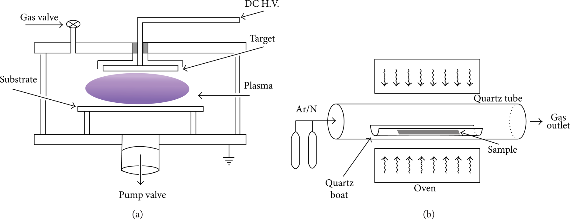
Schematic view of (a) sputtering system and (b) oven used in this experiment.
3. Results and Discussion
XRD patterns of all TiN on S.S. thin film samples (as-deposited and annealed) prepared in this work are shown in Figure 2. The XRD pattern of the deposited film in addition to the substrate peak shows a weak peak at 35.33° that can be related to the (111) crystallographic orientations of TiN with a face-centered cubic (FCC) structure (with reference to JCPDS card number 02-1159; 2θ = 35.317°). It is known that FCC structure of TiN may form when nitrogen atoms occupy all the octahedral sites of titanium with hexagonal close-packed (HCP) or body centered cubic (BCC) structures. This transformation in titanium structure from HCP and BCC to FCC structure occurs due to accommodation of nitrogen atoms with small size in the interstitial sites of Ti with larger size. The absence of a titanium peak in the XRD pattern demonstrates the absence of Ti atoms in the structure of the films and completes nitride formation process. The competition between the surface energy, the strain energy, and the stopping energy of different lattice planes of a film affects the preferred orientation and lowest total energy of the film [17, 19]. In case of TiN film, the direction of lowest energy is
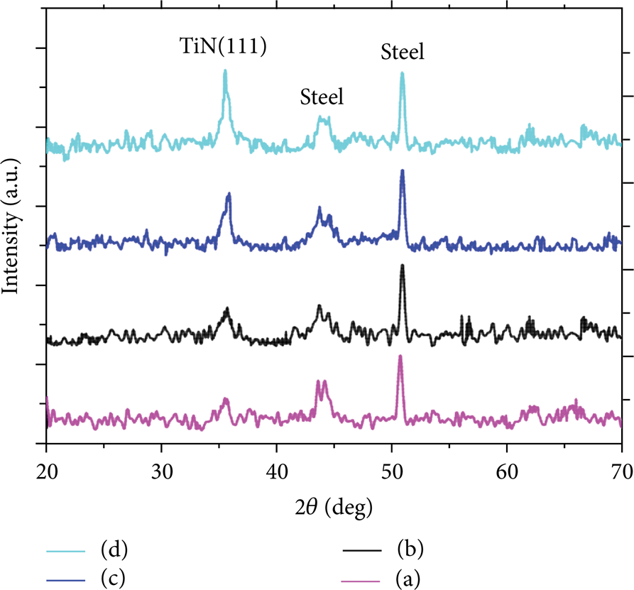
X-ray diffraction patterns of prepared TiN thin films (a) as-deposited and annealed at different annealing temperatures (b) 500° C, (c) 600° C, and (d) 700° C.

FESEM images of TiN thin films as-deposited and annealed at different annealing temperatures.
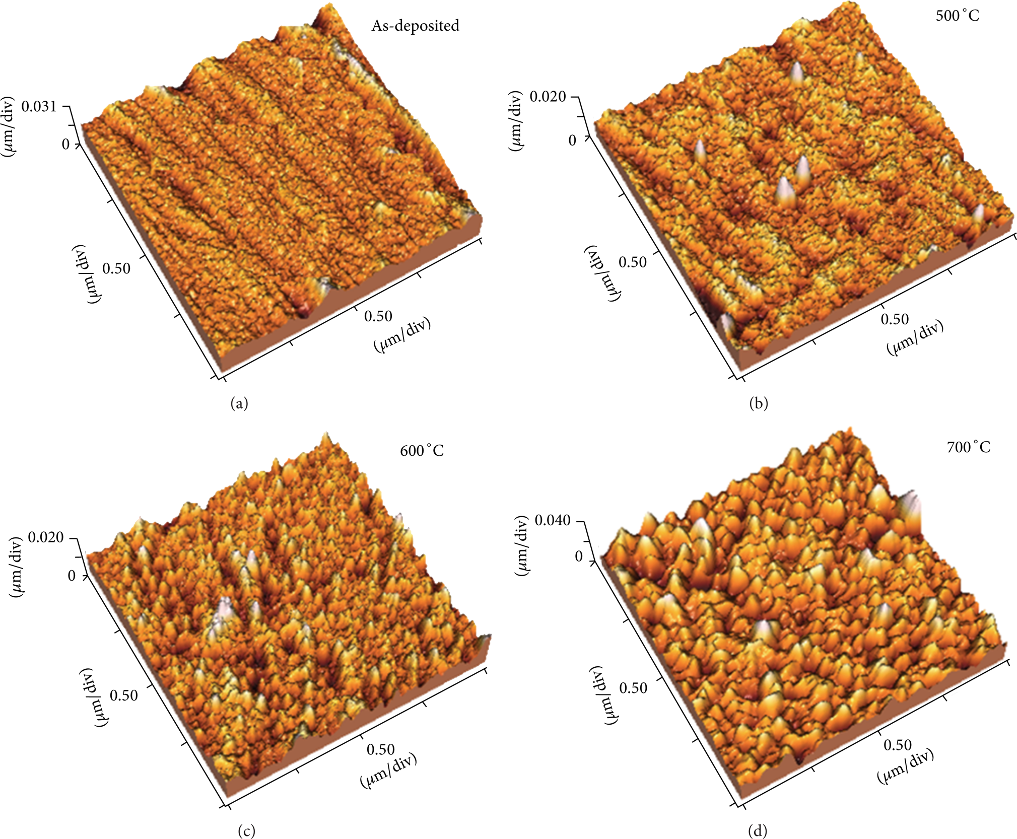
AFM images of TiN films with different annealing temperature, as-deposited and annealed at different annealing temperatures.

Reflection spectra of prepared TiN thin films (a) as-deposited and annealed at different annealing temperatures (b) 500° C, (c) 600° C, and (d) 700° C.
4. Conclusions
TiN thin films were prepared by DC magnetron sputtering method, and it was thermally annealed at different temperatures. The structural and optical properties of the TiN thin films were characterized using XRD, AFM, and UV-Vis spectrophotometer. The grain size of the films increases with the increase of annealing temperatures. The increase in the annealing temperatures causes the atoms to receive a more diffuse activation energy and then to migrate into the energetically favorable site in the crystal lattice. The XRD diffractogram revealed that the thermal annealed film at 700° C possesses good crystalline face-centered cubic (FCC) structure, with a preferred plane orientation along (111). The diffraction peaks of the film become more intense when the annealing temperature increases, which in turn leads to increase in the grain size as well as the enhancement of crystallinity. The TiN films show an increase of reflection with the increase of annealing temperature.
These results show that TiN on stainless steel substrates has a good capability for tokamak first wall due to its fine grain structure, high reflectivity, and hardness property.
Conflict of Interests
The authors declare that there is no conflict of interests regarding the publication of this paper.