
Abstract
An effective simulation approach is introduced in this paper to study the thermal fluid-structure interaction (thermal FSI) on the effect of pin-through-hole (PTH) diameter on the wave soldering zone. A 3D single PTH connector and a printed circuit board model were constructed to investigate the capillary flow behavior when passing through molten solder (63SnPb37). In the analysis, the fluid solver FLUENT was used to solve and track the molten solder advancement using the volume of fluid technique. The structural solver ABAQUS was used to examine the von Mises stress and displacement of the PTH connector in the wave soldering process. Both solvers were coupled by MpCCI software. The effects of six different diameter ratios (0.1 < d/D < 0.97) were studied through a simulation modeling. The use of ratio d/D = 0.2 yielded a balanced filling profile and low thermal stress. Results revealed that filling level, temperature, and displacement exhibited polynomial behavior to d/D. Stress of pin varied quadratically with the d/D. The predicted molten solder profile was validated by experimental results. The simulation results are expected to provide better visualization and understanding of the wave soldering process by considering the aspects of thermal FSI.
1. Introduction
Simulation analysis plays a significant role in engineering applications, such as in the modeling of biomechanical devices, aircraft structures, automotive components, and microelectronic devices. The rapid development of simulation modeling facilitates predictions on real situations. Therefore, it is beneficial in small-scale and complex geometry. Moreover, it can minimize the cost of long-term research activity. Simulation modeling has several applications in electronic packaging, such as integrated circuit (IC) encapsulation [1], fluid-structure interaction (FSI) in molded underfill [2], wire sweep analysis [3], thermal coupling method on ball grid array package reflow soldering [4], and flexible printed circuit board (PCB) [5].
Multiphysics simulation modeling is important to model and solve any phenomenon that involves fluid-thermal and fluid-structural interactions. The fluid and structure are usually treated as a single dynamic element in the direct coupling scheme. Therefore, the governing equations in each model are integrated simultaneously in the domain [6]. Researchers had utilized different boundary formulation methods, for example, coordinate transformation [7], moving reference frames [8], embedded-boundary formulations [9, 10], and nonboundary conforming formulations [11]. Typically, to solve the multiphysics problem, a coupled simulation is required that enables the simultaneous analysis of either fluid-structure or thermal-structure process. A complex flow field may involve heat and mass transfer combined with the stress, deformation, and pressure distribution of a solid structure [12]. Thermal FSI analysis may also be utilized to solve high nonlinear problems [6]. Therefore, a huge amount of computing time is needed for the simulation analysis.
Several studies have been carried out using the simulation coupling approach to solve the multiphysics problem in electronic packaging. Wire sweep and paddle shift phenomenon in encapsulation were solved using the integration of fluid solver FIDAP [13, 14], C-MOLD [15], MOLDEX3D [16] with ABAQUS, and ANSYS (structural solver). However, the simulations of both fluid and structural were analyzed separately. Su et al. [14] suggested ABAQUS and ANSYS software for excellent structural analysis. The two-way coupling simulation method was employed by Yang et al. [17] to predict wire sweep in encapsulation. In recent years, real-time FSI and thermal-coupling methods have been employed to model FSI and thermal-structural phenomena in wire deformation [18], molded underfill [19], reflow soldering [20], and mechanical aspects of flexible PCB [21]. Researchers used the MpCCI coupling method to integrate FLUENT and ABAQUS. The simulations were carried out simultaneously, and real-time data transfer was handled by MpCCI software. The predictions of this coupling method yielded reliable simulation results.
With the high demand in microelectronics industry in recent years, the simulation of a coupled FSI becomes an important tool for clear visualization. The key factor to satisfy the geometrical compatibility at the interface between fluid and structure is FSI analysis. In the PCB assembly, thermal FSI is involved in wave soldering. The pin-through-hole (PTH) components experience high molten solder temperature while passing through the wave solder pot. High temperature imposed on the pin structure may induce thermal stress and displacement, which may influence the molten solder filling in the PCB hole. Moreover, the small PCB hole is limited in specific visualization tools. Therefore, simulation-modeling tools are employed to model the wave soldering process. The physicochemical property of the wave soldering process is revealed in the simulation results.
This study focuses on thermal FSI analysis in the wave soldering process. The main issue in wave soldering is the reliability and quality of solder joint on the PCB. Examples of solder joint defects are cracks, void formation, and unfilled PCB hole (<50%). To address these problems, obtaining a complete understanding of wave soldering is significant to engineers. The visualization of a molten solder capillary flowing through PCB is difficult because of the small size of PTH. The intermediate space between PTH and PCB significantly affects capillary flow. Moreover, the study on the wave soldering process through thermal FSI remains limited in the literature. Therefore, this topic is considered in the present study to examine the effects of PTH diameter on the wave soldering process using the thermal FSI simulation approach. The contribution of this study is to enhance the understanding on the geometrical dimension with detailed visualization of capillary flow in the wave soldering process. The solder profile through PCB is validated by the experimental result, demonstrating the excellent capability of the proposed method in solving thermal FSI in wave soldering.
2. Mathematical Model
The coupling software, Mesh-based parallel code coupling interface (MpCCI 4.1) software [24], was used for bidirectional coupling for CFD and structural analyses [4]. In thermal FSI modeling, finite volume-based solver (FLUENT) was used to simulate the fluid behavior. Finite element-based solver (ABAQUS) was utilized for solid analysis. The fluid and structural solvers were run simultaneously. In the simulation, the molten solder was assumed to be incompressible and was expressed by governing equations. A single PTH connector with various diameters was considered in the simulation. In the actual experiment, the PTH connector interacted with the surface of the molten solder fountain. Thus, only this soldering stage was considered in the present study. 3D fluid flow transports were described by conservation of mass, momentum, and energy as follows.
Conservation of mass (Continuity equation):
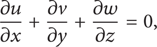
where u, v, and w are velocity in x-, y-, and z-axis, respectively.
The mass conservation equations in x, y, and z directions for incompressible flows are as follows [3]:

where ρ is the density, u is the velocity vector, P is the static pressure, η is viscosity, and g x , g y , and g z are gravity in the x-, y-, and z-axis, respectively.
Energy equation:

At a high temperature, the molten solder has nearly constant viscosity [25]. Therefore, the Newtonian fluid equation is

where τ is the shear stress and
The multiphase volume of fluid (VOF) model with implicit scheme was applied for flow front tracking during wave soldering. The main concept of the VOF scheme is to locate and evolve the allocation of the liquid phase by assigning for each cell in the computational grid a scalar, F, which is the cell's volume fraction occupied by the solder material. As a result, F = 1 in the cell, which contains only the molten solder; the value F = 0 in cells that are void of resin; and 0 < F < 1 at the “interface,” which is referred to as the melt front of the molten solder.
The governing equation of the melt front over time [26] is expressed as

The momentum equation in finite element method (FEM; ABAQUS) was used to solve the structural deformation. The governing equation is [26]
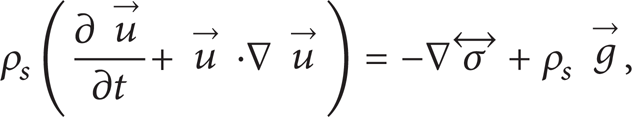
where ρ
s
is the structure density,
3. Sample Preparation and Experimental Setup
A wave soldering experiment using a set of PTH connectors was carried out to validate the predicted simulation results. The circular PTH connector (d/D = 0.2) was inserted into the PCB prior to the wave soldering process. The solder pot temperature was heated to 250°C to melt the solder material. Next, the PCB with PTH connector was passed through the molten solder. The capillary effect of the PCB hole enabled the molten solder to fill the space. Afterwards, the soldered PTHs were solidified at the cooling zone to form a joint on the PCB. Subsequently, the part of the assembled PTH was cut out from the PCB assembly using a diamond wire saw cutting machine. The assembled PTH connector and PCB were molded in a specimen using the resin cold mounting method. After the resin solidified, the specimen was cross-sectioned and then polished in the desired surface area for further analysis using an optical microscope. Figures 1 and 2 illustrate the optical microscope and the specimen for the experimental analysis.
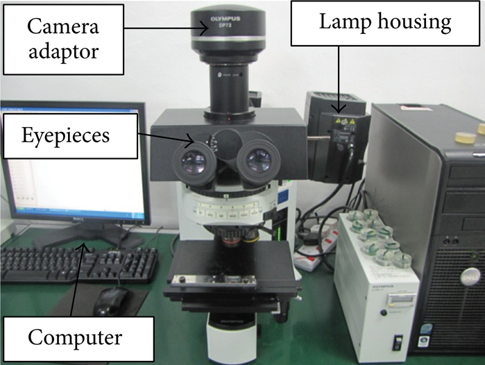
Optical microscope.

Specimen of PTH connector after resin cold mounting.
4. Computational Models
In this study, two different solvers were used, FLUENT 6.3.26 for fluid flow analysis and ABAQUS 6.11 for structural analysis. The fundamental concept of thermal FSI modeling is the coupling of the finite volume method and FEM-based software in monitoring the thermal fluid and structural analyses through an MpCCI. MpCCI facilitates the real-time coupling of these two solvers. During thermal FSI simulation, the MpCCI interpolates the distribution of fluid-induced thermal on the structural mesh. MpCCI software also enables the data exchange between meshes of two simulation codes (i.e., FLUENT and ABAQUS) in the coupling region. It keeps track of the distribution of the domains, enables the exchange of mesh data, and updates the FLUENT meshes. Thus, stress and deformation of the structure were calculated simultaneously. In the current analysis, the pin component structure is defined as the coupled region. The capillary flow front in the PCB hole was solved using FLUENT. ABAQUS was used to calculate the von Mises stress and the displacement of the pin component during the wave soldering process.
4.1. CFD Model
Figure 3 shows a 3D geometrical model of the PCB and PTH created for a single pin. The edge, surface, and volume mesh were developed using CFD preprocessing software (GAMBIT) and exported to FLUENT for analysis. The grid dependency test was carried out to optimize the mesh size. The fine mesh was generated around the PCB and PTH regions, with 272360 tetrahedral elements for the model as illustrated in Figure 3. Different time step sizes were tested to improve the accuracy of the results. Time step size of 0.0001 s was found to be the optimum one for the computational time. Figure 3 also illustrates the boundary conditions of the 3D model. The surface of the PCB, PTH, and solder pot is defined as wall boundaries under the no-slip condition [26]. A pressure boundary was assigned at the inlet and outlet. An interior was placed on the bottom surface of the PCB assembly, as shown in Figure 3. The boundary and initial conditions for the simulations are as follows:
on wall:

on melt front:

where ΔP is the pressure difference between the inside and outside of the curved liquid surface.
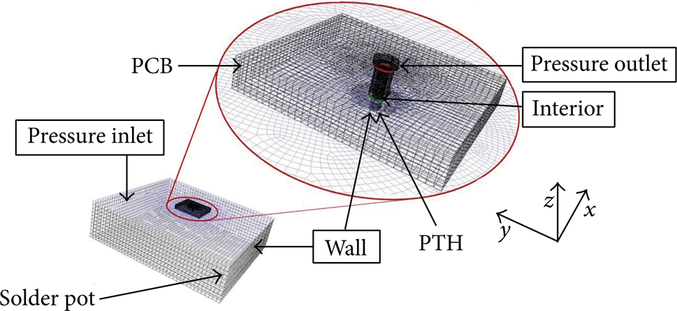
Meshed model and boundary conditions.
In this study, the filling of the PCB hole was assumed to be nonisothermal during the simulation. The solder pot temperature was set to 250°C. The liquidus temperature of the molten solder was also 250°C. Air and molten solder are defined as two distinct phases in FLUENT. Laminar viscous model was used to model air and molten solder phases during wave soldering. The VOF model with implicit formulation was enabled to solve a set of momentum equations. This equation was explained by the volume fraction of the fluid in the computational cell [27]. The SIMPLE algorithm was applied for the pressure-velocity coupling, and the second-order upwind scheme was used for the discretization of each equation to improve reliability [20]. In the real wave soldering process, the fountain of molten solder form is stable. Therefore, the effect of the turbulence flow by propeller was neglected in the current simulation. Six different PTH diameter profiles were considered in the current study. The PTH pin height is 3.50 mm. The diameter ratio of pin relative to the PCB hole (0.1 < d/D < 0.95) is summarized in Table 1. The PCB, PTH component, and solder pot were cross-sectioned by Section 1 (Figure 4) to visualize the molten solder profile using various PTH diameters. The predicted results were compared with the solder profile of ratio d/D = 0.2 as observed in the experiment.
Diameter profile (bottom view).

Cross-sectional view of PCB, PTH component, and solder pot at Section 1.
4.2. Structural Model
Figure 5 shows the PTH pin coupled region for structural analysis. A 3D meshed model was developed using the hexahedral sweep method in ABAQUS 6.11. The PTH mesh size was optimized for better accuracy during computational time. The structural solver simulated the temperature distribution, which corresponds to the molten solder temperature in the PCB hole. A coupled temperature displacement was considered for thermal and stress analyses [24]. The structures of the coupled regions are defined as deformable in ABAQUS. The PTH was assumed to be a copper pin. In the experiment, the structure of the PTH head was properly fixed during the wave soldering process so the fixed boundary condition was set on top of the PTH pin. The thermal and material properties used in the structural analysis are summarized in Tables 2 and 3, respectively. Some basic assumptions were considered in the FEM simulation. The uniform wetting profile was assumed in PCB and PTH. Therefore, the effect of flux was not considered in the study. The temperature effects on the pin stress and displacement were considered in the thermal FSI modeling.
Material properties used for the PTH connector.

Thermal properties of PTH connector.


Structural meshed model.
5. Grid Independence Test
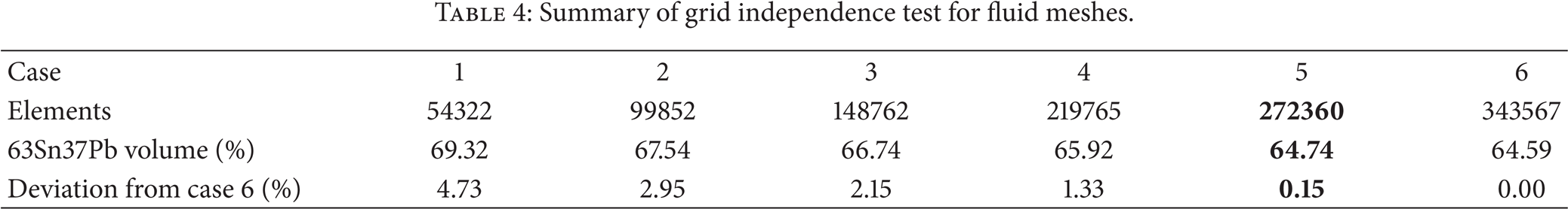
In this section, the effects of meshes are examined on the fluid domain and solid structure. The optimum mesh size prior to fluid and structural analysis was selected to obtain better accuracy and minimize the discretization error. The fluid and solid meshes are defined as independent when the volume integral (phase) of the molten solder of the PTH and PCB does not exceed ± 0.5% between successive meshes. Table 4 presents the summary of the grid independence test. Six cases (i.e., Cases 1 to 6) are referred to as 5.432 × 10⁴, 9.985 × 10⁴, 14.876 × 10⁴, 21.977 × 10⁴, 27.236 × 10⁴, and 34.357 × 10⁴ elements. The volume of molten solder at t = 1.0 s was evaluated for each case. The deviations in volume fraction of Cases 1 to 5 were calculated by referring to Case 6, which has the greatest number of elements. A better percentage nominal deviation (0.15%) was found between Cases 5 and 6. The filling volume showed a linear relationship to the filling time. Figure 6 clearly illustrates the comparison of volume (in percent) sizes versus filling time of various meshes. Thus, Case 5 was chosen as the optimum mesh size in terms of moderate computing time.
Summary of grid independence test for fluid meshes.
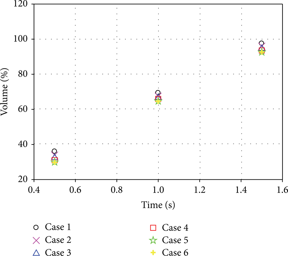
Volume of molten solder versus time for various mesh sizes in fluid analysis.
The grid independence test of the structural analysis is summarized in Table 5. Case 1 has the coarsest meshes; conversely, Case 5 has the finest meshing element. The volume deviations of the molten solder at t = 1.0 s were evaluated. Insignificant variances when increasing the number of elements in structural analysis were found. Cases 4 and 5 demonstrate better performance than other cases, with lower deviation (0.10%) between both cases. Figure 7 shows the comparison of molten solder volume versus time for various mesh sizes. Case 5 was chosen as the optimum mesh size for structural analysis.
Summary of grid independence test of structural analysis.


Volume of molten solder versus time for various mesh sizes of structural analysis.
6. Results and Discussion
6.1. Experimental Validation at 50% Filling Time
Prior to further simulation analysis, the predicted simulation result (d/D = 0.2) was used to substantiate the proposed MpCCI coupling method in the filling of molten solder. The predicted result was compared with the actual experimental result. The profile of molten solder in the experiment was difficult to observe because of the small and nontransparent PCB hole. Therefore, only the solidified solder profile was compared in this study. Figure 8 shows the comparison of simulation and experimental solder profiles at 50% filling time. Both solder profiles have identical shapes and similar filling levels. The predicted solder volume was compared with the experimental result (Figure 9). The discrepancy of both solder volumes was only 7.13%. Therefore, the result indicates the excellent capability of MpCCI software in solving molten solder filling problem by considering thermal FSI.

Validation of predicted and experimental results.

Volume of molten solder at 50% filling time.
6.2. Overview of the Thermal Structure Analysis (d/D = 0.2)
The PTH pin displaces or expands when it experiences high soldering temperature. In the current simulation, the MpCCI thermal coupling method transfers heat and temperature of the molten solder to ABAQUS for structural displacement, stress, and temperature. Overheating of the component may cause failure, such as resistor and capacitor malfunction. Extreme displacement and stress concentration on the pin may induce an initial defect for subsequent process. Thus, simulation modeling can provide a better understanding of the physic chemical property of wave soldering. Figure 10 illustrates the simulation results of FLUENT and ABAQUS. A FLUENT solver models the molten solder behavior and tracks the flow advancement. Displacement and stress imposed on the PTH pin were solved by ABAQUS. In the wave-soldering simulation, molten solder filled the PCB hole driven by the capillary effect. The inserted pin in the PCB hole was subjected to the molten solder temperature, as shown in Figure 10. The displacement profile of the PTH pin corresponded to the filling level of the molten solder in PCB hole. These temperature and thermal structure effects are difficult to measure in an actual experiment. Therefore, the proposed simulation method can be used to overcome these difficulties.

Thermal structure profile at t = 1.0 s.
6.3. Filling Profile at t = 1.0 s
The molten solder profile was evaluated for different PTH pin diameters during wave soldering at 1 s filling time. Figure 11 shows the effect of the PTH pin diameter on the molten solder profile. The intermediate space between the pin and the PCB hole surface became narrow when the pin diameter increased. Figure 11 shows the molten solder profile of d/D = 0.1 (smaller pin diameter) to have different filling profiles. Molten solder tends to flow easily in free space. Thus, the filling of the molten solder in case d/D = 0.1 was concentrated in the middle region of space. However, the solder profile of d/D = 0.2 and 0.4 had a similar shape around the PCB wall. The molten solder level on the PCB wall was higher than that in the PTH pin, forming a racetrack effect in the filling process. This situation can be attributed to the widening PCB hole surface compared with that of the PTH pin. The maximum and minimum molten solder levels are plotted in Figure 12. The filling level showed polynomial behavior with the increment of d/D. The increase in the d/D ratio resulted in faster filling because of the narrow intermediate space between the pin and the PCB hole surface. A narrow intermediate space may induce a weak solder joint because of the insufficiency of the solder material to attach the pin to the PCB. Therefore, a fundamental understanding of wave soldering is important to engineers in the PCB assembly industry.

Effect of PTH diameters to the molten solder advancement (front view).

Maximum and minimum filling levels (percentage) at t = 1.0 s.
6.4. Pressure Profile of the PCB Hole
As mentioned in Section 6.2, molten solder advancement is driven by the capillary action of the PCB hole. The capillary force results from the pressure difference between the inside and outside of the curved molten solder surface, enabling it to propagate in the PCB hole. This situation was evidently observed in the pressure profile of each case. Figure 13 shows the pressure contour of the PCB hole at 100% filling time. The pressure drop varied in every case. In this figure, the pressure in the solder pot is atmosphere pressure. During the filling process, the molten solder pressure dropped from the bottom PCB until the entire hole was filled. The pressure contour in Figure 13 distributes symmetrically because of the symmetric intermediate space between the pin and the PCB hole surface. The shape of the pressure contour matched with the molten solder profile, as presented in Figure 11. Therefore, the molten solder advancement is the result of the pressure drop in the capillary flow. The pressure distributions on the PCB surface were also evaluated. The molten solder pressure was dropped from the 0 mm position to the 2.4 mm position, as shown in Figure 14. Pressure in PCB for d/D = 0.1, 0.2, 0.4, and 0.6 had a similar trend, with only small variations in the 0 mm to 0.5 mm position. However, the increase in d/D ratio to 0.8 and 0.95 (with small intermediate space) resulted in different trends caused perhaps by the decrease in filling space. This phenomenon was also observed in the gap height effect of the underfill process [28]. Conversely, a decrease in gap height causes the increase in pressure drop.
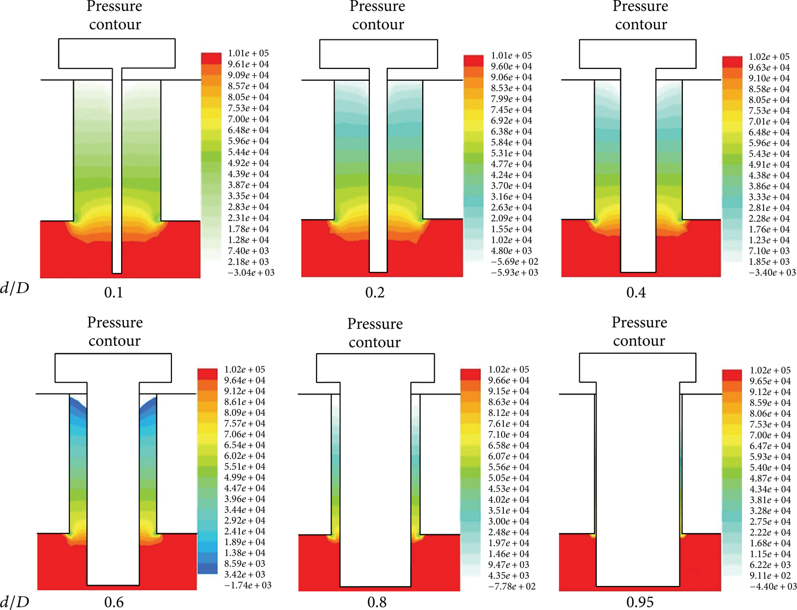
Pressure distribution in PCB hole at 100% filling time.

Pressure distributions within PCB.
6.5. Temperature Distribution on the Pin at 0.37 s < t < 1.58 s (d/D = 0.2)
The proposed thermal FSI analysis predicts the temperature distribution on the pin during wave soldering. Temperature distribution and flow front advancement at various filling time stages for d/D = 0.2 are shown in Figure 15. Figure 16 shows the temperature distribution on pin. Based on the results, the pin experienced heat from the filling of the molten solder. The temperature distribution of the pin corresponded to the molten solder advancement. Overtime, the immersed bottom edge of pin was subjected to increases in temperature, specifically at 0.72 s to 1.58 s. Any improper control of the wave soldering process caused the pin to experience high temperature for a long duration. It may induce high thermal stress and displacement of the pin. Moreover, high temperature may cause the failure of the component if it exceeds the allowable component temperature. In this study, the temperature of various pin diameters was estimated along the position of 0 mm to 3.3 mm, as shown in Figure 15. The temperature showed the polynomial correlation to the d/D, as shown in Figure 17. The highest temperature was found on the smallest pin diameter (d/D = 0.1). The d/D ratio then increased. In this case, the temperature of the pin mainly came from the filled molten solder in the PCB hole. The narrow free space in the PCB hole resulted in the lesser filling of the molten solder [29]. Thus, a low temperature was found for a large pin diameter in this study, as shown in Figure 16.

Temperature profile (contour) on pin at 0.37 s < t < 1.58 s.

Temperature distributions on pin (0.1 < d/D < 0.95).

Temperature variations with diameter ration (d/D).
6.6. PTH Displacement at 50% and 100% Filling Level
The displacement of the PTH pin at 50% and 100% filling levels is examined in this section. Only selected results for d/D = 0.1, 0.2, and 0.95 are presented in Figure 18. In the figure, the displacement contour on the pin is increased from the bottom edge until the top of the pin, as illustrated in the 50% and 100% filling levels. The maximum displacement for each case was concentrated on the bottom edge of pin, which was immersed in molten solder, as mentioned in Section 6.4. This section reveals that pin displacement coincides with the temperature or heat subjected to it. The displacement along the pin at 100% filling was estimated from the simulation results for each case, as presented in Figure 19. The largest pin diameter only displaced 0.0004 mm. Conversely, the smallest pin diameter had the largest displacement (0.0083 mm). The correlation between maximum displacement and d/D ratio is plotted in Figure 20. The maximum pin displacement decreased in polynomial behavior to d/D ratio for both 50% and 100%.
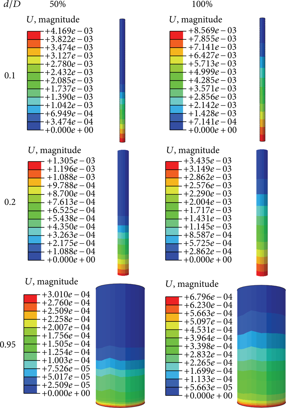
PTH displacement at 50% and 100% filling level.

Displacement along PTH at 100% filling level.

Maximum displacements on PTH at 50% and 100% filling level.
6.7. von Mises Stress at 50% and 100% Filling Level
High thermal stress of the pin may change the initial defect of subsequent manufacturing processes and reduce the solder joint reliability. This section studies the thermal stress of different pin diameters. Figure 21 shows the von Mises stress profile of selected d/D (0.1, 0.2, and 0.95) at 50% and 100% filling levels. The stress imposed on the pin resulted from the thermal effect. The pin experienced high molten solder temperature. In the simulation results, high stress is represented by the red color in each legend. Based on the results (Figure 21), the stress was distributed unevenly on the pin structure, as shown in Figure 22. The stress along the pin was evaluated. This phenomenon can be attributed to the filling process of the molten solder and the conduction of the pin (bottom pin region immersed in the solder pot) under high molten solder temperature. However, stress was concentrated on top of the pin (case d/D = 0.1), which could be caused by displacement, as discussed in Section 6.6. Thus, the stress on the displaced pin varied, as shown in Figure 21 (d/D = 0.1 at 100% filling level). The maximum stress imposed on the pin versus d/D ratio is plotted in Figure 23. The maximum stress was varied quadratically over the d/D ratio. The pin of case d/D = 0.4, 0.6, 0.8 and 0.95 experienced high stress concentration (120 MPa to 150 MPa) at 100% filling level compared with d/D = 0.1 and 0.2 (nearly 70 MPa). High stress should be minimized to prevent initial defect on the assembled component on the PCB. Therefore, physical pin design and process control are crucial in the PCB assembly industry.

von Mises stress at 50% and 100% filling level.

Stress (MPa) along PTH at 100% filling.

Maximum stresses (MPa) on PTH at 50% and 100% filling level.
7. Conclusion
The thermal FSI modeling of the molten solder filling process in PTH was carried out, and the effects of the pin diameter were investigated in this study. The intermediate space between pin ad PCB hole was determined using d/D ratio. In wave soldering, the molten solder was driven by the capillary forces of PTH to fill the space. The increase in pin diameter resulted in a racetrack filling profile and changes in pressure distribution. The temperature profile of the pin clearly indicates that the pin experienced the temperature of molten solder during filling process. The pin of case d/D = 0.1 was displaced by nearly 0.008 mm and caused the stress to be concentrated on the top of the pin. Although the increase in the d/D ratio reduced the displacement of the PTH pin, the pin was subjected to high thermal stress resulting from the conduction effect. High stress imposed on the pin could induce initial defects in subsequent manufacturing processes. Thus, the pin of d/D = 0.2 was the appropriate pin design in terms of filling profile, displacement, and stress. Simulation results revealed that filling level, temperature, and displacement demonstrated polynomial behavior to the diameter ratio. However, stress of pin quadratically correlated with diameter ratio. The simulation results of the solder profile were validated by the experimental results. The excellent capability of the proposed thermal FSI method to handle thermal fluid and structural analyses in wave soldering was demonstrated.
Footnotes
List of Symbols
Conflict of Interests
The authors declare that there is no conflict of interests regarding the publication of this paper.
Acknowledgments
The author gratefully acknowledges the financial support of the Ministry of Higher Education of Malaysia through the My Brain 15 Ph.D. scholarship program and Short Term Research Grant Scheme (SGJP) Universiti Malaysia Kelantan.