
Abstract
Contactless smart cards are being widely employed in electronic passports, monetary payments, access control systems, and so forth, because of their advantages such as convenience and ease of maintenance. In this paper, we present a new side-channel attack method for contactless smart cards. This method exploits the information leakage stemming from electromagnetic disturbances (EMD). We also made a convenient and low-cost EMD reader board that performs side-channel attacks on contactless smart cards. In order to demonstrate that EMDs can become another information-leakage side channel, we have carried out side-channel analysis on a commercial contactless smart card that performs 128-bit ARIA encryptions, and we have been able to successfully find all 16 bytes of the ARIA key from the target device. From our experimental results, we conclude that the proposed EMD analysis yields better results than the conventional power analysis.
1. Introduction
Side-channel attacks exploit information leakage stemming from variations in physical quantities such as timing, power consumption, and electromagnetic (EM) radiation [1–3]. By measuring the variations in processing time, power consumption, and EM radiation during the execution of the target algorithm and correlating these variations with the data being manipulated, the secret key can be obtained from the target device. From among all of the information leakage channels, the information leakage from the electromagnetic radiation is the best for use in side-channel attacks on contactless smart cards because the other information leakage channels are very limited. An EM side-channel analysis exploiting the information leakage stemming from EM radiation has several advantages such as higher signal-to-noise ratio and the ability to bypass the power analysis countermeasures. However, considerable effort is required to measure and analyze the electromagnetic radiation, such as separating the smart card chip radiation from the antenna radiation and filtering the carrier signal [2, 4].
In this paper, we present a new side-channel attack method that exploits the information leakage due to electromagnetic disturbances (EMD) in contactless smart cards. EMDs are an unwanted form of load modulation caused by dynamic load changes. These dynamic load changes are caused by the switching operations of the contactless smart card's internal digital circuits, especially during cryptographic operations [5]. Under ISO 14443, a contactless smart card is also referred to as a Proximity Integrated Coupling Circuit (PICC), whereas the card reader is called a Proximity Coupling Device (PCD). The PICC consumes the energy generated by the PCD in order to gather the energy needed to operate; this energy consumption has the same reactive effect on the PCD as a voltage amplitude modulation. This effect is used to transfer data from the PICC to the PCD by changing the resistive load in the PICC according to the transmitted data bit (0 or 1). This resistive load change in the PICC is also generated by the energy consumption required for processing cryptographic operations or EEPROM programming. This load change (variations in the internal power consumption of the PICC) causes an unwanted form of load modulation, and the EMD becomes another information leakage channel vulnerable to side-channel attacks on contactless smart cards.
Compared to conventional EM radiation,
2. Previous Studies on Contactless Smart Cards
There are three basic types of contactless smart cards: close-coupling cards defined in ISO 10536, proximity-coupling cards defined in ISO 14443, and vicinity-coupling cards defined in ISO 15693. Most commercial contactless smart cards are ISO 14443 compliant. In this study, we focused mainly on a PICC proximity coupling card working at a carrier frequency of 13.56 MHz. Because of several advantages such as convenience and easy maintenance, an increasing number of contactless smart cards are being deployed for various applications such as in electronic passports, for monetary payments, and in access control systems. With this increased use of contactless smart cards, side-channel attacks on contactless smart cards have increased and so these attacks have become an area of intense study; several important studies related to this topic have been published. Carluccio et al. [2] performed an EM attack on a contactless smart card. In order to minimize the adverse influence of the field of RFID readers on the measurements, they separated the chip and antenna radiations and measured the EM radiation by using a near-field magnetic probe, which was placed perpendicular to the chip surface; however, the attack was not successful. Hutter et al. [3] published the first reported results of successful EM attacks on hardware and software AES implementation in RFID tag prototypes. In Hutter's experiment, the target device was not a commercial product but a self-made RFID prototype in which the analog front end, that is, the antenna and the rectifier circuit, was separated from the digital circuit. In commercial products, the analog and digital components are fixed together. The configuration of the target device in Hutter's experiment leads to more EM emissions than in the commercial products and the effect of the field of RFID readers on the measurements could be easily eliminated. The main approach used to perform side-channel attacks in these experiments was indirectly measuring the power consumption via the EM field of the device by using a magnetic near-field probe. However, this was not easy because the carrier signal of the reader was much stronger than the field of the contactless device. In order to minimize the adverse influence of the carrier frequency on the measurements, it is necessary to use complex active and passive analog filters. Therefore, in order to ameliorate these EM measurement setup difficulties, it is necessary to develop more convenient and efficient side-channel analysis methods.
Kasper et al. [4, 7] proposed an analog demodulator specifically designed for filtering the signal measured by an EM probe. In Carluccio and Hutter's works, the EM radiation from the chip surfaces was directly measured using an EM probe. However, the EM radiation from the chip surfaces was much weaker than that of the field signal of the reader. Thus, the attack was not successful. Hutter's approach was successful, but the target device was not a commercial contactless product. To successfully attack contactless cards, Kasper et al. exploited the information leakage that stemmed from amplitude modulation (load modulation) of the 13.56 MHz field of the reader. In [4, 6], the authors assumed that the power consumption of the inductive-coupled smart card leads to very weak amplitude modulation of the field generated by the reader. To extract the weak information leakage from the amplitude modulation signal, the authors used an incoherent demodulation approach. In Kasper's experiment, the EM radiation was measured by an EM probe, while the target was executing an operation. The measured raw signals were processed using an analog demodulator and filter. For this purpose, the authors designed a custom analog circuit for amplification, rectification, and filtering of the raw analog signal. The authors demonstrated the side-channel vulnerability of the Mifare DESFire MF3ICD40 contactless smart card using this approach.
3. EMD Analysis on Contactless Smart Cards
When the proximity cards inductive coupled with readers execute their operations, the variations in the internal power consumption of the proximity cards cause physical changes such as EM radiation from the chip surface and amplitude modulation of a carrier field of the reader inductive coupled with the proximity card. These changes are exploitable in the side-channel analysis.
As described above, in Carluccio and Hutter's experiments, the information leakage from the EM radiations was measured using an EM probe. However, the isolation of very weak EM radiation from a strong carrier field is difficult. Hence, performing the side-channel analysis on proximity smart cards with EM radiation emitted from the chip is challenging. On the other hand, in Kasper's experiment, the authors have studied information leakage caused by amplitude modulation of the carrier field. Their incoherent demodulation approach apparently improved the efficiency of SCA on proximity card but there is no major enhancement in the measurement setup; it is still necessary to use additional complex hardware analogue filter.
Similar to Kasper's study, we have also adopted a demodulation approach but have focused more on the reader demodulation process. The extent of information leakage caused by amplitude modulation could be measured and processed more easily through an ISO 14443 compliant reader demodulation process without any EM probe or additional hardware filter. Proximity cards communicate through intentional load modulation, but variations in the power consumption of the card also create unintentional load modulation [8]. This kind of unintentional load modulation is defined as EMD according to ISO standards [5]. The variations in some cards are so large that some readers detect false card responses. The allowable EMD levels and handling method for the ISO 14443 compliant reader are standardized by ISO [5, 9]. This means that the amplitude modulation that contains the information leakage of proximity cards can also be measured and processed in the reader.
Because the levels of load modulation can be measured through the demodulated signal after IQ demodulation inside the reader [10], the unwanted load modulation EMD can be measured from the demodulated analog signal after the IQ demodulation. This demodulated signal can be also measured easily using the debugging functionality of the commercial contactless smart card reader IC chip. In our experiment, the amplitude load modulation was measured and processed during the demodulation process of the reader. For this purpose, we have designed an EMD measurement board, which is a slightly modified version of the common ISO/IEC 14443 reader. In Kasper's study, the analog demodulated signals were measured to maximize the vertical resolution of the measurements and capture all the relevant information [4, 7]. In our study, we have also measured the amplified demodulated analog signals by configuring the internal register setting of the chip in order to minimize the loss of information. This approach makes it possible to ameliorate the EM measurement setup difficulties as well as to improve the efficiency of SCA on proximity card. In this study, we have used a commercially available smart card, which provides dual communication interfaces (ISO 7816 contact and ISO 14443 contactless) and performs 128-bit ARIA encryption implemented in software without side-channel countermeasures.
4. EMD Measurement Setup
In a side-channel attack on a contactless smart card, the data- and operation-dependent power consumption is generally measured indirectly via the EM field of the target device by using an EM probe [3, 4]. In our approach, instead of measuring the EM field of the target device, the data- and operation-dependent power consumption is measured indirectly via the EMD level of the target device by using an EMD board.
Figure 1 shows the schematic of the EMD measurement setup. The PICC consumes energy generated by the PCD in order to gather the energy required for its operation. In general, the power consumption of the PICC


Schematic of the EMD measurement setup.
The methods for measuring the EMD level of a PICC can be implemented using a spectrum analyzer or a vector signal [10]. In order to demodulate the received RF signal from the card, most commercial readers first perform quadrature demodulation of the 13.56 MHz carrier signal using an IQ demodulator [10]. The IQ demodulator converts an RF input into two intermediate outputs with a 90° phase difference [14]. The demodulated signal is amplified by an amplifier and digitized by the digitizer circuit.
Because the EMD is a kind of load modulation whose levels can be measured through the demodulated signal after IQ demodulation inside a reader, the EMD can also be measured from the demodulated analog signal after IQ demodulation. This demodulated signal can be also measured by using the debugging functionality of commercial contactless smart card reader IC chips. In our experiment, instead of using the complex measurement setups, we designed an EMD reader board, which is a slightly modified version of the common ISO/IEC 14443 reader. The EMD reader board consists of a commercial ISO/IEC 14443 reader IC chip, an RF antenna, and a CPU.
The board is controlled by an ST STM32F103 microcontroller and provides an ISO 14443 compliant RF front end with an NXP MFRC531 reader IC chip and an RF antenna. The board is equipped with a USB interface for communication with a host PC. A USB connector and an external 5.0 V DC power supply provide power for operation of the board. The power supply is physically separated to reduce the power supply noise. Two BNC connectors are placed on the reader board for measuring the EMD signal: an EMD port for the “EMD signal” and a TRG port for the “TRIG signal,” as shown in Figure 1. The microcontroller in the reader board communicates with a host PC and controls the reader IC chip to perform ISO 14443 compliant communication with the card. A trigger-timing signal, which signals the measurement equipment about when to begin acquiring EMD traces, is generated by the microcontroller through the TRG port (Figure 1).
The reader IC chip used in the EMD board basically performs modulation and demodulation for passive contactless communication. The signal received through the antenna of the reader board is forwarded to the reader IC chip through the RF circuit. Quadrature demodulation of the 13.56 MHz carrier signal is performed using the IQ demodulator. The demodulated signal is filtered and amplified within the reader IC chip and digitized in the digitizer circuit.
The reader IC chip is also responsible for measuring the EMD signal of the card. As described above, the EMD can be measured from the demodulated analog signal after IQ demodulation in the reader. Because the reader IC chip used in the EMD reader board has a built-in monitoring functionality, that is, an internal reference voltage and an amplified demodulated analog signal, the EMD signal can be easily measured using the amplified demodulated signal monitoring functionality of the reader IC chip. The amplified demodulated analog signal after the IQ demodulation in the reader is routed to the auxiliary output pin of the reader IC chip using the internal register configuration settings of the chip. The measured EMD signal is output from the reader board through the EMD port placed on the auxiliary output lines of the reader IC chip. The EMD signal, shown in Figure 1, is the demodulated analog signal, which is stored on the host PC after passing through the oscilloscope.
In order to increase the quality of the EM measurements, we have adjusted and optimized the external factor that influences the measurement of the load modulation. From our experiments, it was observed that the load modulation level is inversely proportional to the field strength of the reader.
To change the field strength of the reader, the conductance of the reader antenna was adjusted. In general, the field strength of the reader depends on the conductance of the antenna that can be adjusted using the internal register configuration setting of the chip. By configuring the internal register of the chip, the field strength of the reader was adjusted to a value that was as low as possible yet sufficient to operate the proximity card. This approach was also the most effective and inexpensive for avoiding the adverse influence of the reader field.
Using those approaches, we can measure the EMD during the cryptographic operation of the PICC without additional specific signal processing. Figure 2 shows a picture of the actual experiment configuration. A host PC controls the EMD reader board and the oscilloscope. From the host PC, a smart card application protocol data unit (APDU) and board control commands are transferred into the EMD board through a USB port. The board control commands are used to initialize the connection between the host PC and the EMD board, to set or adjust the timing of trigger signal, and configure the parameters such as the alternative magnetic field strength generated by the reader.
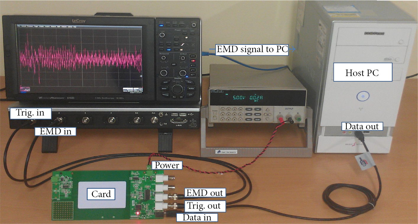
Image showing the experimental configuration.
The EMD reader board is responsible for measuring the EMD signal of the card during its operation. The received signal, including the unwanted load modulation generated by the PICC at its antenna, is forwarded to the reader IC chip of the board through the RF circuit. The received signal is demodulated and amplified within the reader IC chip of the PCD. This amplified demodulated analog signal is routed to the auxiliary output pin of the ISO/IEC 14443 reader IC chip by using the internal register configuration settings of the chip. Then, the measured EMD signal is passed through the oscilloscope and stored on the host PC.
5. Attacks on Dual-Type Smart Cards with the S/W ARIA Implementation
We performed power and EMD side-channel analyses on a commercial dual-type smart card by using the Correlation Power Analysis (CPA) method [15]. CPA exploits the correlation between the power consumption of the target device and its power consumption model. To perform CPA, the attacker measures the power consumption of the target device and then calculates the power estimates of the target from different ciphertexts using a predicted partial key and a power model. Assuming that the power model is valid, the power estimates and the measured power traces are correlated if the partial key prediction is correct. From the key hypothesis, the attackers can find the correction key with the highest correlation coefficient [16]. The target card supports both contact and contactless communication interfaces and performs 128-bit ARIA encryptions in its software.
A power analysis attack was performed as the reference for the EMD analysis attack. The goal of the first EMD analysis attack was to verify that the EMD of the target device indeed leaked side-channel information. The attacks that we discuss in this section used the output of the entire S-box operation in the first ARIA round to reveal all 16 bytes of the secret key. For each attack, 50,000 traces were recorded and the Hamming weight model was employed. Approximately, one day was needed to reveal the keys for performing the EMD analysis using CPA; a half day was required for measuring the EMD traces and the remaining half was required for the analysis.
5.1. The Power Analysis Attack Results
The power consumption of the target card was measured during the power analysis attacks using a power acquisition board designed for a contact smart card. Figure 3 shows the plot of the power trace (amplitude versus time in μs) captured by an oscilloscope from the target device as it performed the first round of the ARIA encryption. From Figure 3, we cannot clearly identify the times of ARIA's S-box and diffusion operations.

Power trace showing the first ARIA round.
When performing the CPA attack, we could find all the 16 bytes of the first round key from the target card using 50,000 power traces.
5.2. The EMD Attack Analysis Results
The next experiment focused on the EMD analysis. The EMD signal of the target card was measured using the proposed EMD reader board, described in Section 3. Figure 4 shows the plot of an EMD trace from the target device as it performed the first ARIA encryption round. Compared to the power trace shown in Figure 3, many details of the ARIA operation are more clearly visible in Figure 4. The ARIA S-box operations are repeated 16 times (16 dotted lines in Figure 4), and then the diffusion operations are carried out. Because of the distinct EMD signal, the S-box operations in the first round of the ARIA were identifiable without needing any additional signal filtering process.
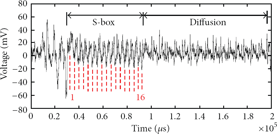
Plot of the EMD trace showing the first ARIA round.
Figure 5 shows the result of the EMD analysis attack on the contactless target card. Figure 5(a) shows the maximum correlation coefficient of each candidate key for the first byte round key. In this result, the correlation coefficients for the incorrect key candidates are significantly smaller than those found for the correct key (0 × D4). The right-hand side of Figure 5 shows the plots for all of the key candidates. 0 × D4 is plotted in black, whereas all the other keys are plotted in gray. There are no significant peaks in gray; only the plot for 0 × D4 contains high peaks.

Result of EMD analysis for the first S-box.
When performing a standard CPA on the EMD signals, we also found all of the 16 bytes round keys from the target contactless card using 50,000 power traces. In Table 1 and Figure 6, we compare the efficiency of the CPA on the EMD signals to that of the CPA on the power signals. To illustrate the comparison results clearly, we define SNR to be the ratio between the correlation of the CPA peak corresponding to the correct key and the highest correlation of the CPA peak resulting from the other wrong keys. In other words, SNR is the maximum correlation of the right key/the maximum correlation of the wrong keys. In this manner, we find that SNR is greater than 1; that is, we can guess the correct key. The greater the SNR is, the higher the accuracy of the round key hypothesis is. As can be seen in Table 1 and Figure 6, all of the 16 round keys could be correctly found with high SNR ratios from both the EMD and the power analyses. With the exception of the 6th and 9th round keys, the experiments show that the EMD analysis gave better results than did the power analysis.
SNR Comparison.


SNR comparison.
6. Conclusions
In this paper, we presented a new side-channel attack that exploited the information leakage from the EMD of a contactless smart card and showed that the EMD can be used as another information leakage channel exploitable in side-channel analysis on contactless smart cards. This novel EMD side-channel analysis allowed for a simple and efficient measurement setup in order to perform side-channel analysis on contactless smart cards.
Footnotes
Conflict of Interests
The authors declare that there is no conflict of interests regarding the publication of this paper.
Acknowledgments
This research was supported by the MSIP (Ministry of Science, ICT and Future Planning), Korea, under the IT/SW Creative Research Program supervised by the NIPA (National IT Industry Promotion Agency) (NIPA-2013-H0502-13-1074) and partly supported by Korea University Grant.