
Abstract
The need for remote monitoring of almost every place in the world is still growing, while many new technical solutions are extensively developed by research community. The knowledge of the environment and the weather conditions of human environment is, in certain cases of polluted places in heavy industrial areas, necessary to allow real-time warnings about deteriorating conditions to living community in these desired places. While huge money investments were used for real-time monitoring of every possible quantity of human body, people's living environment became increasingly poorer. In this paper we present a modern and relatively cheap solution for powering some types of intelligent sensors in which traditional battery power source is insufficient and other powering options are not applicable. Obtaining the energy to supply sensors is possible even from immediate sensors' environment. Sources (which are utilizing thermal gradient) are supplying energy from the surrounding environment and without the need for high-intensity incident light (solar energy based). In order to achieve the full working mode, only a small thermal gradient is needed in order of degrees. The developed test application is using sophisticated electronic circuit provided by Linear Technology Company, which is able to use even small energy bursts for discontinuous intelligent sensors operations. The heat energy is converted into electric energy which is stored in very high-capacity capacitor (about 1 F). This power supply type is suitable for any environment, where some permanent thermal gradient is presented.
1. Introduction
Demands on controlling heating, ventilating, and air conditioning (HVAC) processes in modern multilayer buildings or in the industry are increasing. There are many sensors, which can be used to control given process. However, if we have no sufficient cable infrastructure, these sensors are unusable. Of course, we can use battery-powered smart sensors, but their prize and the need to replace the batteries is constraining. The ideal sensor should have the capability to power itself from the surrounding free energy. This technique is called energy harvesting. Energy harvesting is by no means a new idea. It is a process, by which free ambient energy is derived, captured, and stored. Devices which make use of energy harvesting require output power that ranges from a few nanowatts to tens of milliwatts. Although nontraditional power sources such as solar cells (photovoltaic cells), thermoelectric generators (TEGs), thermopiles, and piezoelectric transducers are known sources of electrical power, harnessing power from these sources has been challenging [1]. Each of these requires some type of power conversion circuit that can efficiently collect, manage, and convert these alternative power sources into a more usable form of electrical energy to power sensors, microcontrollers, and wireless transceivers. Advances in low-power technology are making it easier to create sophisticated power energy management units, which are able to collect small pieces of energy, derive them and store them in high-capacity capacitor.
There are many types of energies, which can be utilized. We can harness vibration energy, solar energy, potential energy, mechanical energy, thermal energy, and many others. One common form of ambient energy is mechanical vibration energy, which can be caused by motors running in a factory, by airflow flowing across a fan blade, or even by a moving vehicle. A piezoelectric transducer can be used to convert these forms of vibration energy into electrical energy, which in turn can be used to power wireless sensors. To manage the energy harvesting and the energy release to the system, the LTC3588 piezoelectric energy harvesting is used for power supply. It uses an efficient energy harvesting algorithm to collect and store energy from high impedance piezoelectric elements, which can have short-circuit currents in order of tens of microamps [2]. The LTC3588 harvests ambient vibrational energy through a piezoelectric element which is its primary application. Common piezoelectric elements are PZT (lead zirconate titanate) ceramics, PVDF (polyvinylidene fluoride) polymers, and other composites. Ceramic piezoelectric elements exhibit a piezoelectric effect when the crystal structure of the ceramic is compressed and internal dipole movement produces voltage. Polymer elements comprised of long-chain molecules produce voltage when flexed as molecules that repel each other. This type of source has one main advantage compared to the other. Output voltage is very high (in comparison to other sources), about 12–25 V. This voltage level is perfect to convert into traditional 3.3 V or 5 V (MCU core and peripherals). Conversion ratio is about 3.5 : 1, so efficiency is high. But supplied power is very low. Typically, harvestable power of this source is in order of tens microwatts. According to (1), if supplied power is low, supply voltage is high, so supplied current is even smaller. This imposes enormous requirements on power/energy management device:
One of the most common energies is thermal environmental energy. Thermal energy is ubiquity, in a relatively large amount. However, there are only few devices which can convert this energy into electric current. One of these is called thermocouples. Thermocouples have been known for a long time. Their main advantage is that they can deliver relatively high current (hundreds mA). But often there is some drawbacks. In this case, supplied voltage is one of the lowest (order of mV). Conversion ratio is about 1 : 50, so efficiency is low. 50 years ago, Russians researchers experimented with kerosene lamps which contain many thermocouples placed on the lamps hat. Resulting power source was able to power simple transistor radio receiver. This type of source has no stabilized output voltage and requires stable heat flow. Also weight, size, and prize of such device cannot be ignored. Modern heat utilizing power sources uses TEGs. TEGs are well accessible, light weighted, and cheap. Low voltage disadvantage is compensated by relatively high supply current and good overall power delivery (hundreds mW). This type of energy has been left out, because the proper switching elements simply have not been accessible. Standard bipolar transistors are not acceptable due to their high Uce-sat (Collector Emitter Voltage in saturation state).
Energy harvesting requires careful power management and sophisticated circuits with latest technology design in order to successfully capture a few microwatts of ambient power and store them in a useable energy reservoir. A capacitor with large capacity usually serves as a reservoir. These electrical devices have been recently revealed. Their capacity, size, equivalent series resistance (ESR), and small leakage current make them perfect to implement into energy harvesting power sources. This capacitor is crucial, because energy is stored after small pulses and, in addition, time between energy deliveries may vary from seconds to minutes. Capacities between 0.1 F and 1 F are recommended and special care must be taken to choose low leakage (about 400 nA) version. Another important device is a switching transistor. Nowadays, special N-MOSFET transistors have parameters, which could not be achieved in the past. A standard bipolar transistor has a very long history and is practically employed on a high level; it has two semiconductor transitions, so minimum switching voltage is about 0.5 V–1 V, which makes it inapplicable in most energy harvesting sources. Modern MOSFET transistors are special electronic elements, which are capable of switching high currents (much more than 100 A) while serial resistance (RDS (on)) remains very low, in order of mOhms [3].
2. Thermoelectric Generators
Thermoelectric generators (TEGs) are simply thermoelectric modules based on Seebeck effect. The Seebeck effect is named after the German physicist Thomas Johann Seebeck (1770–1831), who, in 1826, published the results of experiments done four years earlier that opened up the new field of thermoelectricity. He observed that an electrical current is present in a series circuit of two dissimilar metals, provided that the junctions of the two metals have different temperatures. Devices working based on Seebeck effect convert heat energy into electrical energy where a temperature gradient is present. Sources of heat energy vary from body heat, which can produce tens of μW/cm2 to a furnace exhaust stack where surface temperatures can produce hundreds of mW/cm2. TEGs are basically Peltier cells, running in a reversed mode. The Peltier effect produces a temperature differential by applying voltage and is most commonly used in thermoelectric coolers [4]. These Peltier cells are made from many small semiconductor blocks connected together with copper tape. The most commonly used semiconductor material is bismuth-telluride (Bi2Te3). Output power is directly proportional to the cells' surface and it is directly proportional to the number of semiconductor blocks. The inner structure of Peltier cell is presented in (Figure 1).
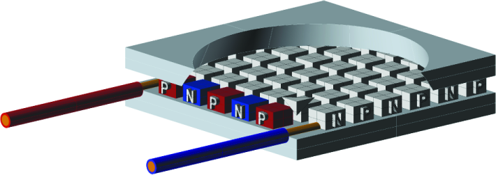
Interconnected semiconductor pellets in TEG module.
TEGs come in a wide variety of sizes and electrical specifications. The most common modules are square shaped, ranging in size from about 10 mm to 50 mm. Their thickness is usually 2 mm–5 mm. We have three types of TEGs (Peltier modules) available.
Most thermoelectric module manufacturers do not provide data for output voltage or output power in relation to differential temperature, which is what the designer of a thermal energy harvester wants to see. Two parameters that are always provided are

Measuring conditions. Heat sinks have been tightened together to ensure best heat flow.
Supposed temperature layout is presented in (Figure 3). The central parts have a linear progression, because the heat perforates through a plain wall. In this area, heat flow depends on the temperature gradient and the heat passage coefficient of all materials which are involved. Individual heat flows can be easily counted according to the following:


Temperature distribution of measured sample.
Heat flow from the heat sink's border into the air has a logarithmic run (Figure 3).
We have made several tests of some commercially available TEGs. The tests were conducted under the same conditions in order for the results to be objective. Temperatures on both sides were recorded and corresponding voltages and passing currents were measured. Supply power was calculated by formula (4). TEG supplies its power into constant load represented by power resistor with value 0R27Ohms. Results can be compared in (Figure 4):


Theoretical electric power delivered by TEGs. Output voltage is in range 50–500 mV.
It can be assumed from (Figure 4) that a cell with a higher nominal voltage (meaning standard supply voltage for normal mode) reports better results. The reason for that is, most probably, the higher count of serial connected semiconductor pellets. Delivered power is only theoretical, because of the high stepup ratio. Total DC/DC efficiency is only between 10 and 50%. Delivered electric power is then between 5 and 100 mW, depending on the input voltage level.
3. Energy Harvesting Management
The basic common feature of the power sources which uses free energy of the surroundings is a discontinuous operation. Many wireless sensor systems require only low average power, which make them front candidates for powering by energy harvesting technique. In addition, many sensors monitor variables with very slow process system type (e.g., oxygen content in water, slow temperature process, and air humidity). Therefore, the measurement can proceed discontinuously, resulting in the low frequency of the cycles and correspondingly low power requirement. If some intelligent wireless sensor make a measurement sample e.g. once per a minute, the average power plummets under 250 μW. This value is significant, because most forms of energy harvesting offer very little steady-state power, so continuous operation is impossible.
As a power management component was chosen, an integrated circuit was provided by Linear Technology, LTC3108. The LTC3108 self-resonant topology steps up from input voltages as low as 20 mV. This energy harvester power source is designed for applications which are using very low average power, but requiring periodic pulses of higher load current (Figure 5). A double-layer capacitor serves as an energy reservoir with large capacity. The recommended capacity is above 0.1 F. Real output power curve can be seen in (Figure 8). The red curve represents output voltage bypassed by 470 uF capacitor, which should align any current spikes. Steady output current is only about 7 mA. The blue curve represents input voltage from TEG, green curve is voltage on supercapacitor, and finally pale blue curve represents useful energy stored in supercap expressed in Ws. As a store capacitor used 1 F sample with 5.5 V maximum voltage and very low leakage current value, maximum storage energy is about 5 Ws. It is big enough to power intelligent wireless sensor, acquire desired data, and send them to superior system to evaluate and subsequent post processing.
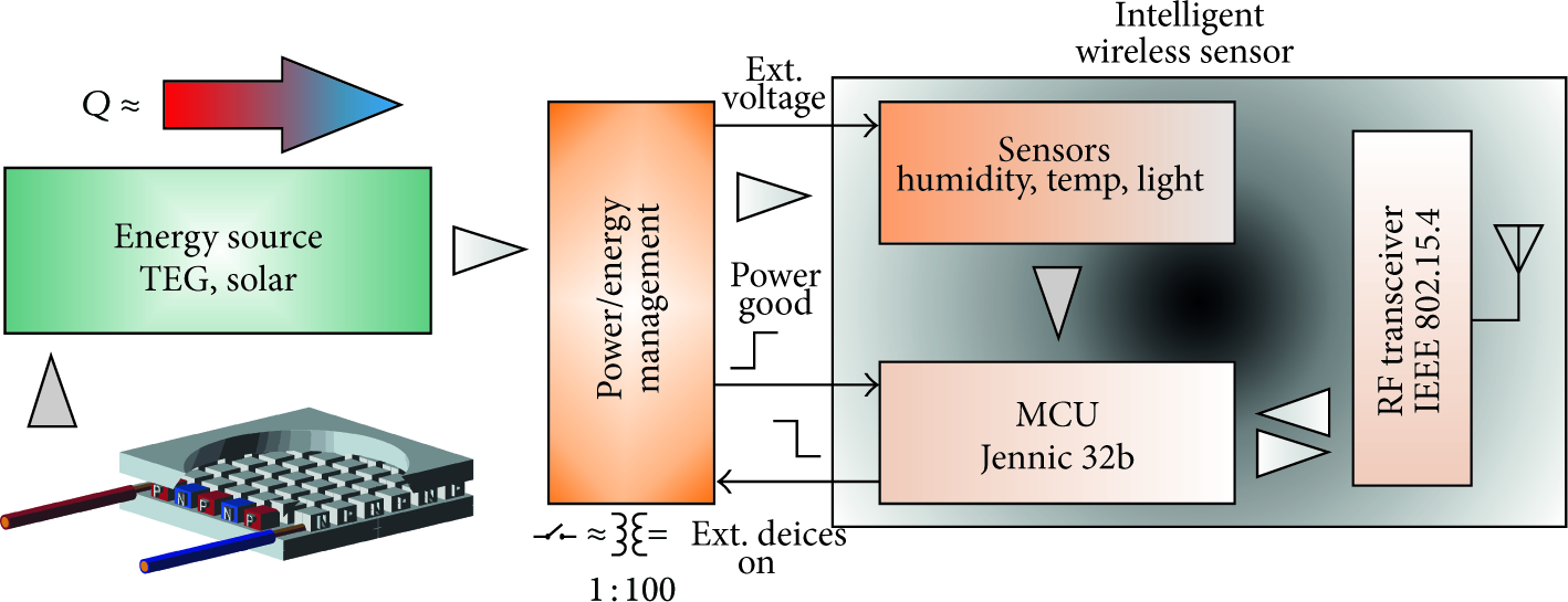
Basic blocks defining powering and measuring chain of independent wireless system.
The accumulated energy can be consequently calculated as follows:

This energy is only theoretical and contains nonutilisable part, because we could utilize only definite voltage range, for example, 3.3–4.0 V. Voltage below the lower limit cannot be utilized (processors core). The useful energy held by capacitor can be calculated as the follows:
The power source with advanced power management IC is presented in (Figure 6). We can see a TEG which is upheld by CIN capacitor to compensate little dropouts. A step-up transformer is designed for the given TEGs output level. The size of this transformer is not essential, because input and output currents are low. Capacitance C1 is the charge pump capacitor that is connected from the transformer's secondary winding to the C1 pin which has an effect on converter input resistance and maximum output current capability. Generally, the minimum value of 1 nF is recommended when operating from very low input voltages using a transformer with ratio of 1 : 100.
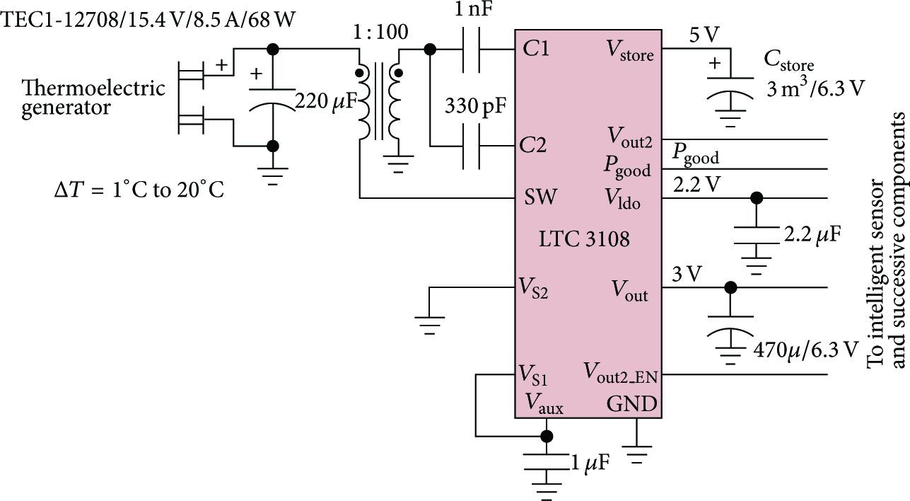
TEG power source for low-input TEGs.
The main advantage of this IC is its ability to start oscillating, even if a very low voltage is applied. The LTC3108 utilizes an MOSFET switch to form a self-resonant stepup oscillator using an external step-up transformer and a small coupling capacitor (C2). This allows it to boost input voltages from 20 mV high enough to provide multiple regulated output voltages for powering other circuits. The frequency of oscillation is determined by the inductance of the transformer secondary winding and is typically in the range of 10 kHz to 100 kHz. Notice
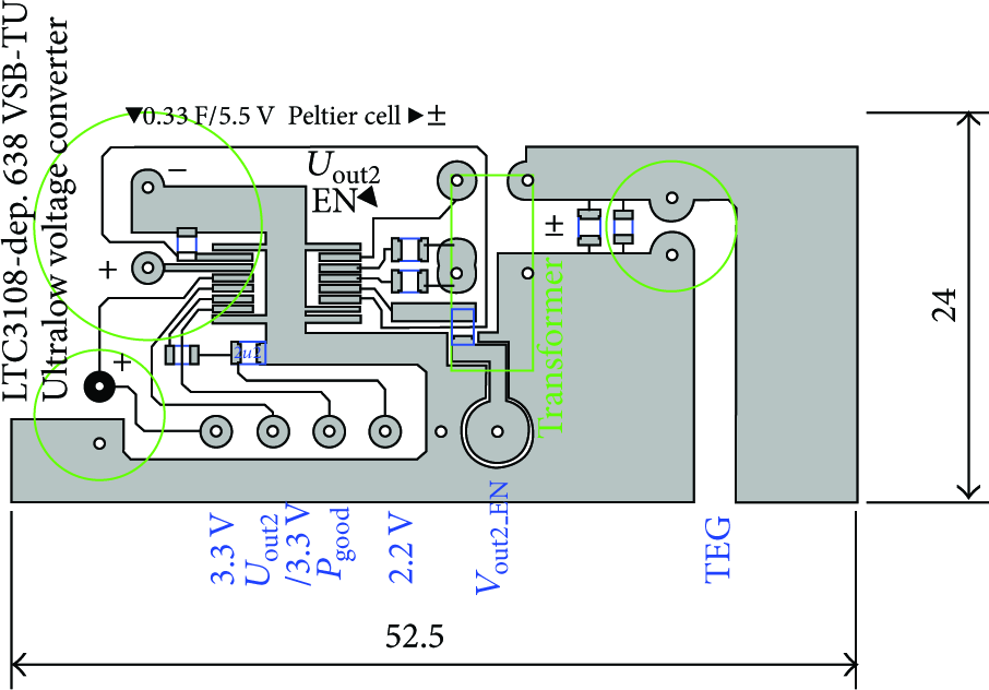
Developed intelligent energy harvesting power source for remote sensors powering (PCB).
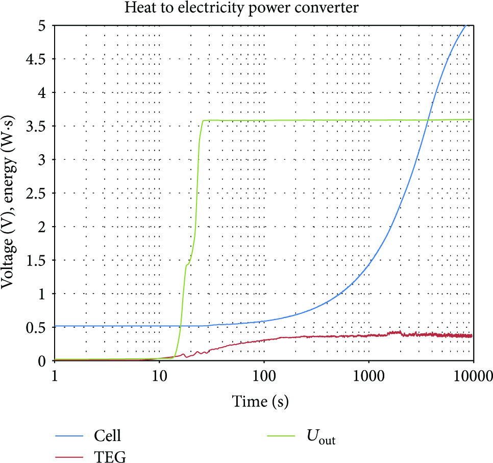
Output voltage running and energy stored in supercap (pale blue).
Real output power curve can be seen in (Figure 8). The red curve represents output voltage bypassed by 470 uF capacitor, which should align any current spikes. Steady output current is only about 7 mA. The blue curve represents input voltage from TEG, green curve is voltage on super capacitor, and finally pale blue curve represents useful energy stored in super cap expressed in Ws. As a store capacitor was used 1 F sample with 5.5 V maximum voltage and a very low leakage current value. Maximum storage energy calculated by (6) is about 5 Ws. It is big enough to power intelligent wireless sensor, acquire desired data, and send them to superior system for evaluate and subsequent postprocessing.
All components were set to optimum device run. Output Schottky diode was strengthened by an external one, so the voltage drop across the diode was lowered. For that purpose was chosen the Schottky barrier rectifier in surface mount (SMD) package with average forward current of 2 A and a maximum reverse voltage of 30 V. Its transfer characteristics are presented in (Figure 9).

Forward current as a function of forward voltage for 5 temperatures from −40°C to 150°C.
As can be seen, for normal temperature of 25°C is forward voltage drop for current in order of mA only 0.08 V. This can significantly improve the whole efficiency, which is very low. A picture from the oscilloscope presents voltage running on this diode. Frequency of 1.898 kHz was used and the oscillogram is shown in (Figure 10).

Oscilloscope output, when measuring rectifier diode forward running.
Small glimmer in the conduction phase forms a transformer core response and is very small due to small transformed energy. These glimmers can be a serious issue if the transformed power is high.
Rectified voltage ripple is 75 mV, which is a relatively good result. Relatively, because the output supply current is very low, in other cases the ripple has tendency to decrease to 0 V. The output ripple is presented in (Figure 11).

Output ripple (yellow line) versus input ripple (red line).
Output ripple is substituted by yellow line and input ripple by red line. Input ripple is significantly lower. This is the sign, that the TEG is very “hard” power supply. Maximum input ripple is about 10 mV, which is partly due to 10 uF ceramic capacitors which bypass the input. The variable switching frequency is visible from the pictures. This is primarily due to the power management unit, which changes switching frequency depending on the input voltage and output power, and also due to primary winding inductance. The inductance of the primary winding is a key attribute when designing target switching frequency. In this case, big core transformer was used, to minimize switching losses (by minimizing switching frequency). The size of the transformer is not important. The goal was to find the possibilities of that type of power supply. On the other hand, the low switching frequency would not interfere any supplying wireless sensors and microprocessors.
In Figures 12 and 13 the voltage running on primary and secondary transformer side is presented.

Switching wave form on primary transformer side.

Switching wave forms on secondary transformer side. The output voltage is 17 times higher than the input voltage.
The two pictures (Figures 12 and 13) show the voltage transformation from input to output. On the primary side, the relatively stable DC voltage with value of 411 mV is presented. When the internal switching transistor accumulates, voltage on the transformer suddenly decreases to almost zero level. This is a sign that internal switch is of a unipolar construction. Then the voltage is starting to increase its value, which is a sign that the switch is not able to maintain passing current and closes itself. This lasts for about 100 us. This time is sufficient to transport low-voltage energy from the input to high-voltage energy on the output. Figure 13 shows that the secondary voltage has a maximum value of about 7.2 V which quickly falls to 5 V. This is due to the used load. Supercapacitors with several farads of capacity have very high internal resistance. Part of the delivered energy is transformed to heat on that resistance and the rest is utilized to increase overall capacitors' charge.
4. Energy Harvesting Power Management—Modern Approach
After many tests, we established that commercial products, such as Linear LTC3108, are suitable for standard, widespread applications. If we want to fit within special conditions such as higher output power, higher charging current, or mixed energy supplies (solar energy + thermal energy), we do not have many options. This area is relatively young and it is still being searched for applications, where this approach could be extensively used.
There are some good journal papers [5–7] that are focused on some of the mentioned problems, but none of them bring the complete solution for optimized power supply. The first one [5] is mainly focused on algorithms to achieve a better system performance as well as lower power consumption. This is certainly needed to be mentioned while developing very low power sensors, but it is not enough in certain cases. This solution is more suitable for more complex measurement cycles.
Some of the interesting solutions can be found in [6] where authors deal with two main options for power sources such as mechanical and electromagnetic energy harvesting, where they also present several circuits' designs. Unfortunately, this issue is not targeted by Peltier cell solution.
The last of the selected solutions deals with a development of a test chip using 180 nm low-threshold CMOS process which results in efficiency of 30%. Unfortunately, this chip is not available in the market now. We assume that the price of this product will be a little higher than the one affordable by our design.
Another paper [8] deals with a supercapacitor with a solar cell combination, but this solution is not possible to be easily used in case of Peltier cells. The major issue arises in a case when we want to charge power supercapacitor quickly, with greater current, which can be delivered by LTC3108. Commercial IC has limitations resulting from its size. In most cases, we have to handle it with small DFN packages, with sizes of about 3 × 3 mm. In this package, the high power, low RDS-ON MOS-FET switch cannot be implemented. Hand by hand with these limitations go other disadvantages. In order to deliver higher input power and larger rectifying diode, larger IC terminals, thicker PCB ways, and others must be used. That is why we design new approach, which has roots in a classic energy harvesting power supply design.
The whole idea is based on ATMEL ATMEGA8 MCU. This MCU has a very low-supply current in active (about 500 μA) and idle mode (about 50 μA). MCU is a driving power MOS-FET with very low RDS-ON (2 mΩ) and high drain current (191A ON state current). This value is excessive and will never be achieved, but other switch parameters are highly suitable for our purposes. Electrical scheme is presented in (Figure 14).

Electrical scheme of intelligent energy harvesting power source.
The major differences compared to commercial products are as follows.
Solution is able to process much higher current than standard energy harvesting device. It can store higher energy. It can use also larger supercapacitors. Output voltage can be controlled by software. It uses CR2032 lithium cell to supply MCU when no input power is present. This prototype is relatively bulky. It can be controlled using UART or SPI interface.
Figure 15 shows a PCB of developed power source. We can focus on several major impact parts. Cell 1 and Cell 2 are high capacity multilayer capacitors supported by two small ceramic capacitors. The main energy part is stored in bulk caps, but they cannot deliver high current spikes. For that reason ceramic capacitors are good supporting choice (very low ESR). Power MOS-FET is placed on the main power path above the JP3 communication connector. Main rectifier schottky diode (D2) is of a bulky type and can carry over 3 A. This value is also unreachable, but on the other hand, due to that, this diode has a very low forward voltage (50 mV/1 A). This can help increase the whole efficiency and maximize input energy utilization.

Intelligent energy harvesting power source (PCB layout and parts overview).
In case that input power is not sufficient to power up MCU, installed lithium battery will ensure the right function. If there is enough input power, output stabilized voltage will pass through separation diode D3 and substitute primary lithium cell. This cell can be replaced by secondary, rechargeable cell. If the input power is too high, there is an LED1 component. Excess energy is then spent in this LED and will not harm any device in the power chain.
5. Discussion about the Contribution for Human Fitness
The presented solution for remote sensors powering is suitable in many cases where we do not need to measure continuous quantities several times per minute, for example, the use of remote sensor networks for monitoring of expansion of oil after sea damage (in Mexican gulf in 2010). For continental areas, a similar usage can be found in monitoring the content of oxygen in fish ponds or lakes in order to be informed about the need to increase oxygen content in water to enable fish to survive in winter periods.
For both mentioned usage areas a 24-hour monitoring cycle is needed. The use of a battery for power in such an HW solution of a remote sensor is uneconomical because there is a need of hundreds or thousands of sensors with a final price of several dollars.
Another example of the application of this solution can be found in monitoring dangerous gas concentration in living environments, monitoring of seismic activities in seismically active places, and oil soil expansiveness in cases of oil tanker accidents. When we are able to precede human contamination (by gas or oil, e.g.), we need to take care of subsequent solution for human disease [9].
It is a paradox that in every industrial manufacture, staff and their working environment are precisely monitored, but when they leave the plant, nobody takes care of them as well as of their living environment. Our solution for remote sensors powering has an ambition to change this trend around.
6. Conclusions
This paper introduced evolving segment of power sources which can utilize free environmental energy, especially thermal energy. Energy harvesting is very quickly penetrating into smart wireless sensor segment. Its advantages are obvious. There is no need to replace or charge batteries which saves time and resources. Placing diagnostics sensors onto places, where standard sensors have no chance, increases safety and can prolong life by early maintenance. Sensing some critical values in large tanks or large water areas can prevent environmental issues. Water environment is especially suitable for heat-based energy harvesters. Relatively constant thermal gradient and high heat capacity of water guarantee good conditions for running sensors array. We can say that energy harvesting is a good option for supplying low power consumption smart sensors for virtually unlimited time [10–15] also in smart cities environments [16–18].
Footnotes
Acknowledgments
The work and the contribution were partially supported by the Project Smart Solutions in Ubiquitous Computing Network Environments, Grant Agency of Excellence, University of Hradec Kralove, Faculty of Informatics and Management and SmartHomePoint Solutions for Ubiquitous Computing Environments, University of Hradec Kralove under the Project no. SP/2013/3. The authors also acknowledge being supported from Cautum Company (![]() ). Last but not least, they acknowledge the technical language assistance provided by Stanislava Horakova (University of Warwick).
). Last but not least, they acknowledge the technical language assistance provided by Stanislava Horakova (University of Warwick).