
Abstract
Seismic sensors are invaluable for intruder detection and perimeter security. In a typical wireless sensor network application of seismic sensors, the units are battery powered and low power consumption becomes critical while fulfilling system requirements. Although many systems utilize 24-bit ADC for seismic signal processing, we employed 12-bit ADC for low power consumption. Because of this relatively low resolution ADC, preamplifier and filters require careful hardware design. We employ bidirectional T-type filtering, noise reduction, and distributed filtering between gain stages before the signal is input to ADC. The proposed design was verified with measurements. Seismic data signals due to footsteps at varying distances were successfully measured.
1. Introduction
Seismic sensors in wireless sensor networks (WSNs) find increasing applications ranging from disturbance detection to critical compound security. Analog design of these sensor boards plays critical role in system performance as geophone sensors generate signal in microvolt's range. When geophone signal is amplified, filtered, and digitized, the data are usually transferred in WSN to a central processing unit. Although the design of wireless nodes has been matured to great extent such that there exist many integrated circuits (ICs) for transceivers, there is little known about the electronic design of the seismic sensor board. This study aims to bridge this gap by analyzing the sensor board requirements and electronic design steps. The design of a wireless node is also presented to fulfill low power requirements but not detailed as this design is relatively straightforward.
Human activities on ground generate vibrations from the point of contact as seismic waves. Seventy percent of those seismic vibrations are transmitted by Rayleigh waves which spread on the surface of the world. The remaining part of that energy is moved by body waves which spread perpendicularly to the Rayleigh waves [2, 3]. In order to detect humans and vehicles, Rayleigh waves can be very useful because of the transmission direction. Those vibrations also have frequency-dependent attenuation characteristics [4]. In addition, ambient environment plays a crucial role in footstep and vehicle detection. For example, because of the increased seismic noise levels, detection distances are lowered during daytimes [5]. The relationship between the noise level and footstep detection distance is further examined in [6]. Another important parameter of the ambient environment is the vibration transmission filter of the ground. Vibration speed in the ground varies depending on the vibration frequency [7]. Footstep and vehicle vibration vary considerably according to these properties of environment and intruders. According to [8, 9], several important parameters of detection are footstep size and speed, shoes of the intruder, seismic noise at the background, unwanted targets, presence of residential buildings, generators, type of ground surface, air condition, geology, and soil conditions. Geophone sensors have several advantages in detecting footsteps and vehicle vibrations as they are less sensitive to Doppler effects of the environment variations than acoustic sensors, have the ability to work with no power (passive), and possess higher detection ranges relative to other sensors [9]. Generally two types of geophone sensors are used: single-axis and three-axis geophones. High bearing estimation error is usually the bottleneck of three-axis geophones. Also path tracking and bearing estimations in critical areas are more difficult by three-axis geophones than triangulation of single-axis geophones because geophone sensitivity is divided along all other axes [10].
Once seismic signal is detected and digitized, wireless sensor node is used to transmit the data for processing or transmitting low-level alarm generation as illustrated in Figure 1. One of the most important aspects of wireless sensor networks (WSN) is its power management. For example, in [11], 7.5 watt NI-PCI-6033E was used to detect footsteps with 16AH-5V battery. Extending systems lifetime without battery replacement is one of the key targets of any WSN. Several researches in WSN focusing on power efficiency were reported in [12–16]. Sensor board with wireless unit was described in [16] but the design lacks details on the amount of amplification, filtering, and noise reduction in the electronics. In this study, we present these details and provide board design with critical circuit components. Our design differs from earlier studies in terms of T-type filtering, noise reduction, and distributed filtering between gain stages before the signal is input to ADC. Low power consumption at every level is the key goal in our design.

Seismic sensors in WSN.
2. Seismic Sensor Hardware Design
Most part of footstep vibration energy is distributed in the band from 10 to 100 Hz [3]. Thus, filters for the amplification of the signal must be of low pass filter type. Geophone sensor generates ultralow amplitude response (in microvolts) to human steps and vehicle movements. For signal processing hardware, the amplitude of geophone sensor signal should be amplified with gain in excess of 1000. Low-level amplifications require high resolution ADC which also induces more noise. A typical geophone sensor is illustrated in Figure 2. Measurements of this sensor using LCR-meter have been carried out and an equivalent circuit as shown in Figure 3 has been formed for the design. The seismic sensor used in our study is SM-24, and its technical specifications are given in Table 1.
Geophone SM-24 technical specifications [1].


SM-24 geophone [1]: (a) representative view, (b) the unit.

Equivalent circuit of SM-24 (measured using LCR-meter).
If we take 12-bit ADC at 3 V full-scale range, then ADC sensitivity is

If amplification of 3000 is used, then 1-bit equivalent voltage at the input of the amplifier is

Hence, the system sensitivity which is the particle velocity that corresponds to one bit of the ADC output is

Therefore, in the absence of noise, a very slight movement in the ground with 8.48 nm/s can be resolved with this amplifier. The maximum value of velocity that puts ADC in its full scale is simply

Seismic sensor noise is mainly thermal noise that produces random voltage fluctuations. The noise voltage is given as
where k is the Boltzman constant, T is temperature (K), B is the bandwidth, and R is the equivalent resistance of the sensor. Using measured equivalent circuit of the geophone with its cable and taking bandwidth 10 Hz as stated in the datasheet, the noise voltage becomes 66.4 μV. Component noise in the amplifiers, Op-amp noise, ADC noise, and power supply noise are all additives to total noise power. Thus, high level common-mode rejection ratio (at least 100 dB) Op-amps should be chosen and input of the amplifier should be noise matched with proper components. Board layout and component choices also play a critical role in the system noise. Power lines are usually the most common source of external noise induced at the sensor input.
System block diagram of the proposed seismic sensor is shown in Figure 4. First, the signal obtained from the sensor is filtered (filter-1) and amplified by 10. Two-stage amplification has the advantage that the same total gain can be obtained with low-value resistors. Thus, noise from resistors is decreased, and signal-noise ratio is increased with filters placed between the amplifiers. The electronic design is detailed in Figure 5. In this design, C5 capacitor removes unwanted offset value due to Op-amps. Another important point of this design is its dual-supply compatibility with wireless unit. ADC input can be easily corrupted due to dual power supply, and to prevent this, D1 diode is used before the buffer block. So, the negative side of the amplified seismic signal is not transmitted to ADC input.

Block diagram of seismic sensor node.

Seismic sensor board schematic.
In high gain amplifier circuits, sometimes sensor signals leak to offset voltage which is generated by voltage reference integrated circuits or voltage dividers. If supply voltage has a DC bouncing or high frequency noises, all offsets would be affected. Because of this, signal from the sensor can be corrupted as well. This is a problem not only for signal processing but also for digital and analog circuits where DC voltage bouncing deteriorates circuit performance. However, it is not easy to eliminate DC bouncing on power lines. Filters on signal lines are used to eliminate high frequency noise only, and careful board layout minimizes the effects of DC bouncing. According to SM-24 geophone sensor, signal frequencies from natural activities would be under 100 Hz. Wireless communication, on the other hand, is implemented at 2.4 GHz. There is a huge frequency difference between signal and the wireless communication frequency. Thus, elimination of high frequency noise is not an issue.
Sharp filtering is also not a requirement for these applications. However, considering other possible noise sources, cut-off frequencies should be selected as close as possible to sensor signal but larger than the Nyquist sampling frequency. By looking at the frequencies, it is obvious that low pass filters must be used on signal lines. These passive components will be critical in general power consumption. Filters are implemented between the Op-amp circuit blocks so that they do not drive any load. However, higher filter input impedance will affect the total gain value indirectly. Directional filters would be more appropriate but difficult to implement. Instead, T-type filters, which have the same cut-off of frequencies in both directions, provide good isolation between the input and the output.
Since filter-1 is the most critical filter in the design, its PSpice simulation is shown in Figure 6. Overall circuit performance is illustrated in Figure 7.

Filter-1 response.

Overall circuit response.
3. Wireless Communication Unit
WSN includes sensor nodes and at least one gateway (gateways can be increased depending on coverage area). There are sensor board, sensor itself, battery box, wireless node, and 2.4 GHz antenna in each sensor node. There is no cable to connect the sensor nodes. They need a battery box for power. They make an alarm decision at the node and send only alarm information to gateway via wireless communication. The signal processing is performed at the node, but signal processing parameters such as duration thresholds, threshold memory sizes, and adjustable gain values at the Op-Amps can be modified remotely through wireless communication link. A typical application is shown in Figure 8.

Typical WSN application.
The nodes automatically choose the most suitable and reliable way of communication for themselves through intercommunication with adjacent nodes. The nodes at both ends of each segment receive such data and transmit them to user by using conventional communication channels. Any gateway acts at the same time as the substitute of any other gateway, and, as it is the case for the detecting nodes, they substitute each other in their function in case of breakdown so that the probability of shut-down of the system due to any failure in any one of the gateways is minimized. Thus, this unique feature is an additional measure against any eventual tactical deception attempts.
The main properties of the two-way communication protocol are sleeping cycles, communication paths, and node-alive query. If an alarm condition occurs at a node, the node tries to deliver the corresponding alarm data to the gateway through other nodes. To reduce communication traffic and power consumption, relevant alarm data is transmitted over private path which is determined inside the node. Also, alternative paths are kept in the node to avoid problems that may arise due to the environment. This hopping technique and keeping backup path also prevent communication breaks against node breakdowns.
Technical specifications of the wireless node based on Texas Instruments (TI) ICs are summarized in Table 2.
Wireless node technical specifications.
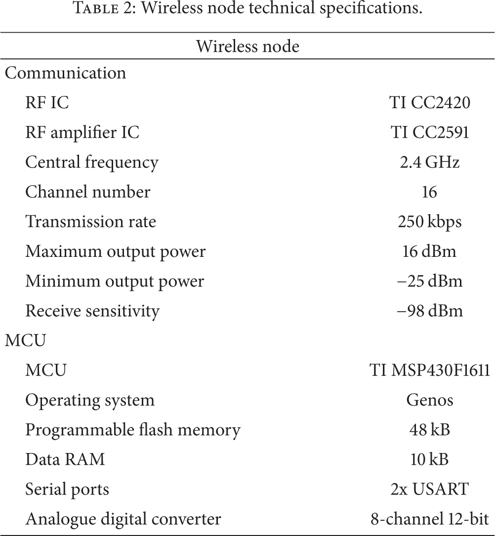
Low power operation of the node is mainly due to the ultralow power microcontroller (TI MSP430 F1611) with 10 kB of RAM, 48 kB of flash, and 128 B of information storage. This 16-bit RISC processor features extremely low active and sleep current consumption that permits nodes to run for years on a single pair of AA batteries. The MSP430 has an internal digitally controlled oscillator that can operate up to 8 MHz. Our wireless node also has a second external crystal (8 MHz) for a more stabilized main clock. The MSP430 has 8 external ADC ports and 8 internal ADC ports. A variety of peripherals are available including SPI, UART, digital I/O ports, watchdog timer, and timers with capture and compare functionality. The F1611 also includes a 2-port 12-bit DAC module, supply voltage supervisor, and 3-port DMA controller.
The CC2420 is an IEEE 802.15.4 compliant radio providing the PHY and some MAC functions and can be controlled by MSP430 microcontroller through SPI port, digital I/O lines, and interrupts. The radio can be shut down by the microcontroller for low power duty cycled operation.
Wireless nodes can be powered by two AA batteries from two different input ports. While one of these inputs has direct connection to the system, the other input has a voltage matching circuit with stabilized output of 3.3 V for an input range of 0.6–3.6 VDC. Wireless node power specifications are given in Table 3.
Wireless node power specifications.

4. Realization and Measurements
The seismic sensor and wireless sensor boards are designed and built separately. The seismic sensor board is shown in Figure 9 where all blocks are labeled. This board is called daughter board and it is interfaced to the main board via 24-pin connector. The whole assembly is shown in Figure 10.

Seismic sensor board.

Whole unit: (a) interior side of the shielded box and (b) actual prototype.
Amplifier 1 output and ADC input of the unit are measured via mixed-signal oscilloscope and the results are displayed in Figure 11. Recorded signal as a function of footstep range is shown in Figure 12.

Oscilloscope measurements of the assembled unit: (a) amplifier-1 output and (b) ADC input.

Footstep amplitude as a function of distance (normalized after 3 K gain).
5. Conclusion
Design of seismic sensor board coupled with a wireless node is detailed. The essential part of the design is its low power consumption due to relatively low resolution ADC. While similar designs utilize much higher resolution such as 24-bit, they consume too much power which makes them less preferable in a battery-powered wireless sensor network application. Our 12-bit ADC implementation requires careful preamplifier and filter designs. System sensitivity and maximum disturbance velocity are calculated. PSpice simulations are run on the design to test the performance of the hardware. Prototypes are built and measured to observe the seismic signals due to footsteps at varying distances, and with as low as 3000 amplification, seismic signals above noise floor due to footsteps can be observed at 15 m.