
Abstract
This paper has proposed an automatic precise alignment coupling algorithm of planar optical waveguide devices based on polynomial fitting, and the experiment shows that for 1 × 8 planar optical waveguide splitter, the time it takes for alignment is within 2.5 min and for 1 × 16 planar optical waveguide splitter, the required time is within 3 min. For 1 × 8 planar optical waveguide splitter, many repeated experiments can guarantee that the insertion loss of the device channels is less than 10.5 dB, with the maximum uniformity of 0.67 dB; for 1 × 16 planar optical waveguide splitter, many repeated experiments can guarantee that the insertion loss of the device channels is less than 13.7 dB, with the maximum uniformity of 0.66 dB. The alignment velocity, precision, and reliability of this algorithm are all greatly increased.
1. Introduction
Planar optical waveguide device is currently one of the key devices of all-optical passive network and optical fiber sensor network, and it can realize functions such as optical beam splitting/combining, switching on and off, and multiplex/demultiplex of optical signals [1, 2]. The core diameter of the single mode fiber is 8∼9 μm, and the optical channel section feature size of the optical waveguide chip is 4∼8 μm, both of which are the dimensions at the micron level. High-quality packaging is premise of its application and cost reduction [3]. Packaging of planar optical waveguide devices makes use of the motion platform of submicron precision to conduct alignment coupling and adhesion joint for optical channels of optical waveguide chip as well as optical channels of input and output fiber arrays. There are 2 methods for alignment coupling, which are active alignment and passive alignment [4]. Passive alignment requires special structure like mask markers, V-groove to realize alignment, and coupling for optical fibers and optical waveguide chip [4]. Active alignment takes advantage of the motion platform of sub-micron precision to realize alignment and coupling for optical fibers and optical waveguide chip by way of optical power feedback, and it is especially fit for automatic operation with assistance from alignment algorithm.
In terms of alignment algorithm, hill climbing is the most widely used one currently. Hill climbing was firstly used in optical axis alignment in 1986, and it was called “gradient search” algorithm at that time [5, 6], which was applied to XYZ axis alignment. Since hill climbing is easy to realize, it is widely used in automatic packaging of optoelectronic devices. Hill climbing is 1D search method, while optical axis alignment requires adjustment for multiple freedom degrees, so in this sense, the method of coordinate alternation will be adopted for hill climbing to complete search for multiple freedom degrees, and its search time increases along with the increase of freedom degree quantity. In addition, since cross coupling inevitably exists on the motion platforms of various freedom degrees, which means that motion at one direction may cause subtle changes in another direction or other several directions, it is easy to fall into local maximum points, and thus it may lead to search failure [7, 8]. The following part proposes application of algorithms such as Hamilton algorithm [7], genetic adaptive optimization algorithm [8], simplex algorithm [9], pattern search algorithm [10], and five-point algorithm [11], and automatic alignment coupling of optical axes. These algorithms have not considered the platform motion characteristics, so it is hard to realize engineering application.
Platform motion characteristics and optimum algorithm characteristics must be taken into account to select precise alignment coupling algorithm of optical fibers and optical waveguide chip in order to reach better effect. Errors like reverse backhaul clearance, ball screw clearance, and so forth are intrinsic characteristics of motion platform, and they are inevitable. Though in the process of precise alignment the optical power value acts as feedback, due to intrinsic characteristics of motion platform, convergence is slow and it is time consuming. So when selecting algorithm, the moving time and commuting time shall be reduced as far as possible.
It can be known that it is desirable to seek better intelligent optimization algorithm, to reduce search time, reduce amount of platform exercise, increase alignment privacy, and increase reliability of algorithm. First in Section 2, the planar optical waveguide devices for coupling theory and polynomial fitting algorithm are deduced. Section 3 makes algorithm simulation analysis on polynomial fitting algorithm. Finally, Section 4 makes experimental study on polynomial fitting algorithm.
2. Coupling Theory and Aligning Algorithm Principle
2.1. Coupling Theory
Alignment coupling of optical fibers and optical waveguide chip requires alignment of both sides by the method of mode field matching, but various errors often cause mismatch of mode field distribution. The reasons for mismatch of mode field distribution are mainly mode field mismatch and geometric alignment error. Mode field mismatch is mainly caused by optical waveguide and optical fiber structure parameters, and it is the internal cause. Geometric alignment error refers to the optical power penalty caused by the fact that the relative position of optical fibers and optical waveguide chip does not reach the optimum alignment state. Geometric alignment error includes horizontal dislocation δ x and δ y , angular deflection α, β, and γ, and longitudinal spacing d, as is shown in Figure 1.

Alignment coupling of planar optical waveguide chip and optical fibers. (a) Single optical channel alignment coupling. (b) Multichannel alignment coupling.
Without regard to the condition of end face reflection, alignment coupling of optical fibers and optical waveguide chip depends on the integral of overlaps of optical waveguide chip channel and optical fiber mode field distribution. Suppose that the mode field distribution of optical waveguide chip channel is ψ w , the mode field distribution of optical fiber is ψ f , and then the coupling efficiency between photonic chips and optical fiber is [12]
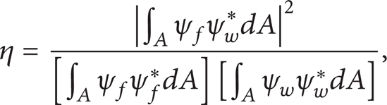
where A is the overlapping area of photonic chip optical channel and optical fiber mode field, as is shown in Figure 2.
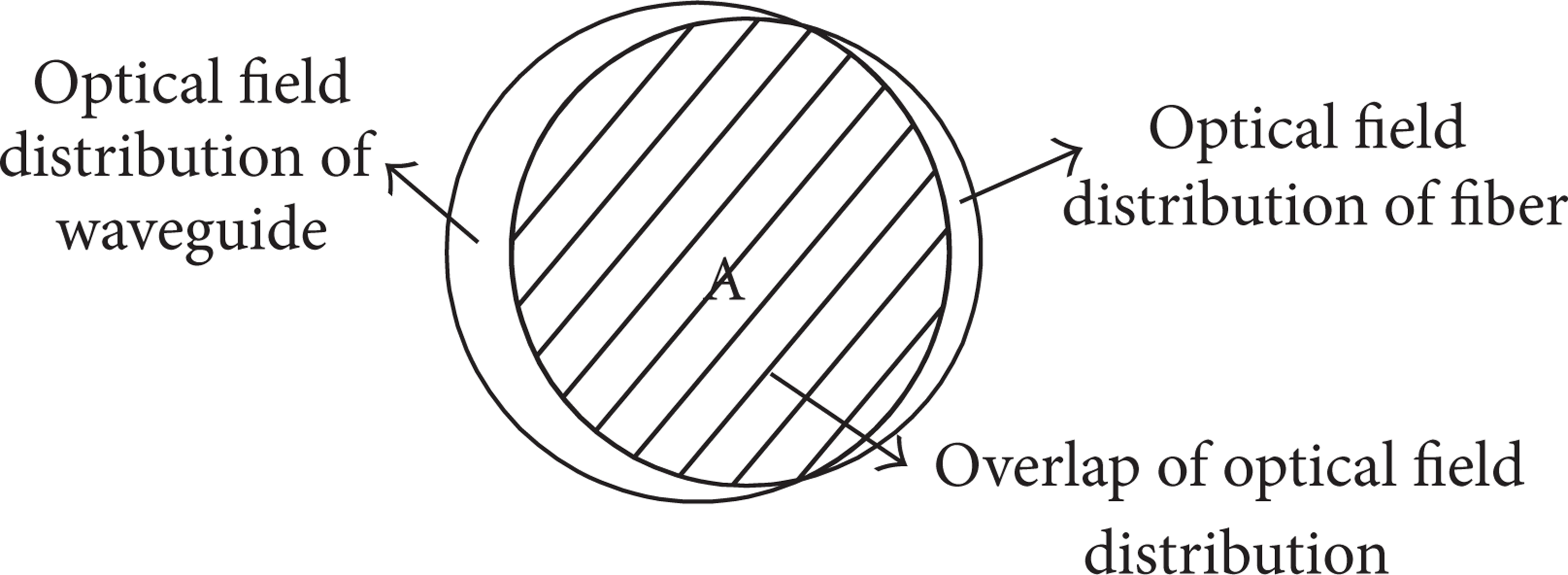
Overlap of optical field distributions between SFM and planar optical waveguide.
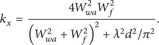
Generally, the mode field distribution of optical waveguide and optical fiber intermediate base can adopt Gaussian function approximation, and error caused by Gaussian beam approximation is no less than 1% [13]. According to [14], the coupling efficiency of optical waveguide and optical fiber is

where


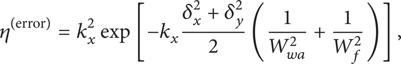
where W f is radius of optical fiber mode field, W wa and W wb are mode field radius of optical waveguide along the ellipse long and short axises, respectively, δ x and δ y are horizontal dislocation, α and β are angular deflection, d is longitudinal spacing, λ is optical wavelength, and z is transmission distance of optical wave. Formula (3) reflects influence of horizontal dislocation, angular deflection, and longitudinal spacing on coupling efficiency. If x is changed into y in formula (3), then the calculation formula of η y (error) can be obtained.
2.2. Aligning Algorithm Principle
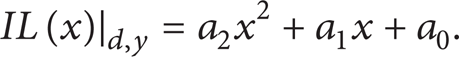
Set α = β = 0, which means that there is no angular deviation between optical fibers and optical waveguide chip; set W wa = W wb , which means that optical waveguide mode field distribution is in a round shape; then, formula (2) can be simplified into
There is no angular deviation between optical fibers and optical waveguide chip, which means that before precise alignment coupling, the angular deviation of α and β among input fiber arrays, optical waveguide chip, and output fiber arrays can be controlled within 0.1° via machine vision technology, and thus, the angular deviation among components can be ignored.
For the given longitudinal spacing d and wavelength λ, k x is a constant. Take logarithm based on 10 of both sides in Formula (5), then multiply by −1, and the following formula can be obtained:

The left side of formula (7) is expression of insertion loss of this optical channel, so theoretically, there is quadratic function relation between insertion loss of alignment coupling of optical fibers and optical waveguide chip and horizontal dislocation. Therefore, by limited data points, the method of polynomial fitting can be adopted to realize rapid alignment coupling of photonic chips and optical fibers to reduce amount of exercise for the platform.
In the horizontal plane XOY, dislocation can be indicated by a vector, which is

The implementation steps of polynomial fitting method are as follows.
Step 1. Set the optical fiber remaining position after rough alignment as reference point P0(x, y) = (0, 0) and the optical insertion loss value of this channel as IL0, and conduct polynomial fitting in the direction of X firstly. Set ILx0 = IL0(x), take 3 points which are P1 (Δx, 0), P2(2Δx, 0), and P3(3Δx, 0) along X axis as distance reference points, monitor the corresponding optical insertion loss value IL1(x), IL2(x), and IL3(x), add the reference point P0, and conduct fitting by the method of least squares for these four points. Suppose that
Set
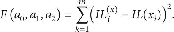
According to extreme value theory, make partial differential for formula (10), set

where a0, a1, and a2 can be obtained, then place them into formula (9), and then the extreme point in the direction of X can be obtained:

Step 2. Move the optical fiber to (x0, 0), monitor the corresponding optical insertion loss value ILy0, take 3 points along the direction of Y just like Step 1, and the extreme point (x0, y0) in the direction of Y can be obtained.
Step 3. Move the optical fiber to (x0, y0), monitor the corresponding optical insertion loss value ILmax0, set this point as new reference point, reduce the step size, and repeat Steps 1 and 2 till the corresponding condition of convergence is met, which means

where k is the iterations and δ and ∊ are optical insertion loss and error allowed in step length, respectively.
3. Algorithm Simulation
According to formula (7), set long and short axis mode field radius of photonic chip optical channel as W wa = W wb = 4.5 μm, radii of optical fiber model field as W f = 4.6 μm, optical wavelength as λ = 1310 nm, and scope of horizontal dislocation δ x and δ y as −5 μm∼5 μm. According to formula (9), it can be known that theoretically there is quadratic function relation between insertion loss of alignment coupling of photonic chips and optical fibers and horizontal dislocation, as is shown in Figure 3.

Relation surface of insertion loss and horizontal dislocation.
Consider the four points which are P1 (1.11, 0.25288), P2 (2.09, 0.89652), P3 (2.39, 1.17240), and P4 (2.68, 1.47410) in the direction of X, as is shown in Figure 4(a). After quadratic polynomial fitting, as is shown in Figure 4(b), the minimum insertion loss of this channel is located in P5 (0, 0). Theoretically, there is quadratic function relation between insertion loss of alignment coupling of optical fibers and optical waveguide and horizontal dislocation, so the extreme value can be obtained by one iterative process in the direction of X.

Quadratic polynomial fit. (a) Data points. (b) Result of fitting.
4. Algorithm Experiment
4.1. System Architecture
Construct automatic alignment coupling system of optical fibers and optical waveguide chip based on Figure 5. The line repositioning resolution of this platform is 0.3 μm, and angle repositioning resolution is 0.001°. Two CCDs and lens are adopted for visual monitor system, with 2 CCD placed vertically and orthogonally, to realize angular alignment and spacing control of input/output fiber arrays and optical waveguide chip. Laser source and two-channel optical power meter are adopted as optical power meter, and they communicates with the computer via GPIB connector.

Structure figure of automatic alignment system.
4.2. Alignment of Optical Fibers and Optical Waveguide Chip
Optical waveguide chips used for alignment coupling are 1 × 8 and 1 × 16 planar optical waveguide splitter chips, and the adhesion used for solid joint of coupling interface is index matching solid adhesion. Table 1 shows the geometric dimensioning and material parameter of planar optical waveguide splitter chips. Refer to Figure 6 for alignment coupling process of optical fibers and optical waveguide chip. Table 2 shows the basic parameters of polynomial fitting algorithm.
Geometric dimensioning and material parameter of planar optical waveguide splitter chips.

Experimental parameters of polynomial fitting.


Process of alignment coupling between planar optical waveguide chip and optical fibers.
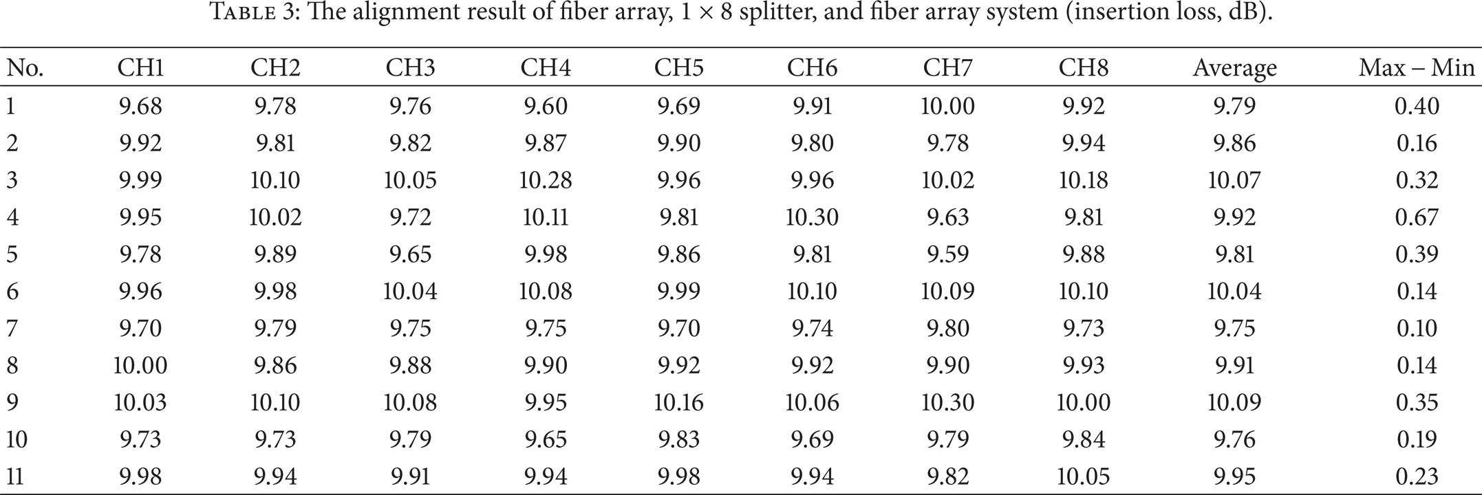
Tables 3 and 4 show the experimental results of alignment coupling algorithm of 1 × 8 and 1 × 16 planar optical waveguide splitters based on polynomial fitting. The theoretical insertion loss of various channels of 1 × 8 and 1 × 16 planar optical waveguide splitters is 9.03 dB and 12.04 dB, respectively, which means that there is only influence of splitting ratio. The extra parts are alignment coupling loss, transmission loss of chip, and so forth. Transmission loss of chips is related to its manufacturing technology and process, it is inherent loss, and generally less than 0.1 dB/cm [1]. Alignment coupling loss is loss caused in the process of device packaging and manufacturing< and is related to motion platform, alignment coupling technology, algorithm, and so forth. For 1 × 8 planar optical waveguide splitter, the time it takes for alignment based on polynomial fitting algorithm is within 2.5 min, and for 1 × 16 planar optical waveguide splitter, the required time is within 3 min. According to Table 3, it can be known that for 1 × 8 planar optical waveguide splitter, many repeated experiments can guarantee that the insertion loss of the device channels is less than 10.5 dB, with the maximum uniformity of 0.67 dB. According to Table 4, it can be known that for 1 × 16 planar optical waveguide splitter, many repeated experiments can guarantee that the insertion loss of the device channels is less than 13.7 dB, with the maximum uniformity of 0.66 dB.
The alignment result of fiber array, 1 × 8 splitter, and fiber array system (insertion loss, dB).
The alignment result of fiber array, 1 × 16 splitter, and fiber array system (insertion loss, dB).
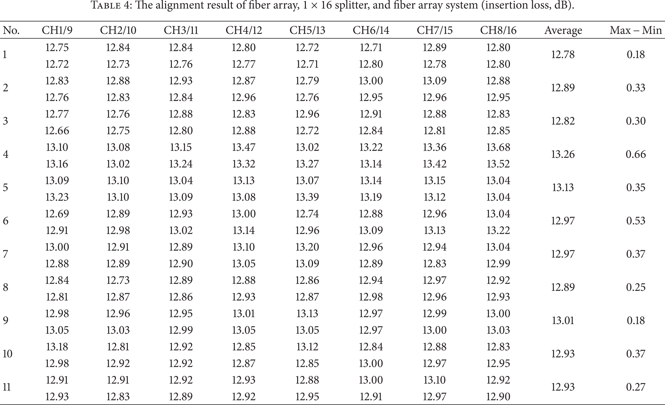
Table 5 shows the experimental results of alignment coupling of 1 × 8 and 1 × 16 planar optical waveguide splitters based on manual stage. The insertion loss is more than 10.5 dB and 13.0 dB, respectively, and the homogeneity index is more than 0.5 dB. The alignment time is more than 5 min. Such results demonstrate the effectiveness of the alignment coupling algorithm which is based on polynomial fitting.
The manual alignment result of fiber array, 1 × 8/1 × 16 splitter, and fiber array system (insertion loss, dB).

5. Conclusion
Automatic precise alignment coupling is the only way of improving optical quality for planar optical waveguide devices, and it is necessary to step into scientific manufacturing from technological manufacturing. Alignment coupling algorithm of planar optical waveguide chip and optical fibers is premise of its automatic packaging, and good alignment coupling algorithm shows in rapid alignment, high precision, and high reliability. This paper has given comprehensive consideration to mode field space distribution of planar optical waveguide chip and optical fibers, motion characteristics of alignment coupling platform, and relation between alignment error and coupling loss and has proposed automatic precise alignment coupling algorithm of planar optical waveguide devices based on polynomial fitting, and the experiment shows that for 1 × 8 planar optical waveguide splitter, the time it takes for alignment is within 2.5 min and for 1 × 16 planar optical waveguide splitter, the required time is within 3 min. For 1 × 8 planar optical waveguide splitter, many repeated experiments can guarantee that the insertion loss of the device channels is less than 10.5 dB, with the maximum uniformity of 0.67 dB; for 1 × 16 planar optical waveguide splitter, many repeated experiments can guarantee that the insertion loss of the device channels is less than 13.7 dB, with the maximum uniformity of 0.66 dB. The alignment velocity, precision, and reliability of this algorithm are all greatly increased.
Footnotes
Acknowledgments
This paper is supported by the National Natural Science Foundation of China (Grants no. 51075402 and no. 50975293), the National High-Tech R&D Program of China (Grant no. 2012AA040406), and the Research Fund for the Doctoral Program of Higher Education of China (Grant no. 20110162130004).