
Abstract
A wireless sensor network consists of low-powered and multifunctional sensor nodes. Since each sensor node is operated by a battery, the energy management has become one of the critical design challenges in wireless sensor networks. Some recent studies have shown that DRAM-based main memory spends a significant portion of the total system power. In this paper, we studied a buffer management scheme for hybrid main memory that combines low-power nonvolatile RAM (NVRAM) and DRAM in order to reduce the energy consumption in a sensor node. Though NVRAMs consume less power than volatile memories, they have common problems in write performance. The proposed scheme employs the page migration technique in order to reduce the write operations on NVRAM part of hybrid main memory. We have performed simulation studies and showed that the proposed page migration scheme outperforms the legacy buffer management schemes in terms of the number of write operations on NVRAM.
1. Introduction
Wireless sensor networks (WSNs) are composed of a number of sensor nodes and are able to perform complex tasks such as monitoring a region to obtain data about the environment and sending data to a central repository station. Today's sensor nodes are full-fledged computer systems, with a processor, main memory, storage, operating system, and a suite of sensors [1–4]. Sensor nodes collect not only sensed data from the environment, but also a stream of mass media data like videos and images. In order to process massive data volumes, sensor nodes are expected to require much more memory than legacy sensor nodes. Each sensor node is operated by a battery, and usually it is not feasible to replace or recharge this battery after deployment. The lifetime of a sensor network is considered over as soon as the battery power of the nodes is completely depleted. Therefore, the energy management of sensor nodes has become one of the key challenges in designing WSNs.
There have been a lot of studies to minimize the energy consumption for WSNs [5, 6]. While most previous studies have dealt with low power communication [7–10], this work focuses on reducing the energy consumption in the main memory in sensor nodes. Sensor nodes use DRAM for main memory as legacy computer systems do. However, recent studies have shown that DRAM-based main memory spends a significant portion of the total system power [11]. Since the capacitors used in DRAM lose their charge over time, DRAM must refresh all the cells approximately 20 times a second, reading each one and rewriting its contents. Such endless refresh operations consume nontrivial amount of power and become a contributing factor for power depletion of sensor node.
The recent advance of memory technology has ushered in new nonvolatile RAM (NVRAM) designs such as PRAM (phase change RAM), STT-MRAM (spin-torque transfer magnetic RAM), and FeRAM (ferroelectric RAM) that overcome the drawbacks of existing volatile memories such as SRAM or DRAM [12–15]. Among the NVRAMs, PRAM and STT-MRAM are becoming promising candidates for main memory because of their high density, comparable read access speed, and low power consumption. Unfortunately, cost per byte of new NVRAMs is extremely higher than that of DRAM until now. As a result, hybrid main memory using DRAM and NVRAM seems to be practicable instead of pure NVRAM-based main memory in the near future. Some recent studies have introduced NVRAM-based main memory organization as follows: PRAM-based main memory organization [16, 17], DRAM/PRAM hybrid main memory organization [18–22], and STT-MRAM-based memory organization [23, 24]. Also, there have been some buffer management schemes for PRAM-based main memory and DRAM/PRAM hybrid main memory [20, 25, 26]. From this research trend, it is highly expected that NVRAM-based hybrid main memory will be used in the next generation sensor nodes soon.
In this paper, we study an NVRAM-aware buffer management scheme for wireless sensor nodes which use DRAM/NVRAM hybrid main memory. Figure 1 illustrates the system configuration considered in this paper. Though NVRAM has attractive features, the write performance (access latency and energy consumption) of NVRAM is not comparable to that of DRAM. The goal of proposed buffer management scheme is to reduce the number of write operations on NVRAM. To do so, the proposed buffer management scheme performs page migration which moves the data from NVRAM to DRAM when the data needs to be written on NVRAM. Furthermore, proposed scheme deallocates clean DRAM buffers eagerly (greedy deallocation) in order to secure free DRAM buffers and thus minimize the number of write operations on NVRAM. We show, through trace-driven simulation, that the proposed scheme outperforms other legacy buffer management schemes in terms of the buffer hit ratio and the number of writes on NVRAM.
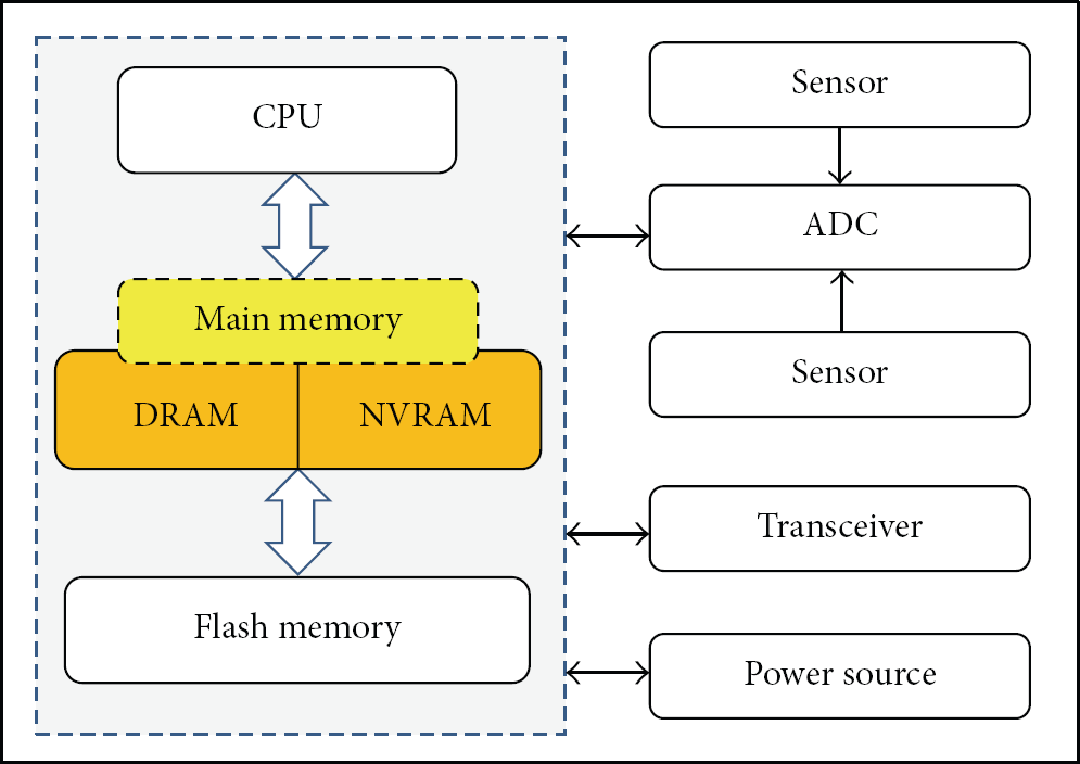
Internal organization of the proposed sensor node.
The rest of this paper is organized as follows. In Section 2, we describe the characteristics of nonvolatile memories such as PRAM, STT-MRAM, and NAND flash memory. Also, we introduce major buffer management schemes which are based on nonvolatile memory. In Section 3, we propose a buffer management scheme called NVRAM-aware buffer (NAB) scheme. It is followed by the description of page migration and greedy deallocation techniques in detail. Section 4 presents the performance evaluation results. Finally, Section 5 concludes the paper.
2. Related Works
2.1. Nonvolatile Memories
Among the NVRAMs, PRAM and STT-MRAM are becoming promising candidates for main memory because of their high density, comparable read access speed, and low power consumption. Table 1 shows the comparison of PRAM, STT-MRAM, and DRAM.
Comparison of memories.

A PRAM cell uses a special material, called phase change material, to represent a bit [12, 27]. The phase change material can exist in two different but stable structural states: amorphous and crystalline, each of which has drastically different resistivity which can be used to represent logic 0 or 1. PRAM density is expected to be much greater than that of DRAM (about four times). Further, PRAM has negligible leakage energy regardless of the size of the memory. While its read performance (latency and energy) is comparable to that of DRAM, its write performance is worse than that of DRAM. Also, PRAM has a worn-out problem caused by limited write endurance (i.e., 108). Since the write operations on PRAM significantly affect the performance of system, it should be carefully handled.
STT-MRAM is a next generation memory technology that takes advantage of magnetoresistance for storing data [13–15]. It uses a magnetic tunnel junction (MTJ), the fundamental building block, as a binary storage. An MTJ comprises a three-layered stack: two ferromagnetic layers and an MgO tunnel barrier in the middle (see Figure 2). Among them, the fixed layer located at the bottom has a static magnetic spin, the spin of the electrons in the free layer at the top is influenced by applying adequate current through the fixed layer to polarize the current, and the current is passed to the free layer. Depending on the current, the spin polarity of the free layer changes either parallel or antiparallel to that of the fixed layer. The parallel indicates a zero state, and the antiparallel a one state.

One of the biggest weaknesses of STT-MRAM is long write latency compared to DRAM. Since the fast access time of memories on a chip must be guaranteed and cannot be negotiable, the slow write operations of STT-MRAM limit its popularity, even though it shows competitive read performance. Another serious drawback of STT-MRAM is high power consumption in write operations.
Flash memory is a sort of nonvolatile memory which has been widely used in storage devices [28, 29]. Unlike PRAM and STT-MRAM, flash memory is a kind of electrically erasable programmable ROM (EEPROM). A flash memory consists of multiple blocks, and each block is composed of multiple pages. A block is the smallest unit of an erase operation, whereas the smallest unit for the read and write operation is a page. Erase operations are significantly slower than the read/write operations. Further, write operations are slower than read operations. Existing data in flash memory cannot be written over; the memory has to be erased in advance in order to write new data. Erase operation degrades the system performance and consumes a considerable amount of power.
2.2. Buffer Management Schemes
There have been a lot of studies on buffer management schemes considering nonvolatile memories [25, 26, 28–33]. In particular, a number of flash memory aware buffer management schemes have been studied over the past decade [28–33]. The goal of these schemes is to minimize the number of erase operations on flash memory. A page-level scheme called clean-first least recently used (CFLRU) was proposed by [32]. CFLRU maintains a page list by LRU order and divides the page list into two regions, namely, the working region and clean-first region. In order to reduce the write cost on flash memory, CFLRU first evicts clean pages in the clean-first region by the LRU order, and if there are no clean pages in the clean-first region, it evicts dirty pages by their LRU order. CFLRU can reduce the number of write and erase operations by delaying the flush of dirty pages in the page cache.
Also, a block-level buffer cache scheme called block padding LRU (BPLRU) was proposed, which considers the erase operations on flash memory [33]. BPLRU maintains an LRU list based on the flash memory block. Whenever a page in the buffer cache is referenced, all pages in the same block are moved to the MRU position. When buffer cache is full, BPLRU scheme evicts all the pages of a victim block but it simply selects the victim block at the LRU position. In addition, it writes a whole block into a log block by the in-place scheme using the page padding technique. In page padding procedure, BPLRU reads some pages that are not in the victim block and writes all pages in the block sequentially. The page padding may perform unnecessary reads and writes, but it is effective because it can change an expensive full merge to an efficient switch merge. In BPLRU, all log blocks can be merged by the switch merge, which results in decreasing the number of erase operations.
For the DRAM/PRAM hybrid main memory, a multiple queue scheme (we call it 4Q scheme) was proposed [25]. 4Q maintains a page list by LRU order and evicts a page from LRU position. In order to reduce the writes on PRAM, 4Q predicts the page access pattern and migrates pages to DRAM or PRAM according to the access pattern. 4Q dynamically moves the write-bound pages from PRAM to DRAM and moves the read-bound pages from DRAM to PRAM. For prediction of the access pattern, 4Q calculates the weighting values of each page at every request and maintains 4 types of monitoring queues (see Figure 3). 4Q shows good performance when the access pattern is highly skewed like financial workload. Though 4Q tries to reduce the number of write operations on PRAM, it does incur high run-time overhead.

Monitoring queues of 4Q scheme [25].
3. NVRAM-Aware Buffer Management
We propose a buffer management scheme called NVRAM-aware buffer (NAB) for wireless sensor nodes which use DRAM/NVRAM hybrid main memory. Figure 1 illustrates the system configuration considered in this paper. The goal of the proposed scheme is to reduce the number of write operations on NVRAM.
3.1. Buffer Page Management
We assume that the main memory is divided into DRAM and NVRAM by a memory address. A portion of main memory is reserved for use as buffer. The buffer space is divided into a set of pages, each of which is a unit of buffer allocation/deallocation. The size of a page is fixed (i.e., 1 Kbytes).
The proposed NAB scheme maintains allocated pages as a page list by least recently used (LRU) order shown in Figure 4. The NAB defines a search region as a set of pages from the LRU position of the page list. When a new page needs to be allocated for storing data, the NAB allocates it from the free buffer pool and stores the data in it. And then, the NAB places it at the most recently used (MRU) position of the page list. Whenever a page in the page list is accessed, it is moved to the MRU position. When a page is deallocated, it is removed from the page list and returned to the free buffer pool.

List-based buffer page management.
In Figure 4, there are 6 pages in the page list. The gray pages are allocated from NVRAM and the white pages are allocated from DRAM. The search region size is 3 pages.
3.2. Page Migration
In order to reduce the number of write operations on NVRAM, when a clean (i.e., not modified) page in the NVRAM is referenced by a write operation, the NAB performs the page migration procedure as shown in Algorithm 1.
if (free DRAM page exists) allocate a DRAM page; perform write to the DRAM page; free original NVRAM page; else if (clean DRAM page exists in search region) free it and allocate a DRAM page; perform write to the DRAM page; free original NVRAM page; else perform write to the original NVRAM page; place the page at MRU position of the page list;
First, the NAB tries to allocate a free DRAM page and writes requested data to the allocated DRAM page. Then it deallocates the original NVRAM page. In Figure 5, for example, data D0 in a NVRAM page is accessed by write request. Then the NAB allocates a free DRAM page and migrates the new data D0 to the newly allocated DRAM page. And then the NAB places it at MRU position of the page list.
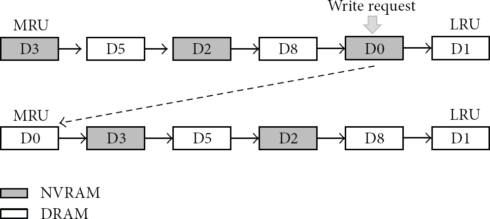
Page migration when write occurs.
If there is no free DRAM page in the free buffer pool, the NAB tries to find a clean DRAM page from the search region and uses it for storing the requested write data. If there is no clean DRAM page in the search region, the NAB writes requested data to the original NVRAM page.
3.3. Page Deallocation
The NAB proposes a greedy deallocation technique which frees clean DRAM pages even though free buffers are still available in the system. Because there could be a lot of used buffers that will not be accessed soon, we can free them early with little influence on the cache performance. To do so, the NAB searches clean DRAM pages from the search region periodically or whenever the number of free DRAM pages falls down below a threshold. Then, it makes them free. This scheme results in decreasing the number of writes on NVRAM because the NAB can secure free DRAM pages for new page allocations.
If all free pages are used up, the NAB selects a victim page from the search region in order to make free pages. In order to reduce the number of write operations on flash memory, the NAB tries to find a clean page. If there is no clean page in the search region, the NAB just selects a page at the LRU position of the page list. If necessary, the data in the victim page is stored in the storage (flash memory).
4. Performance Evaluation
4.1. Experiment Setup
In order to evaluate the proposed scheme, we have developed a trace-driven simulator. For the workload, we obtained the virtual memory traces of an application which is similar to database applications.
For example, TinyDB is a distributed query processor that runs on each of the nodes in a sensor network [4]. TinyDB runs on the Berkeley mote platform, on top of the TinyOS operating system [3]. Using sensor data management functionalities, users connect to the sensor network using a workstation or base station directly connected to a sensor designated as the sink. Aggregate queries over the sensor data are formulated using a simple SQL-like language and then distributed across the network. Aggregate results are sent back to the workstation over a spanning tree, with each sensor combining its own data with results received from its children.
We set the DRAM-to-NVRAM ratio as 1 : 1 and the search region size as 1/3 of the page list. We evaluate the buffer hit ratio and the write counts on NVRAM with varying the buffer size until the buffer hit ratio becomes 100%.
4.2. Buffer Hit Ratio
Figure 6 shows the comparison of buffer hit ratio with varying the buffer size. All schemes except Q4 are similar. When the buffer size is small (i.e., 10), the buffer hit ratio of Q4 is nearly 5% smaller than those of other schemes.

Buffer hit ratio.
However, as the buffer size increases, the buffer hit ratios of all schemes increase rapidly and reach almost 100%.
4.3. Write Counts on NVRAM
Figure 7 shows the comparison of write counts on NVRAM. As the buffer size increases, the write counts on NVRAM decreases. Also, we can see that NVRAM-aware schemes such as Q4 and the NAB outperform other schemes. But, the write counts of NAB decreases faster than that of Q4 as the buffer size increases. Therefore, proposed NAB scheme outperforms all other legacy schemes in terms of the write counts on NVRAM.

Write counts on NVRAM.
4.4. Effect of DRAM-to-NVRAM Ratio
Figure 8 shows the write counts on NVRAM when the ratio of the size of DRAM to the size of NVRAM varies. We set the total buffer size as 500 pages. It is normal that the write counts on NVRAM increase as the ratio of NVRAM size increases. However, the write counts of NAB are smaller than those of other schemes for all cases. Hence, the proposed NAB scheme outperforms legacy buffer schemes regardless of the DRAM-to-NVRAM ratio. The evaluation results of buffer hit ratios are not shown because they are similar to Figure 6.

Write counts on NVRAM.
5. Conclusion
The power of wireless sensor networks lies in the ability to deploy large number of sensor nodes that assemble and configure themselves. A sensor node is a battery-powered computer. If power is used naively, individual nodes will deplete their energy supplies in only a few days. In contrast, if sensor nodes are very spartan about power consumption, months or years of lifetime are possible. Hence, the energy management of sensor nodes has become one of the key design challenges in WSNs. While there are many studies about energy management for low power communication, there have been few researches on low power main memory using NVRAMs in sensor nodes.
In this paper, we study a buffer management scheme for sensor nodes which use NVRAM-based hybrid main memory. Though NVRAM is attractive in terms of power consumption and read performance, the write performance (access latency and energy consumption) of NVRAM is worse than that of DRAM. The proposed buffer management scheme employs a simple page migration technique which migrates the data from NVRAM to DRAM when the data needs to be written on NVRAM. Further, in order to secure free DRAM buffer, the proposed scheme employs a greedy deallocation technique that deallocates clean DRAM buffers even though free buffers are still available in the system. The proposed page migration scheme exhibits better performance than legacy buffer management schemes in terms of the buffer hit ratio and the number of writes on NVRAM. The proposed scheme can be used when DRAM/NVRAM hybrid main memory is adopted in sensor nodes in the near future.
Footnotes
Acknowledgments
This research was supported by Basic Science Research Program through the National Research Foundation of Korea (NRF) funded by the Ministry of Education, Science and Technology (2010-0021897). The author would like to thank Soohyun Yang who helped in the simulation experiment.