
Abstract
This paper presents the design, analysis, fabrication, and characterization of an electrostatically driven single-axis active probing device for the applications of cellular force sensing and materials characterization. The active microprobe is actuated by linear comb drivers to generate the motion in the probing direction. Both actuation and sensing comb-drive structures are designed for the probing stage. The sensing comb structures enable us to sense the probe displacement when the device is actuated, which enables applications of force-balanced sensing and provides the capability of closed-loop control towards better accuracy. The designed active probing device is fabricated on a silicon-on-insulator (SOI) substrate with a 10 μm thick device layer through surface micromachining technologies and deep reactive-ion etching (DRIE) process. The handle layer beneath probe stage is etched away by DRIE process to decrease the film damping between the stage and the handle wafer thus achieving high-quality factor. The fabricated stage provides a motion range of 14 μm at actuation voltage of 140 V. The measured natural frequency of the stage is 1.5 kHz under ambient conditions. A sensitivity of 6 fF/μm has been achieved. The proposed single-axis probe is aimed at sensing cellular force which ranges from a few nano-Newton to μN and micromanipulation applications.
1. Introduction
Different from many engineering materials, living cells exhibit much more complex functions by sensing external stimuli, such as mechanical force, electrical field, chemical and density gradient, and converting them into biological reactions. Research on mechanics of cells has attracted much attention and progressed very fast during past decade for the reason that mechanical loading of cells in forms of deformation and remodelling is known to have significant impact on disease detection and human health [1]. Moreover, study of mechanics in cells and subcellular component is critical for understanding the interaction between mechanical signals and biological behaviours such as cell growth, proliferation, and differentiation. Since cellular and subcellular forces usually range from sub-nN (10−9 N) to μN (10−6 N) [2], high force sensitivity and high positioning resolution are generally required for cell manipulators and cellular force sensors.
Conventional techniques for sensing and manipulating cells include atomic force microscopy (AFM) [3], magnetic twisting cytometry (MTC) [4], piezoresistive and piezoelectric force sensor [5, 6], and capacitive cellular force sensor using transverse comb drives [7]. Among these approaches, AFM has been widely used to study various behaviors and mechanics of cells, like elastic and viscous behavior of muscle cells [8] and cellular strain distributions [9]. However, several limitations restrict AFM's use in cellular force sensing and cell manipulation. The AFM instrumentation uses optical photodiode to detect cantilever deflection [10], which requires complex setup and calibration for their operation and manipulation. The force measuring range is constrained by cantilever properties and conditions, because the photodiode can only detect small deflection. Moreover, operation of an AFM in aqueous cell cultural medium further increases its difficulty in cell manipulation and force sensing, since the reflection and refraction of the laser can degrade the sensing accuracy when the cantilever is immersing inside the aqueous medium.
To overcome the drawbacks of AFM, microelectromechanical systems (MEMSs) technology has been applied in cell manipulation and force sensing and shown great potential in miniaturizing the overall size of the measurement system while maintaining high sensitivity and high resolution. MEMS-based microgripper is reported to be able to provide nano Newton force-controlled manipulation of cells [11]. Passive MEMS force sensors were fabricated and utilized to study mechanical response of cells [12–16], in which lateral indentation force response of single living cells was measured. Through microfabrication process, the size of the sensor is significantly reduced to millimeter level. However, the probe itself is driven by an external piezo actuator, acting as a passive open-loop system. Moreover, the accuracy of force measurement depends on the resolution of optical microscope and CCD camera, since the sensing of force is estimated from the displacement between measurement point and reference point on their device which is acquired and measured through microscope. This measurement scheme also limits its operation only to lateral direction.
This paper presents an electrostatically actuated single-axis active probe. In this design, one of three pairs of linear comb drives provides linear actuation in the probing direction. The other two work as capacitive sensors for displacement/force sensing. The actuation comb drives along with sensing comb drives can provide well-controlled system with higher accuracy and stability, when compared with parallel plate actuators. Meanwhile, since capabilities of manipulation and sensing are fully integrated into one single device, the device can be operated at a variety of environments and at different probing orientations. The small probe tip design also enables us to manipulate cells that are cultured in complex substrates, like 3D scaffold and microgrooves, which is difficult to be accessed by an AFM cantilever. The device structure is designed to be truss-like in order to reduce overall mass and increase stiffness [17, 18]. The device is fabricated on a silicon-on-insulator (SOI) die with a 10-μm-thick device layer and a 2-μm-thick buried oxide layer. Deep reactive-ion etching (DRIE) process is applied to form high-aspect-ratio device structures. The handle layer beneath the device is etched away to facilitate the interaction between the probe and the tested sample and prevents potential stiction issues between device and handle layer. A capacitance IC circuit is integrated with the fabricated MEMS device to obtain precise measurement of the displacement and resulting force to be sensed. The device design and analysis, and experimental test results are presented in following sections.
2. Device Design and Analysis
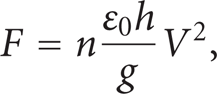
Figure 1 shows the design of the single degree-of-freedom active probing device. In this device, the probe tip with radius of 1 μm is connected to a comb-drive actuated single-axis stage. The motion stage is designed with three sets of comb-drives and is suspended by two pairs of folded springs. Among the three sets of comb-drives, one is used for actuation and the other two are designed as the capacitive sensors to sense the displacement and interaction force. When an actuation voltage is applied to the comb-drive electrodes, the electrostatic force drives the probe stage moving along the probing direction. By calibrating the unloaded voltage-displacement relationship, and comparing it with the measured displacement when the external load is presented during the probing application, the force-displacement relationship of the tested sample can be derived.
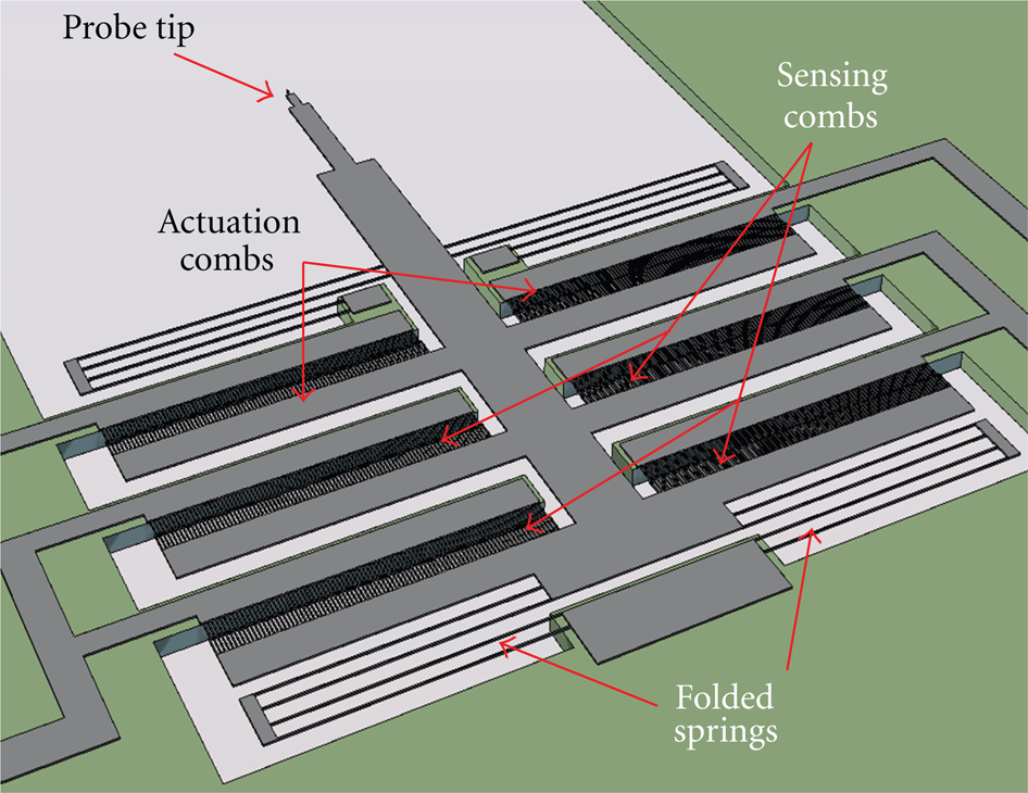
Schematic diagram of the active probe device with actuation and sensing combs.
The maximum displacement of the probe stage is defined by the stiffness of the overall device structure and the actuation force generated by comb-drive actuators. In this device design, two types of folded springs are used as suspension structures (Figure 2). The designed folded spring has a large compliance in the actuation direction for large displacements and a much higher stiffness in the lateral direction so as to prevent lateral instabilities. According to the beam deflection theory [19], the stiffness of a doubly clamped beam in the motion direction and lateral directions can be expressed:
where k x and k y are the stiffness of the clamped-clamped beam in X (lateral) and Y (motion) direction, respectively, E is the Young's modulus of the beam material, h is the height of the beam, t is the thickness of the beam, and L is the length of the beam. The stiffness ratio is

The stiffness ratio of the designed folded spring needs to be very high so as to prevent side instabilities.

Schematics of two types of springs (a) the top spring and (b) the bottom spring.
In our folded spring design, the folded spring that locates closer to the long probe is consisted of two clamped-clamped beams with different length in series (Figure 2(a)). The lower beam connects the anchor to an intermediate truss and the upper beam connects the truss to probe stage. The stiffness expressions of the upper beam and the lower beam of the top spring are, respectively, given by

Here, Young's modulus of silicon (E) is 130 GPa, the height of the beam (h) which is equal to device layer thickness is 10 μm, the width of the spring beam (t
t
) is 17 μm, the length of the upper beam (
Since the upper beam and the lower beam are in series, the overall stiffness of this folded spring (k t,x for X direction and k t,y for Y direction) can be obtained through the beam deflection theory mentioned above:

We obtain the stiffness values for the top spring as k t,y = 2.18 N/m and k t,x = 24762 N/m.
The other set of folded spring is located at the bottom of the probe stage (Figure 2(b)), in which the beams have the same length. The stiffness of this folded spring (k b,x for X direction and k b,y for Y direction) can similarly be expressed as:
where the width of the bottom spring beam (t b ) is 15 μm and the length of the bottom spring beam (L b ) is 1.6 mm. We obtain the stiffness values for the bottom spring as k b,y = 2.14 N/m and k b,x = 24375 N/m.
The two folded springs are in parallel configuration. Therefore, the total stiffness in X and Y directions of the probe stage can be determined by

Thus, the total stiffness in the motion direction is 4.32 N/m and in the lateral direction is 49137 N/m, resulting in a high stiffness ratio of
The comb-drive actuator provides actuation force to deflect the folded springs and generate motion of the probe stage in Y direction. The electrostatic force generated by comb drive under actuation voltage, V, is given by
where ε0 is permittivity of free space. In this design, the number of the fingers in actuation comb drive (n) is 176, and the gap between two neighboring fingers (g) is 5 μm. Hence, the comb drive can generate a 61 μN force under actuation voltage of 140 V.
For displacement and external force sensing, two pairs of comb drives are designed as the capacitive sensor to sense the displacement and interaction force. The number of the sensing fingers (n
s
) in comb drive is 352. Under ideal condition when parasitic capacitance is negligible, the capacitance change (

Thus,

We have
3. FEA Structural Analysis
To verify the device design from the above section, static analysis of the probe stage is performed through finite-element analysis (FEA) method (using Comsol). A 3D model is generated by AutoCAD and processed with Comsol. Due to node/memory and computing capability limitations, the truss structure of the moving parts of device is replaced by solid geometry and comb-drive fingers are removed from the model. To compensate for the extra mass introduced by the simplification, the material density of the moving parts is scaled down appropriately. Figure 3(a) shows a 2D model of the probe stage in both original state and deformed state under an actuation force. Different color indicates the different displacement in μm. In the FEA simulation, a force of 61 μN is applied to the probe stage and a displacement of 14.5 μm is achieved. Thus, from FEA simulation, we obtain a stiffness of 4.21 N/m (=61 μN/14.5 μm) which fits very well with theoretically analyzed result of 4.32 N/m.
(a) FEA static analysis of the probe stage displacement. (b) Device sagging due to self-weight.
Since the probe device has a long suspension structure, out-of-plane sagging of the device due to its own weight can cause problems in its actuation and sensing. It can lead to the twisting of the leaf springs, misalignment between the comb fingers, and affect the orientation of the stage. Thus it is necessary to check the self-sagging of the device through FEA. A surface load corresponding to the weight of the structure is applied to the top surface of the device to make it equivalent to the gravity load. The result of FEA analysis is shown in Figure 3(b). The simulation indicates that the maximum sagging of the structure (at the tip of the probe) is only 500 nm. Compared with the overall dimension of the device (5 mm), the sagging effect is negligible. Moreover, considering the actuation of the device (in-plane direction), the out-of-plane mode will get much less chance to be excited in the real operation, since no actuation energy is given to this mode. Thus in our dynamic FEA analysis, we focus on the eigenmodes in xy-plane.
The dynamic behavior of the probe stage is analyzed by FEA as well. Figure 4 shows the first-six mode shapes and their corresponding natural frequencies. The deformations in these plots are scaled up for better demonstration. Among these modes, only Mode 1 with natural frequency of 1.38 kHz is related to the desired motion of the probe stage. The modes other than Mode 1 show localized vibration in spring beams, not contributing to the actual operation of the device. The natural frequency of Mode 2 is 8 times higher than that of Mode 1, hence indicating 64 times stiffer than Mode 1, which provides a good separation between the modes associated with desired motion and those associated with parasitic motions.

Six modal shapes and their corresponding natural frequencies.
4. Device Fabrication
The fabrication process flow of the device is demonstrated in Figure 5. The process includes two patterning and two DRIE etching steps. We use two photolithography masks to transfer desired patterns to device layer and to handle layer. The device is fabricated on silicon-on-insulator (SOI) wafer with device layer thickness of 10 μm, buried oxide (BOX) layer thickness of 2 μm, and handle layer thickness of 500 μm. The 4-inch SOI wafer is diced into 15 mm × 15 mm dies. The SOI substrate allows for the two parts of the electrostatic linear comb drives (fabricated on the device layer) to be electrically isolated from each other (by the BOX layer), while being structurally supported by the handle layer. The size of the device, without the contact pads, is about 5 mm × 4.5 mm.

Fabrication Sequences. (a) Starting from a SOI substrate; (b) device layer (Stage) patterning; (c) handle layer patterning; (d) handle layer through etching by using the Bosch process (DRIE); (e) removal of the BOX layer using HF (49%); (f) device layer DRIE etching; (g) Al etch mask removal.
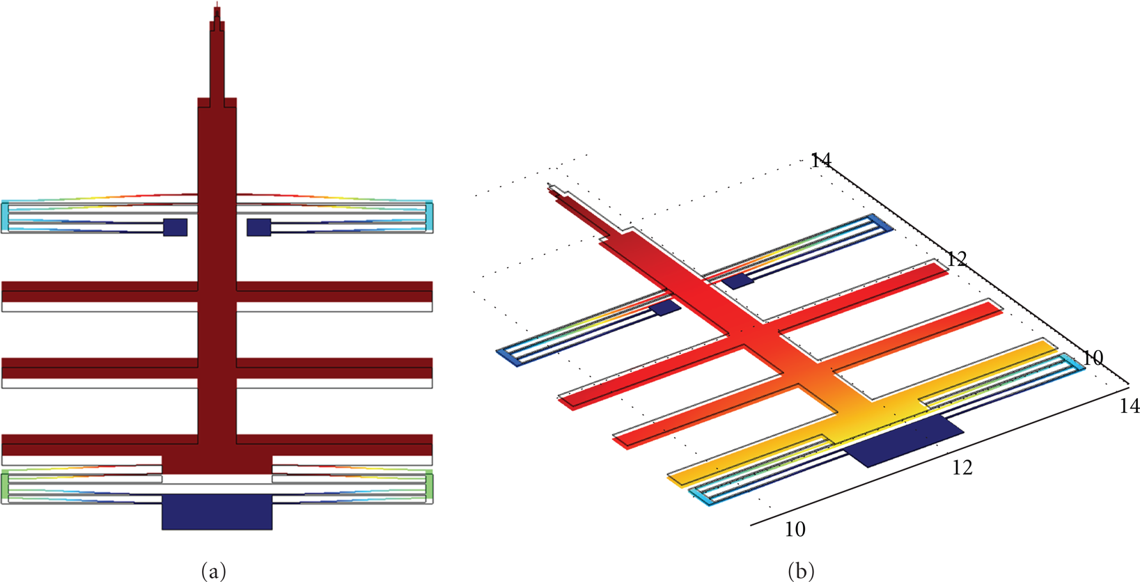
The microfabrication process begins with the cleaning of the pieces from the diced wafer. The cleaning step serves to remove the debris, particles, and organic contamination after dicing (Figure 5(a)). Ultrasonic cleaning is performed sequentially in acetone, isopropyl alcohol (IPA), and methanol, followed by 1-minute dehydration baking. The front-side device pattern is patterned on the device layer of the SOI die by process of photolithography using photoresist S1813. After photoresist is patterned on the device layer, evaporation process of aluminum is performed. A 150-nm-thick aluminum layer is deposited on the device layer, followed by lifting off in an N-methyl-2-pyrrolidone (NMP) bath through ultrasonic cleaning (Figure 5(b)). Before the handle layer is patterned, photoresist S1813 is spin coated and hard baked on the device layer side to protect the front side for subsequent processing. Patterning of the handle layer follows the same patterning process with which the device layer is patterned (Figure 5(c)). A 200 nm thick aluminum layer is deposited on the handle layer. The evaporated aluminum film is used as etching mask during DRIE process. The patterned handle layer is then etched by the BOSCH process using the Alcatel AMS 100 Deep Reactive Ion Etcher. A high-etching-rate recipe is used for backside etching with 1.5 seconds C4F8 passivation cycle and 8 seconds SF6 etching cycle. A 1.5-hour etching is performed to remove the handle layer silicon beneath the moving part of the device which is 500 μm. The etching stops on the BOX layer (Figure 5(d)). The BOX layer is then removed through a wet-oxide etching process using concentrated HF (49%) (Figure 5(e)). HF is carefully dropped on the BOX layer without flowing onto the front side, which prevents HF from etching the Al mask on the front side. Following the removal of the BOX layer, the device layer is then etched by the BOSCH process with a low-roughness recipe. The BOSCH process recipe is optimized to yield a smooth sidewall with high aspect ratio with 1 second C4F8 passivation cycle and 3 seconds SF6 etching cycle. A 4.5-minute etching is performed on the device layer till the device layer is fully etched through(Figure 5(f)). After an optional step to remove the aluminum mask in aluminum etchant, the device is ready to be tested (Figure 5(g)). Scanning electron microscope (SEM) images of the fabricated device is shown in Figure 6. Due to the limited field of view, the probe tip is not displayed in overall structure image in Figure 6(a), but close view image of the probe tip is given in Figure 6(c). Figure 6(b) shows a close view of comb fingers.
SEM images of the fabricated device: (a) overall stage (probe tip is not displayed); (b) close view of comb fingers; (c) top view of the probe tip; (d) side view of the probe tip.
5. Characterization and Test Results
After fabrication is completed, the device is first tested on a probe station microscope. The actuation comb drives are connected to an external power supply. Different actuation voltages are applied and the displacement of the probe is observed and recorded using high-resolution microscope and CCD camera. Beside the measurement of static behaviors, the model frequency corresponding to the transitional mode is also measured and compared with FEA result. Then, the capacitance change caused by the displacement is measured by a capacitance-to-voltage readout circuit. Its output signal is acquired and processed in computer. Figure 7 shows the experimental setup layout for device characterization.

Experimental setup layout schematic.
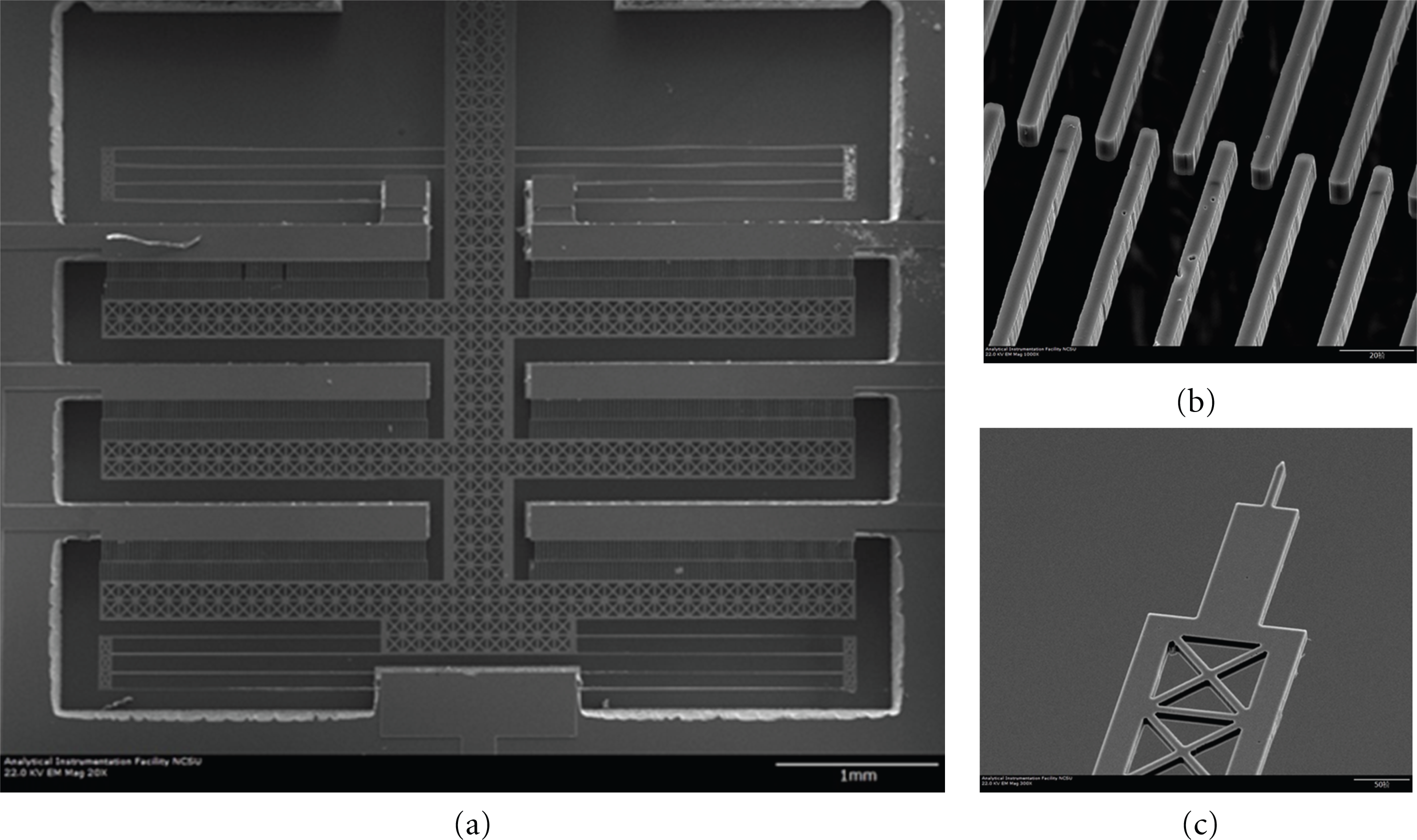
To characterize the static behavior of the fabricated single-axis stage, actuation voltages are given to the actuation comb drives, ranging from 0 V to 140 V with increment step of 10 V. The voltage is supplied by Keithley SourceMeter Model 2410. Output current is confined to less than 1 μA to prevent possible circuit shortage caused by transient spark. The motion is recorded and displacement is measured using a microscope with resolution of 1 μm. Figure 8 shows the measured displacement of the stage as a function of actuation voltage. At actuation voltage of 140 V, the stage gives a displacement of about 14 μm. The measured data fits quite well in a second-order curve as can be predicted by the theoretical analysis.

Static displacement characterization as a function of actuation voltage.
To assess the first natural frequency of the device, the dynamic behavior of the single-axis probing device is characterized. A sinusoid signal is generated by function generator (Agilent 33220A) and amplified by a voltage amplifier. This signal is then sent to a comb drive, and the amplitude of stage vibration is observed and optically recorded through the same microscope setup we used in the static test. A relatively wide-frequency-range sweep is initially performed to locate the device's natural frequency, followed by a fine sweep around the resonant frequency of the device. The vibration magnitude at different frequencies is plotted in Figure 9 as the frequency response. The measured natural frequency is approximately 1.5 kHz, while the predicted dominant natural frequency from FEA is about 1.38 kHz. The discrepancy may result from the dimensional variation from the fabrication process.

Magnitude of vibration around resonant frequency in air.
After the static and dynamic characterization of the device, the sensing combs are connected to a sensing circuit as shown in Figure 7. The capacitance change in the sensing comb drives is measured using Universal Capacitive Readout IC (MS3110) that is capable of sensing capacitance changes down to 4.0 aF/rtHz. The capacitance sensing resolution offers us a force sensing resolution of 2.8 nN with the total force measurement range about 60 μN. The schematic electrical connection is shown in Figure 7. The MC3110 is powered by a battery cell to minimize power-line noise. MS3110 is a differential capacitance sensor with limited measurement range. Since we only use one set of sensing comb to sense the capacitance, a tunable capacitor is used to balance the line capacitance for connecting the comb-drive to the sensor IC and zero out the sensor output, as shown in Figure 7. In typical laboratory environment, parasitic capacitance can be comparable to the capacitance from comb sensors. For example, a coaxial BNC cable usually introduces 1 pF/cm parasitic capacitance [20]. To balance parasitic capacitance from the connection, we manually adjust a capacitor trimmer so as to measure the net change of capacitance from comb sensors, which also helps to maintain the output voltage signal in proper range. In our experiment, the parameter of the capacitive IC is configured to have the output sensitivity as 6.75 volt/pF. The output voltage of the capacitive IC is recorded by a data acquisition system from National Instrument. Since an excitation signal of 100 kHz is generated within IC for capacitance measuring, an inductor is added in the actuation loop to reduce possible interference between actuation and sensing circuit loops. In our device design, the moving structure of the stage is the shared ground for both actuation and sensing structures and circuit. If the sensing circuit and actuation voltage is applied directly to the device, the high-frequency excitation sensing signal from the sensor IC can leak through the actuation loop, and bring large noise and measurement error. To isolate the sensing circuit and the actuation circuit, an inductor is connected in serial to the actuation comb-drive. For high-frequency sensing signal, the inductor has large impedance and block the signal/current leakage to the actuation loop. For the low-frequency actuation voltage, the inductor has very small impedance, which gives negligible voltage drop and do not change the actuation behavior. The inductor value is carefully selected to obtain good signal isolation from the sensing circuit, and on the other hand, to keep the actuation behavior unchanged.
Capacitance changes of comb sensor are recorded at each actuation voltage level from 0 V to 140 V. Figure 10(a) shows the measured capacitance change as a function of actuation voltage. The capacitance of comb sensor changes by 0.1 pF at actuation voltage of 140 V. The error bar in the plot indicates the variation introduced by noise during signal acquisition. This capacitance-voltage plot joint with the displacement-voltage plot from Figure 8 shows the relationship between the capacitance change of comb sensor and the displacement of stage. As shown in Figure 10(b), the linear regression function gives us a measured sensitivity of 6 fF/μm, which agrees quite well with theoretical value of 6.2 fF/μm. The small discrepancy can be attributed to dimensional deviations between the designed and the fabricated structure by the fabrication imperfections. This change in dimension affects the stiffness of the device and the capacitance sensitivity of the sensing comb drives.
Measured capacitance change of the sensing comb drives. (a) Capacitance change at different actuation voltage; (b) capacitance change as function of displacement of the stage.
6. Conclusion and Discussion
In this paper, an electrostatically actuated single-axis active probe was designed and fabricated. The probe as a functional manipulator is driven electrostatically by one set of linear comb drives. Other two sets of comb drives are used as capacitive sensors to sense the displacement and external force. The sensing comb structures provide capability of potential force-balanced sensing and closed loop control of the fabricated device. The designed device is fabricated on a 15 mm × 15 mm SOI die. The surface micromachining and deep reactive ion etching (DRIE) process are implemented in device fabrication. The fabricated device provides a displacement range of 14 μm at actuation voltage of 140 V. The measured natural frequency of the stage is 1.5 kHz. We obtain a sensitivity of 6 fF/μm which fits very well with theoretical value of 6.2 fF/μm for the ideal condition. The proposed single-axis probe is aimed at sensing cellular force which ranges from a few nN to μN and cell manipulation applications. In future work, the device will be tested with biological-like samples, like soft gel which has similar mechanical properties as cells. Moreover, by upgrading to higher-resolution capacitance sensing chip, we expect to achieve a higher force resolution.
Footnotes
Acknowledgment
This material is based upon work supported by the National Science Foundation through Grant Award no. CMMI 0800863.