
Abstract
Abstract
The past decade has seen revolutionary advances in three-dimensional (3D) printing and additive manufacturing. However, a technique to create 3D material microstructures of arbitrary complexity has not yet been developed. We present the conceptual design of a 3D material microprinter as a concrete step toward an eventual 3D material nanoprinter. Such a device would enable the use of heterogeneous starting materials with printing resolution on the order of tens of nanometers. By combining a pick-and-place particle transfer method with a custom-built laser sintering optical microscope, the core components of the 3D printer are once again reimagined. This advance moves toward generalized material synthesis as an experimental technique to complement computational materials discovery of materials with unique structures and high interface density, such as 3D nanocomposites, metamaterials, and photonic structures.
Introduction
I
The current absence of a 3D nanoprinter represents a major obstacle to the rapid realization of many materials developed by computational materials discovery (CMD), 3 an emerging area of materials science research. Presently, CMD is in a unique position where the size of atomistic models has not yet converged with the typical feature sizes that are feasible to fabricate. CMD allows the design and simulation of material properties that do not exist naturally, from the atomic scale to the mesoscale and the macroscale. 4 This has led to the design of new alloys, 5 superconductors, 6 and surprising phases of common compounds, 7 some of which have been experimentally synthesized. However, no universal method exists to bring CMD-designed materials into reality. Instead, they are built one at a time, with custom techniques and starting materials tailored to each end product.
In the past, the ability to synthesize material microstructures using Edisonian-based methods outpaced the slower, or previously nonexistent, abilities to simulate materials on the computer. This balance has completely reversed in the past 10–15 years, with the ability of CMD vastly outpacing the ability to bring CMD-simulated microstructures into reality. Notable examples include the prediction of an insulating, transparent phase of sodium 7 and designer nanoparticles with optimized surface properties. 8 Now the race is on to physically recreate materials predicted by CMD. Of particular interest to fields such as radiation materials science are nanocomposites, as the combination of materials with a high interface density both blends the macroscale properties of the constituent phases and provides the ability to remove atomic-scale radiation damage as it is produced. 9 Notable examples include Nb-Cu nanolayered composites designed by Demkowicz et al. 10 that were produced using accumulated roll bonding. While such work is inherently limited to 1D nanocomposites, increasing the interfacial density by moving to 3D could further enhance radiation resistance by eliminating or slowing microstructural evolution due to layer coarsening. 11
Similarly, the flurry of research into 2D crystals, such as graphene and MoS2, promises the possibility to combine different 2D crystals that are exfoliated from their bulks and then layered into a new van der Waals (vdW)–bonded artificial 3D heterostructure. The resultant 3D crystals are readily designed by ab initio atomistic models, but the practical process of layering the 2D crystals is difficult to master and painstakingly slow. 12 It is crucial that this process is automated, and a pick-and-place printing technology seems to be a clear solution.
The field of metamaterials, or superstructures whose properties behave differently from their smaller constituents, has led to the creation of entirely new materials, such as terahertz magnetic antenna arrays, 13 and negative refraction-index “cloaking devices. 14 ” Many other desirable properties can be tuned via metamaterial creation, as was recently summarized by Garcia et al. 15 As increasingly complex structures are designed and simulated, our ability to fabricate these structures quickly loses pace with the CMD aspect of metamaterial design. Were a way to quickly assemble superstructures of heterogeneous building blocks to exist, then the only physical bottleneck would be the ability to synthesize the building blocks themselves, not their optically/electrically/magnetically active superstructure.
In this article, the existing methods of 3D printing are first reviewed as they apply toward satisfying this missing material synthesis need. Next, a new type of 3D printer is proposed, which satisfies all the requirements of a 3D material nanoprinter. Realizations of specific components are then demonstrated, while existing obstacles to the realization of other components are delineated. Finally, the potential impact that a 3D material nanoprinter would have on the field of CMD with physical synthesis is discussed.
Background: Existing Methods of 3D Printing
The field of 3D printing continues to make leaps and bounds, with successive implementations pushing the frontiers of resolution and widening the diversity of printing media. While initially working with starches and polymers, 3D printing technology has expanded to incorporate metals, 16 sintered ceramics by extrusion, 17 selective laser sintering, 18 and a number of other materials. Modern devices, such as the Stratasys Dimension Elite, reach resolutions of 250 μm, 19 while those that use stereolithography rather than fused media reach into the hundreds of microns, recently achieving layers that are only tens of microns thick. 20 Two photon polymerization techniques can achieve some of the best resolutions available at present, with 200 nm repeatable features achievable. 21 However, such techniques are fundamentally limited by effects of surface tension of the fusing medium, an ability to remove heat from the sintering volume, or the quality of the optical mask for stereolithography. In addition, all the above methods have the fundamental limitation of homogeneous media, meaning that one type of material and composition must be the medium for construction.
Not all 3D printing methods are additive in nature. Subtractive methods have shown more promise at increasing resolution of 3D printing. Recent advances in two-photon lithography have produced wafer-sized 3D periodic structures with micron resolution. 22 Ion beam lithography, by avoiding photons entirely, can extend the resolution below the 100 nm range. 23 The structures formed can be heterogeneous if layers of different compositions are deposited in sequence before lithographic steps. A combination of holographic lithography and two-photon laser writing has been demonstrated to create 3D photonic crystals by selective creation of localized structural defects. 24 Here the throughput is greatly enhanced by using holographic lithography to determine an overall structure, and two-photon writing to make smaller, localized modifications. Soft lithography, meanwhile, has been used to create 3D, multilayer microfluidic devices, 25 while a similar method combined with a 3D sugar printer is used to create sugar-filled channels that can be dissolved after fabrication to create microfluidic channels. 26 Most recently, IBM has developed a scanning probe lithography system, which can exceed the electron beam lithography resolution limit, 27 subtractively creating 3D replicas of objects with single nanometer height resolution. Subtractive methods, however, cannot create 3D structures of arbitrary complexity with respect to both shape and material heterogeneity.
Additional modern 3D printer improvements include printing in liquid metal droplets, 28 submicron photolithography for material removal in cellulose and other media, 29 3D printing of nanowalls made from electrospun nanofibers, 30 and 3D holographic lithography for near-instantaneous nanostructure fabrication in soft materials. 31 Weld-based additive manufacturing by gas metal arc welding, 32 powder bed sintering, 33 and electron beam free-form deposition 34 can produce heterogeneous structures if different filler metals, powder layers, or carrier gases are used, respectively. However, many of these techniques require large amounts of energy deposition, limiting their resolution. 35 Meanwhile, potential exists for the targeted positioning of much smaller, possibly heterogeneous structures onto substrates. The efficacy of this approach has been demonstrated in previous research, where an atomic force microscopy (AFM) was used to arrange silicon nanoparticles on a silicon substrate. 36 In addition, IBM recently revealed its movie, A Boy and His Atom, consisting entirely of stop-motion freeze-frames of single atoms arranged on a flat substrate, 37 demonstrating the ultimate resolution attainable by precise arrangement of single atoms.
These studies and achievements demonstrate the feasibility of atomistic surface position control with high accuracy and repeatability. However, none definitively enable the direct creation of proposed materials, such as some of the aforementioned vdW heterostructures, metamaterials, and 3D nanocomposites. 3D printing these materials would require the ability to pick and place the fundamental building blocks of the metamaterial, and to fix them into position for device creation. These blocks would have to be made by some other method, such as e-beam lithography or self-assembly. Due to the expense of fabricating the starting particles, a successful 3D material nanoprinter should use them efficiently and generate minimal waste.
The current status of 3D printing in support of the goal of true 3D, heterogeneous, multimedia, nanoscale printing is summarized in Table 1. Here, only additive methods are considered for reasons stated above. Required features of a 3D material nanoprinter include the following:
• True material heterogeneity, meaning that arbitrary numbers of arbitrary starting materials could be used to fabricate a superstructure
• Nanoscale resolution, where the manipulatable size of the starting materials must be equal to or smaller than the smallest feature of interest in the material microstructure
• Ability to utilize prefabricated building blocks, so that metamaterials consisting of building blocks with unique structures can be directly assembled into superstructures
• Low-energy deposition, so that the 3D printing process does not melt or alter the crystal phase of the starting materials
In addition, the following features would be beneficial, though not required:
• Low waste, so that potentially expensive or hard-to-manufacture building blocks are not discarded • High throughput, so that fabricability can keep pace with the speed of CMD
As can be seen in Table 1, no currently existing technology simultaneously meets the requirements of nanoscale resolution, high heterogeneity, and low enough energy deposition. Next, we propose a method that may meet these needs, based on picking and placing microparticles (now) and nanoparticles (in the future) into position, using a low-power laser to sinter the particles to their new nearest neighbors, and repeating until the object is completed.
Methods: 3D Microprinter Design
We have designed and nearly completed building the first prototype of our 3D micromaterial printer, shown schematically in Figure 1. The printer functions at the one-micron resolution level, close to the limit of optical microscopy. It consists of a custom-designed optical microscope, with a 400 mW ultraviolet sintering diode laser in focus with the microscope's optical plane, and a Sutter Instruments nanomanipulator with 40 nm resolution to pick-and-place starting materials from an “artist's palette” of non-close-packed microspheres. In our system, an x–y stage positions the substrate (and eventually the object under construction) beneath the optical/laser focal spot, while a piezo-actuated z-stage with ∼100 nm resolution moves the object into focus. Then, the nanomanipulator picks up a particle from the palette of starting materials using a sharp tip, such as that from a scanning tunneling microscope. Next, electrostatic attraction, vdW forces, or other passive methods cause adhesion to the tip, which transports the particle to the focal point of the microscope. Finally a laser pulse sinters the particle into place. A schematic of the particle pick-and-placement procedure is shown in Figure 2.
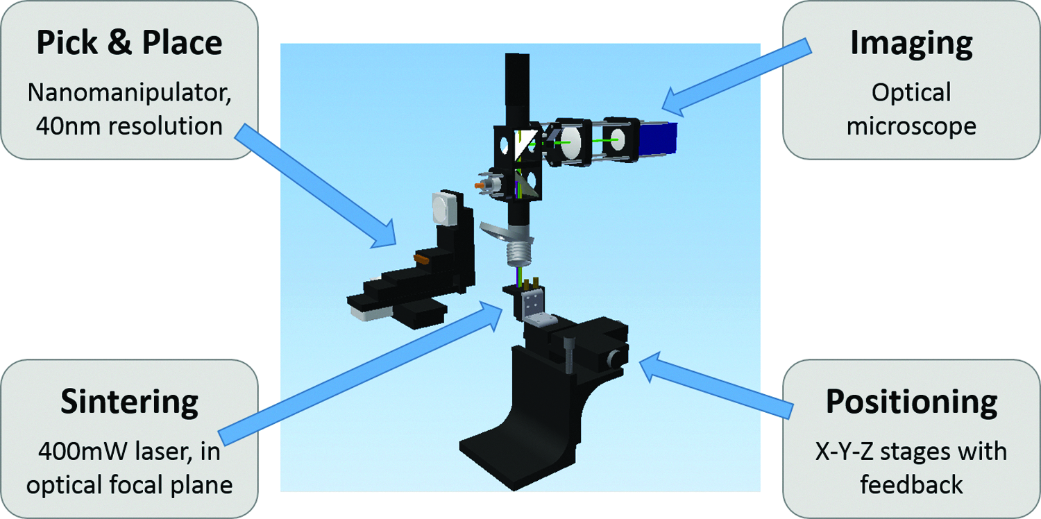
Conceptual schematic of the pick-and-place 3D microprinter. Color images available online at www.liebertpub.com/3dp
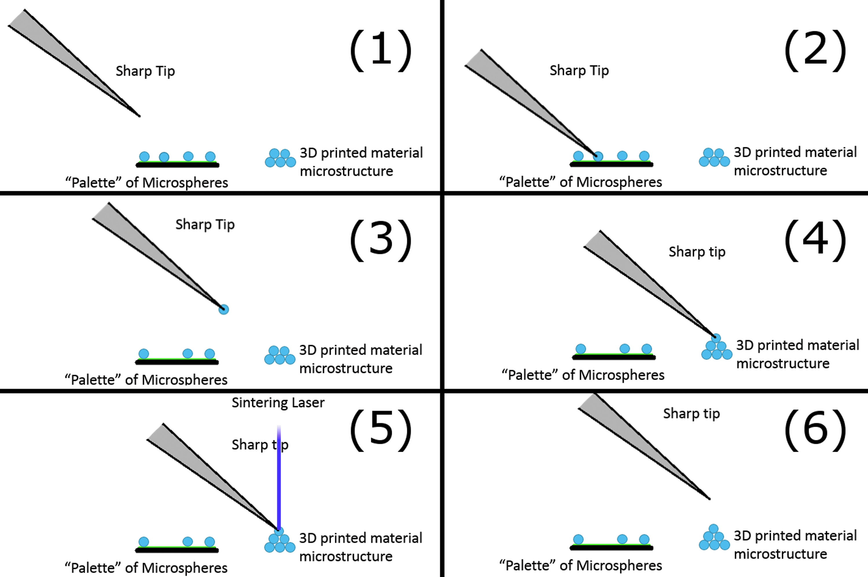
Schematic of the pick-and-place procedure for particle deposition. A sharp tip
By sintering the particle into place, the system can overcome vdW attractive forces (which increase with decreasing particle size) that retain the particle on the nanomanipulator during the transport step. Of critical importance is sintering the particle into place without considerable melting, so as not to substantially change the crystal structure of the created material. Additionally, sintering enables the use of building blocks smaller than the wavelength limitations of the laser light, since already-sintered blocks within the heated area will be only minimally affected.
A number of challenges exist to realization of this 3D material nanoprinter, including demonstration of the following:
1. Construction and demonstration of controlled, patterned particle sintering using the X–Y–Z stage to move the object into the microscope/laser focal spot 2. Creation of the “artist's palette” of non-close-packed, uniformly dispersed starting particles 3. Demonstration of the pick-and-place method of particle retrieval and deposition 4. Cross-material sintering studies, to map out the design space of fabricable, heterogeneous materials, and associated laser pulse power/shape 5. Characterization of the final printed materials, especially in terms of porosity and microstructural uniformity of the smallest building blocks
Results: Component Realization
Of the major components of the proposed 3D material printer, the first two have been built and demonstrated: the sintering, patterning optical microscope, and the non-close-packed lattice of starting particles. Here the details of these first two components are described, along with demonstrations of their capabilities.
Sintering, patterning optical microscope
Figure 3 shows detailed photos and a schematic of the combined optical microscope and sintering laser, with an onboard camera to allow for in-operando images and movies to be taken. Of critical importance to this optical incarnation of the 3D material printer is an infinity-corrected objective lens with minimal chromatic aberration, to ensure that the laser and white light LED illumination are focused to the same spot. The laser can enter the microscope either through an optical fiber or in free space. A radio frequency signal generator is used to modulate laser power, duty cycle, and waveform. The focal point of the microscope remains the same, while the stage and particles are moved into view.
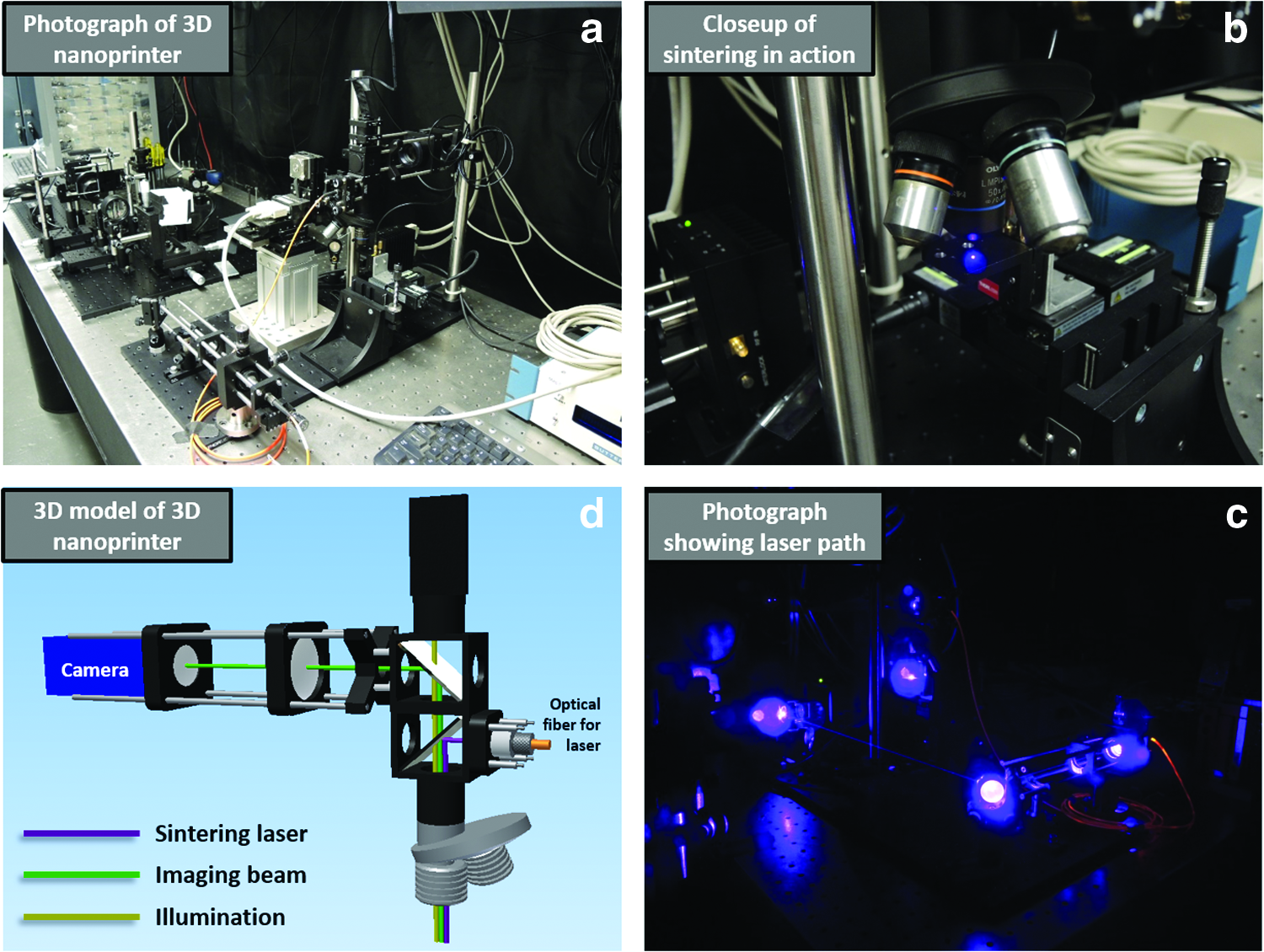
Photographs and a schematic of the 3D micromaterial printer. Clockwise, from top left:
Figure 4 demonstrates examples of micron-scale sintering patterns achieved on 2D media using this system. In the figure, a fiber-coupled multimode laser was able to achieve a four micron spot size on a close-packed layer of 1 μm polystyrene spheres, enough to ensure coverage of the single micron particles without too much energy deposition to the surrounding materials. It is clear that the center of the laser spot was too high in power, and completely sintered or even ablated the particles. Detailed interparticle sintering studies, currently underway, will determine the optical laser pulse length, amplitude, and waveform for each pair of starting materials.
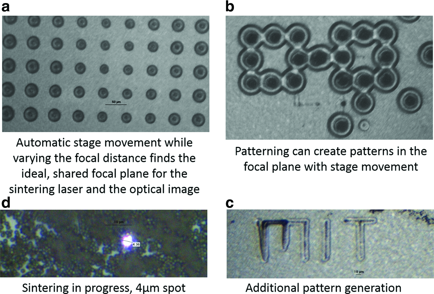
Demonstrations of the sintering–patterning system using X–Y–Z stage movement. Clockwise, from top left:
Non-close-packed starting material lattices
The ability to deterministically retrieve single particles in an automated fashion represents a rate-limiting step in the throughput and functionality of a 3D material printer. Therefore, a palette of non-close-packed, regularly spaced starting materials would allow for automatic, high-speed retrieval. Much work has been demonstrated in creating close-packed arrays of particles, such as using a Langmuir–Blodgett trough 39 or spin coating. 40 Techniques to create non-close-packed structures have included reactive ion etching of close-packed particles, 41 creating a non-close-packed mask using close-packed particles from spin coating, 42 and stretching a soft substrate. 43 Methods that directly create non-close-packed clusters of particles have been shown, using a film of liquid crystals as the substrate. 44 However, methods to rapidly self-assemble large (square inch) arrays of particles regularly separated by many particle diameters are scarce.
We have developed a new method to create square-inch-sized regular lattices of polystyrene microspheres in support of this goal. The technique relies on the deposition of mist particles containing single microspheres onto a liquid interface, whereby they self-assemble into regular arrays via a combination of attractive and repulsive forces. Figure 5 shows images of colloidal lattices of 1 μm ± 2% polystyrene microspheres, sourced from Alfa Aesar in Massachusetts as-deposited and after 12 h exposure to air. Medium range order is observed, as evidenced by the Lennard–Jones-type radial distribution function (RDF), shown in Figure 5, which analyzes the likelihood of finding one particle at a certain distance from another. The RDF shows that up to five lattice spacings, ordered particles still exist. It is evident in Figure 5 that defects still exist in the colloidal lattice. Longer range order may be achievable by defect concentration reduction.
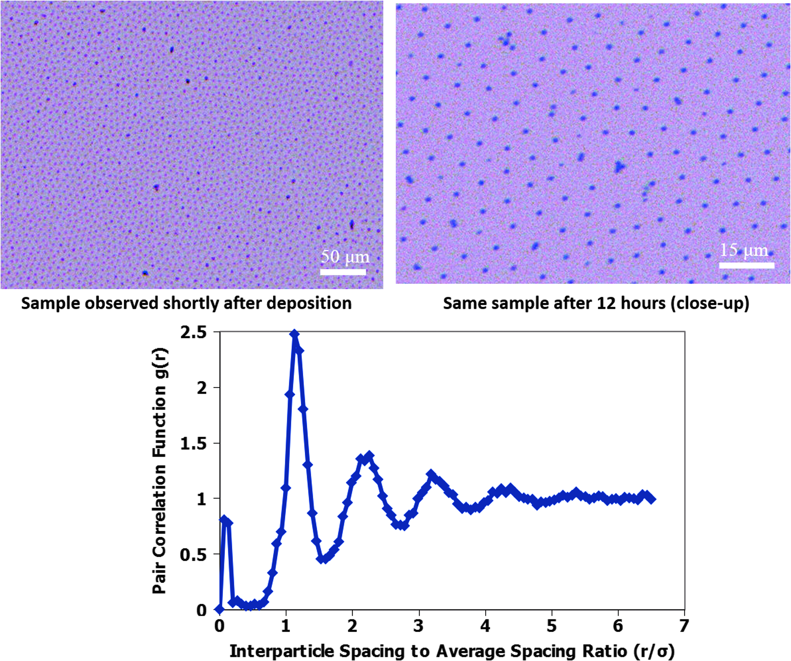
Colloidal lattices created using the new mist-particle deposition method. (Left) Large-scale image of the colloidal lattice on a water–air interface. (Right) Image showing stability of the lattice after 12 h exposure to air. (Bottom) Radial distribution function from a section of the image in Figure 5, exhibiting medium range order. Color images available online at www.liebertpub.com/3dp
Next steps
Now that semiregular lattices of polystyrene particles can be reliably grown, work is underway to reduce the defect density and improve lattice regularity of the starting particles, as well as to apply the deposition process to other microsphere materials. This will be tested by successive lattice creation and analysis by the RDF, as shown in Figure 5. The more oscillations this function possesses, and the narrower they are, the more regular the lattice is. Then the pick-and-place method can be attempted with automatic particle retrieval, followed directly by the printing of the first micron-scale heterogeneous material microstructure.
Following demonstration of the 3D material microprinter, the entire system design will be rebuilt for installation into a large chambered scanning electron microscope (SEM), so that observation of the pick-and-place methods and particle attachment may proceed in situ at the nanoscale. This will require utilization of the SEM positioning stages, a higher-resolution positioning system (such as the existing Omniprobes for focused ion beam instruments), and the recreation of the starting particle palette with a far smaller particle size and spacing.
One major challenge specific to metamaterials may be the ability to pick and place building blocks without rotation about any axis. This is because some metamaterials rely on an ordered structure of oriented substructures, whereby misorientation of a single particle may degrade the metamaterial's properties. This issue will be addressed only once a functioning 3D nanoprinter is complete.
Discussion: Potential for Applicability and Impact
The successful demonstration of nanoscale 3D printing will profoundly impact industrial and academic research, providing a low-cost technique to construct nanoscale devices, and therefore opening up the possibility of nanofabrication to new groups across the globe. More generally, it is also expected that this technology will impact the way in which nanoscale rapid prototyping is performed—we expect that new design methodologies will arise from the 3D nanoscale printing technology. Based on our present findings, the low printing speed of about seven particles per minute would exclude the direct application of this technology to macroscale devices, but the flexibility afforded by the technique will be relevant for advanced materials research and fabrication of microscale devices. In particular, the fields of metamaterials and structural materials for low-carbon energy will greatly benefit from the ability to rapidly prototype novel micro- and metastructures, fostering creativity across fields of materials science and engineering.
The ability to achieve correspondence between simulations and syntheses of newly designed materials is of particular interest and usefulness. For example, much of the reason for the slow development of new structural materials for nuclear applications stems from the difficulties of achieving direct correspondence between models of radiation damage and irradiation experiments. This is due to the inability to create the same initial conditions on the computer and in the laboratory. Computers ideally utilize regular, periodic structures for faster simulation, while laboratory syntheses possess real imperfections and tolerances. An illustrative example could be the simulation and measurement of the defect sinking strength of carbides in a simple steel. A fast atomistic simulation would study the accumulation of defect clusters near a unit cell containing a single carbide particle, with periodic boundary conditions. Meanwhile, the fabrication of a real steel would create a distribution of carbide particle sizes and spacings, leaving the scientist to try to map the results of the simulations to a real experiment. A more realistic simulation requires a far larger volume of atoms to capture a representative carbide size and spacing distribution, which usually places it outside the realm of accessible computing power. Were a 3D material nanoprinter to exist, it could simply print a lattice of similarly sized carbide particles in an iron matrix, increasing the validity of a smaller simulation with periodic boundary conditions, and enabling theory and experiment to progress as new relations are discovered.
In addition, a number of proposed metamaterials have not yet been fabricated, often due to requirements of orientation, chirality, or magnetic alignment in order to fulfill their functions. Examples include chiral split ring infrared resonators, 45 broadband negative refraction index materials, 46 and electromagnetically induced transparent structures, 47 which are presented with numerical simulations instead of direct fabrication. An ideal example is that of Kim and Gopinath, 48 who propose a 3D, cubic lattice of high-dielectric resonators embedded in a low-dielectric matrix. This is quite analogous to the design of a computationally ideal steel, with a 3D, cubic lattice of carbides embedded in a matrix of iron. In situations like this, the proposed pick-and-place printer could be used for multiscale fabrication. An array of machines can construct the unit cell building blocks, such as the single cubic resonators, which can be used as the starting palette in a larger pick-and-place printer. The printing time of this method in continuous production is shorter than that of a single machine by a factor of (N – 1), where N is the total number of printers. For the example of the above cubic lattice metamaterial, a single cube may be composed of 27 starting particles (3 ×3 × 3 cube). Starting with 1 μm particles and 11 printers, a 100 × 100 × 10 μm superstructure could be built in about one day given the presently observed unoptimized printing speed. In this way, the proposed new type of 3D printer could speed the pace of multiscale CMD, by enabling the direct, multiscale fabrication of proposed hierarchical metamaterials.
Conclusions
A new type of 3D printer capable of directly creating materials is proposed, along with a new set of constraints necessary for success. Key components of a microscale version have been demonstrated in support of the eventual nanoscale device. Work is underway to complete the microscale version, which will subsequently be rebuilt inside an SEM to create a true 3D material nanoprinter. The ability to print material microstructures would bring the speed of rapid material synthesis back in line with the new, fast-paced paradigm of CMD, enabling direct material development and hastening the ability to test correspondence between simulations and syntheses of novel materials.
Footnotes
Acknowledgments
The authors are grateful to the MIT International Design Center for funding the research described herein. The authors also acknowledge useful conversations with Skylar Tibbits about the applicability of the proposed 3D printer.
Author Disclosure Statement
No competing financial interests exist in the funding of this work.