
Abstract
In polycrystalline piezoelectric ceramics, ferroelectric domain texture is the most important parameter influencing the attainable electromechanical performance. High piezoelectric properties are obtained when the maximum poling of the material is achieved. This condition can be favoured by modifying material composition, poling routes or by proper grain texturing. Hence, it is necessary to characterise domain texture, in order to develop piezoceramics with improved performance. In this review, an outline of the methods for ferroelectric domain texture determination will be given, with focus on microscopic techniques. The advantages and complementarity of methods like X-ray and neutron diffraction, electron diffraction, and Raman spectroscopy will be highlighted.
Keywords
Introduction
Modern piezoelectric devices such as sensors/actuators or motors are largely based on piezoceramics. 1 These materials are by the vast majority ferroelectric, i.e., they possess spontaneous polarisation if cooled below the Curie temperature, Tc, and this polarisation can be oriented by applying a sufficiently high electric field (a process known as poling). The newly achieved polarisation is preferentially oriented along the applied field direction, and persists to a large extent (the so-called remanent state) after field removal, i.e., it is permanent. After poling the material displays macroscopic piezoelectric behaviour. 1
Piezoelectric materials are often found in devices in their polycrystalline form, mainly due to the ease of production. These materials can possess very high electromechanical coupling and piezoelectric coefficients, which makes them suitable for actuator applications. Piezoelectric actuators are widespread in the automotive industry as fuel injection systems 2 (as multilayers), gyroscopes, 3 positioning devices 4 or micro-electromechanical systems.5,6 The performance of those materials in terms of field-induced elongation (strain) depends on the switching of ferroelectric domains, or in other words the movement of domain walls (DWs).7-14 Both 180° and non-180° DW motion are intended as extrinsic (i.e., as opposed to intrinsic lattice strain) contribution to the piezoelectric effect, 8 whereby the latter may be the largest contribution to the macroscopic lattice strain. 15 17 Extrinsic DW movement is enhanced if the lattice aspect ratio is reduced, since the decrease in lattice tetragonality leads to decreased intergranular constraints. 17 This is at the basis of the high electromechanical coupling obtained at the morphotropic phase boundary (MPB) of many ferroelectric solid solutions.17,18 In fact, it has been demonstrated 17 that non-180° DW motion constitutes the majority of the electromechanical strain response of certain materials, and that the relative contribution to the overall strain increases with tetragonality. A non-negligible contribution, however, is due to electric-field induced 180° DW movement in non-polar crystal directions. 17 In polycrystalline ceramics only a domain orientation distribution can be defined, since the movement of domains is constrained to the degrees of freedom allowed by the underlying ‘native’ grain orientation. Therefore, upon poling, domains will never be 100% oriented in the field direction, but will assume the best-possible orientation distribution. 19 The maximum achievable domain orientation distribution depends on crystal symmetry and on the grain orientation distribution. Jones et al. 20 22 calculated such saturated distribution functions and concluded that a monoclinic symmetry allowing polarisation rotation possesses the maximum achievable domain fraction, in accordance with the high electromechanical coupling measured in those symmetries (i.e., at the MPB of lead zirconate titanate 23 25 ). These considerations are in principle valid for any composition or material. The choice of different compositions, solid state mixtures or processing routes, however, allows tuning the electromechanical properties of the piezoceramic by reducing the tetragonality,17,26 inducing a monoclinic phase or a mixture of phases,14,27, 28 or by modifying the grain orientation in order to allow for higher domain orientation in the direction of poling.29,30 This latter aspect can be achieved by texturing the ceramic by templated grain growth (tape casting), 31 and it proved very efficient to increase DW movement in lead-free ferroelectrics. 32
Clearly, the analysis of domain orientation distribution is a key factor in the development of piezoceramic devices. Being able to describe domain orientation changes in dependence of composition, electric field and mechanical stress not only allows selecting the best materials and compositions for a definite application, but also improving the performance and the stability of the device in service. This review presents various methods for the analysis of domain orientation distribution (texture) in piezoceramics, focussing mainly on microscopic techniques. After a short overview on macroscopic methods, we will describe texture determination by diffraction techniques (X-ray, neutron diffraction and electron backscattered diffraction – EBSD). Subsequently, in chapter 4, we will present the use of Raman spectroscopy, and lastly (in chapter 5) we will briefly compare all methods and mention the possibilities offered also by other techniques. Models of texture representation were already discussed in many excellent reviews33-36 and thus will not be detailed here. Rather, we will recall the main concepts whenever necessary. Some definitions, however, ought to be given beforehand:
The Orientation Distribution Function (ODF) is defined as a multiple of a random distribution (MRD), f(g), i.e., the density of domains oriented in a certain direction g with respect to the density of domains in a randomly oriented material, with g given by Euler angles (ϕ, θ, ψ). The ODF can be represented as discretised
37
or through analytical functions, such as spherical harmonics.
15
More details will be given in the following sections. Pole figures show the densities of a given crystallographic direction along all sample orientation directions.15,21 Inverse pole figures represent the densities of all crystallographic directions along a given sample direction.15,21
Macroscopic texture determination
Historically, the most common method to reveal ferroelectric domain orientation in ferroelectric ceramics was etching, i.e., exploiting the differential etching speed of the different crystallographic directions.1,38, 39 This method, however, is capable of detecting only out-of-plane domain contrast. Moreover, quantitative texture determination is not possible and only qualitative comparisons can be carried out applying image analysis techniques.
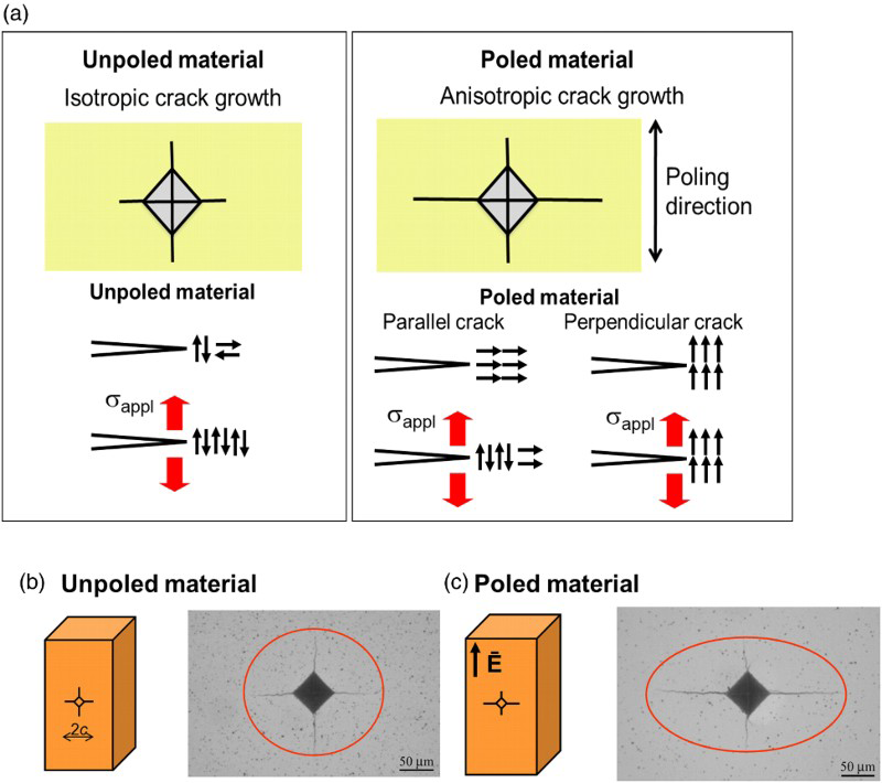
A more convenient method to quickly determine the effects of preferential domain orientation (i.e., the macroscopic texture degree) is the use of Vickers indentations and the measurement of the induced crack lengths with respect to sample or poling axes.40-43 In fact, the tensile stress at the crack tip induces domain switching by means of the ferroelastic effect:44,45 Domains tend to align themselves perpendicular to the crack propagation direction. This process consumes the available elastic energy and thus increases the activation energy barrier for the formation of new crack surfaces.
43
As a consequence, toughening effects occur, which can be summarised in two extreme cases:
Random domain orientation (e.g., unpoled material): Cracks propagating in any direction will always encounter the same domain distribution. Domain switching occurs always in the same amount, and accordingly the toughening effect is the same and the cracks have all the same length in every direction. Preferential domain orientation (e.g., poled material): Cracks propagating parallel to poling will produce non-180° domain switching, whereas cracks perpendicular to poling will not induce any switching, since the domains are already perpendicular to the crack propagation direction. As a consequence, cracks parallel to poling will be shorter than the cracks in the unpoled material, whereas cracks perpendicular to poling will be longer than in the unpoled case.
These effects are displayed in Fig. 1a. Figure 1b and 1c report micrographs of Vickers indentations placed on the polished surface of unpoled and poled lead zirconate titanate (PZT) bulks. Cracks in the poled material are anisotropic and longer/shorter with respect to the unpoled sample (in the direction perpendicular/parallel to poling, respectively). The crack growth resistance (CGR) is a measure of the material's toughness and can be expressed by the following equation:
46
a Schematic showing ferroelastic domain switching at the tip of Vickers indentation cracks. b and c Micrographs of Vickers indentations on the surface of unpoled and poled PZT bulks, respectively
Characterisation of texture by diffraction
X-ray and neutron diffraction
Diffraction by X-rays or neutrons is probably the most popular method to analyse ferroelectric domain texture in piezoceramics, with first reports dating back to 1957.12,13,48-50 Diffraction methods used for this purpose can be divided into three categories: (i) Laboratory X-ray diffraction (XRD), (ii) synchrotron XRD and (iii) neutron diffraction. Due to its compact size, the former method is readily available in many research institutions, however the relatively low achievable X-ray energy allows only surface-sensitive measurements.
20
To this respect, synchrotron sources easily provide transmission measurements, which enable greater sampling volume and thus detection of the overall texture of the material.
20
The same applies to neutron diffraction, since neutrons can penetrate into certain materials further than laboratory X-rays.
15
Obviously, neutron and synchrotron X-ray sources can be obtained only in few facilities around the globe, for which access is limited by the acceptation of experimental proposals. The advantage of those measurements, however, should not be underestimated. Modern synchrotron and neutron sources provide unique capability of carrying out in-situ measurements by applying concurrently electric field and mechanical load,
51
which is hardly realisable in a laboratory XRD equipment. Moreover, although area detectors have been implemented recently also in laboratory XRD,
15
the measurement still requires sample rotation in order to distinguish texture along different sample directions. This is not needed in synchrotron XRD or neutron diffraction measurements. An example of a transmission synchrotron XRD diffraction setup using an area detector is given in Fig. 2a.
18
a Experimental setup for transmission synchrotron XRD with area detector. The 2D diffraction image shows Debye-Scherrer rings which are then binned and integrated in order to obtain the 2θ diffraction patterns in function of the angle to the E-field as shown in the graph on the left. Reprinted with permission from Ref.
18
b Diffraction spectra near the (002) and (200) reflections close to the poling axis of a tetragonal PZT; the upper spectrum is from neutron diffraction experiments and reports a Rietveld refinement (solid line), the one below from XRD (showing peak fitting). Reprinted with permission from Ref.
15
c (002) pole density distributions (ODF) of tetragonal PZT as a function of poling electric field. The saturated theoretical domain distribution is also shown. Reprinted with permission from Ref.
21
d 90° domain switching contribution in function of composition for BCT-BZT. Reprinted with permission from Ref.
17
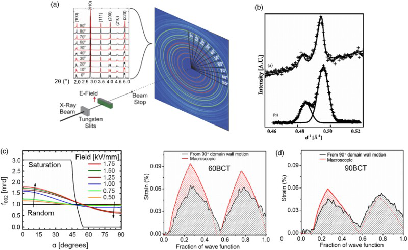
Both XRD and neutron-based techniques display as a result the same diffraction pattern, although some differences in peak resolution may occur (also between different neutron sources), as mentioned by Jones et al.
21
As evident from Fig. 2a, using an area detector the results consist of Debye-Scherrer rings that can be integrated in selected slices (bins) at different angles with respect to a relevant sample direction (e.g., the poling axis, or the axis of applied electric field or mechanical stress).
18
After the integration procedure, traditional (2θ) diffraction patterns are obtained in dependence of the aforementioned angles (cf. Fig. 2b showing the tetragonal [002] and [200] reflections). In polycrystals, the integrated intensity of a reflection peak is directly related to the number of crystallites in which the reflection is aligned with the direction of scattering. Thus, the integration of the obtained Debye-Scherrer rings along different angles directly gives information, for each crystal variant, on the amount of crystallites oriented in the sample orientation space.15,18 In other words, the whole ODF can be obtained by one simple measurement, and is generally given as a MRD, with respect to the non-oriented state. In the case of a tetragonal perovskite crystal, the volume fraction of domains with the c-axis aligned with a certain sample direction (e.g., angle to the poling direction) is15,18,
52
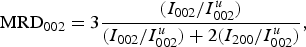
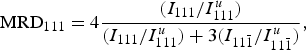
 planes, whereas the factor of 4 refers to the domain variants in the rhombohedral structure. Note that the MRDhkl values always refer to changes in crystal orientation (i.e., not of the crystal electric dipole) and thus can be used only to detect non-180° domain switching. This allows determining the contribution of non-180° domain switching to the overall electromechanical response.17,20,
21
In addition, by monitoring the shift of the 111 reflection peak it was demonstrated,18,53 that in tetragonal polycrystals a huge contribution to the electromechanical response is given by lattice strain in non-polar directions. This has been ascribed to dynamic strain accommodation due to intergranular interactions upon domain switching.
18
planes, whereas the factor of 4 refers to the domain variants in the rhombohedral structure. Note that the MRDhkl values always refer to changes in crystal orientation (i.e., not of the crystal electric dipole) and thus can be used only to detect non-180° domain switching. This allows determining the contribution of non-180° domain switching to the overall electromechanical response.17,20,
21
In addition, by monitoring the shift of the 111 reflection peak it was demonstrated,18,53 that in tetragonal polycrystals a huge contribution to the electromechanical response is given by lattice strain in non-polar directions. This has been ascribed to dynamic strain accommodation due to intergranular interactions upon domain switching.
18
One notable example of application of this technique is the study Jones et al. performed 22 nearby the tips of cracks stabilised in a compact tension (CT) experiment. By spatially resolved analysing the diffraction patterns in an area 2 × 2 mm2 wide (beam size 50 × 50 µm2) they determined that [002] domains preferably orient themselves perpendicular to the crack propagation direction. More precisely, the domains tend to follow the deviatoric stress contour. In their work, they also determined the extent of lattice strain from XRD measurements, and the amount of remanently oriented domains in the crack wake upon crack advancement. A later experiment 54 showed also the mechanical depoling effect around a crack loaded in the CT configuration.
Synchrotron XRD has been used recently also to determine the contribution of non-180° domain switching to the overall electromechanical response in lead-free piezoceramics. This field of study is of the highest importance given the need for replacing PZT with valid lead-free alternatives. In their contribution, Tutuncu et al. 17 investigated a Ca- and Zr-codoped barium titanate composition (BCT-BZT) under in situ application of bipolar electric field cycles. Various compositions were tested, and they were able to determine that a stronger degree of domain alignment is attainable in materials with lower tetragonality. In particular, rhombohedral compositions showed increased electromechanical response, but the extent of lattice strain contributions was higher than tetragonal compositions, where almost all elongation can be ascribed to non-180° DW motion (cf. Fig. 2d for rhombohedral and tetragonal BCT-BZT – 60BCT and 90BCT, respectively).
Other notable contributions are, among others, the recent paper by Daniel et al., 51 in which XRD was used to study lattice anisotropy during blocking force measurements in PZT (although only strain and not texture was quantified), and the study by Pojprapai et al. 55 dealing with electrical fatigue. In this latter contribution, texture measurements were applied to link the reduction of piezoelectric performance upon increasing number of cycles with the domain pinning effect. The literature about texture measurements in piezoceramics by XRD and neutron diffraction is extremely broad. For deeper insight into this field of study, the reader is referred to the excellent reviews by Jones et al.20,21
It is worth discussing briefly data treatment methods. In principle two routes can be followed: Rietveld refinement or peak fitting. The Rietveld method is based on the modelling of the entire diffraction pattern under the consideration of crystal structure, instrument geometry and optics, lattice parameters, phase fraction, crystallographic texture and microstrains.56,57 This method thus requires knowledge of instrumental parameters, which are obtained by measuring standard samples. The refinement relies on a least-square fit of the whole diffraction pattern, and as such can be cumbersome. A valid alternative for quantitative analysis is the use of peak fitting. In this case, a portion of the pattern is singled out and fitted with spectroscopic profile functions, thus extracting peak position, intensity and width. These parameters can be then employed to calculate lattice strain or texture, for instance. 21 The principal limitation of peak fitting is the required knowledge of the exact number, position and type of peaks to be used as initial approximation for the fitting. This can be very difficult to determine for a material with mixed phases, and for this reason generally in PZT only pure rhombohedral or tetragonal samples have been investigated so far. A possible way to address this issue is first performing a Rietveld refinement on a powdered sample in order to obtain the phase fractions, and then applying constrained fitting on the area of interest of the diffraction pattern.
Electron backscattered diffraction
EBSD emerged recently as an interesting method for the visualisation of domain structures in ferroelectric materials.33,58 At the basis of the attempts by many researchers is the fact that EBSD has the potential to detect domain orientation in spatially resolved fashion and with sub-µm spatial resolution. 33 The method is based on the diffraction of a collimated electron beam from lattice planes, and thus it is realised in a field-emission scanning electron microscope, which reaches the high acceleration voltage (up to 20 kV) necessary for EBSD measurements. The electron beam is impinged on the sample surface at an angle of 70° to improve signal intensity. The diffracted electrons are contained in an electron cone with an opening of 2θ, θ depending on the Bragg's equation. 58 The diffracted electron cones then hit a phosphor screen and generate a pattern of intersecting lines (called Kikuchi pattern). The position and orientation of these lines depend on the distance and orientation of lattice planes, and can be indexed automatically. 58 The ultimate result of an EBSD analysis is an orientation map based on inverse pole figures or an orientation histogram. 33 EBSD is only sensitive to the geometrical constraints, and thus is only capable of detecting non-180° domain boundaries. 59 Although there are several good examples of application of this method to oxide materials, EBSD is not yet widespread. The reason resides mainly in the difficulty of sample preparation. In order to obtain good contrast in the Kikuchi lines, in fact, an extremely well-polished surface is needed. This is generally obtained by using colloidal silica polishing as last step in order to remove any polishing-induced surface strains. 58 In principle, the surface layer should be homogenous up to a depth of 50 nm in order to ensure good image quality. 58 Another issue in oxide materials is their low conductivity, which leads to charging effects under the electron beam. One way to overcome this is using a thin carbon coating; 33 coating with osmium also gave very good results. 60 The thickness of the coating, however, must be well-adjusted in order to avoid obscuring the Kikuchi patterns. An alternative way not requiring coating is blowing inert gas at the surface of the sample during measurement. 61
The first attempts at using EBSD on ferroelectrics were mainly devoted to the identification of domain twins in single crystals. 62 In an early work, Garcia et al. 63 used EBSD to determine the degree of misalignment of grains in PZT films, and were able to correlate grain orientation with the electromechanical response measured locally by piezoresponse force microscopy (PFM). They found that increased polarisation is associated with grains where the (111) plane is parallel to the surface normal. Another notable work used EBSD to calculate the PFM response in a ferroelectric glass-ceramic. 64 Comparison with experimental vector PFM results showed good agreement especially for the vertical component. Mapping of domain structures by EBSD were firstly performed in tetragonal ferroelectrics, revealing typical 90° domains. 59 In their work, Farooq et al. determined the extent of misalignment at DWs by EBSD, and were able to estimate peak stresses up to 560 MPa at domain junctions. In a later work, Burnett et al. 65 imaged domains in PZT by EBSD and compared the results with PFM, giving excellent agreement. Very interesting are the studies by Okayasu et al.,66-68 in which EBSD analysis is performed in situ during the application of electric field and/or mechanical stress. With their analyses they were able to identify the domain variants that are more prone to switching under the application of uniaxial compressive stress, and they correlated the domain orientation visualised by EBSD with the ODF measured on the same samples by laboratory XRD. They found that even a small difference in MRD can be related with very high domain switching: upon the application of 100 MPa compressive load, domain switching could be visually detected, although the change in ODF measured by XRD was only ∼0.2 MRD. 67 Most recently, Howell et al. 69 investigated lamellar domains in a barium titanate single crystal by EBSD. Using cross-correlation techniques, they were able to extract meaningful strain and stress information from the EBSD images, proving that strain is dominated by components perpendicular to the crystal surface and to domain boundary intersections.
All these studies prove the versatility of the EBSD technique; its future is probably in the integration with other analytical methods for domain orientation (such as XRD and PFM – as shown here – but also Raman spectroscopy) in order to obtain texture information over several length scales, and also in dependence of various physical quantities (electric field, stress, temperature). One possible limitation of the applicability to commercial materials is the need of having precise information on the crystal symmetry. Most commercial materials are in fact in a mixed phase state (i.e., morphotropic PZT), which greatly complicates the interpretation of EBSD data.
Characterisation of texture by Raman spectroscopy
Recently, in addition to diffraction-based methods, Raman spectroscopy gained significant popularity for the study of texture in piezoelectric ceramics. Raman spectroscopy is a vibrational spectroscopy method complementary to infrared spectroscopy, and is based on the inelastic scattering of light by matter. 70 In a modern micro-Raman configuration, monochromatic laser radiation is focussed on the surface of the material by a microscope objective. The scattered light is then collected by the same objective; the elastically scattered light is filtered out, and the Raman-scattered light is analysed in a spectrograph equipped with a multichannel CCD detector. 70 The energy of the scattered radiation is a function of the incident radiation energy, and on the energy of the material's phonons. These are influenced by chemical bonding character and bond length, phase symmetry/distribution, and crystallographic direction. Consequently, any change in these structural features can be detected by the analysis of Raman spectra.71-73 Raman spectra are constituted by an ensemble of peaks, each with its own character. Treatment of Raman spectra is generally performed with a collection of spectroscopic functions (of Gaussian, Lorentzian or mixed character) or harmonic oscillators;74,75 in this way peak position, intensity (absolute and integrated) and peak width can be extracted for further analysis.
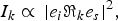
The intensity of a Raman peak of k symmetry is described by the following equation:
76
 is the Raman tensor of the mode k, which is defined according to the symmetry of both the crystal and the mode under consideration.
76
These tensors describe the directionality of the mode with respect to the principal axes of the crystal, thus if a crystal is arbitrarily oriented with respect to the incident/scattered light polarisation vector, the
is the Raman tensor of the mode k, which is defined according to the symmetry of both the crystal and the mode under consideration.
76
These tensors describe the directionality of the mode with respect to the principal axes of the crystal, thus if a crystal is arbitrarily oriented with respect to the incident/scattered light polarisation vector, the
 matrix has to be transformed as
 , where T and T−1 are the transformation matrix of the Euler angles (ϕ, θ, ψ) and its inverse, respectively. The consequence of equation (4) is that, regardless of the relative orientation of the crystal main axis with respect to incident/scattered light polarisation, the crystal will always contribute to the signal intensity up to a certain extent. This is the main difference between Raman and diffraction-based methods, whereby contribution to the measured signal is obtained only when the crystal is aligned with the beam. Consequently, the interpretation of Raman results is less straightforward.
In the past, polarised Raman spectroscopy has been mainly used to determine crystal orientation in semiconductor and insulator single crystals by applying equation (4) without further developments. This has been important to determine the main axes of anisotropy in silicon, 79 diamond,80,81 and to enable Raman mode assignment in materials using several polarisation settings.82-84
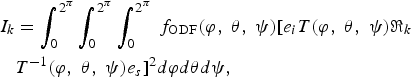
If the material is polycrystalline and the degree of texture varies on the mesoscopic scale (i.e., the case of a piezoceramic), equation (4) has to be modified to take into account the crystalline orientation distribution using a texture model. The Raman signal, in fact, originates from a scattering volume of several µm3, which may comprise not only numerous domains with different orientations, but even grains.85,86 equation (4) can be written as
 are available.88,90,
91
are available.88,90,
91
The fODF can be represented either with analytical functions or with a discrete model. A common analytical approach is using spherical harmonics.
92
Given the assumption of uniaxial symmetry (valid in poled ferroelectrics), few terms are sufficient to represent the ODF:


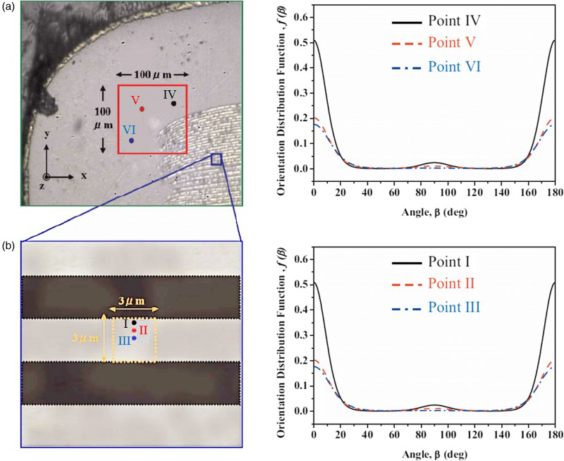
They used this equation to investigate the domain texture in several areas of a barium titanate-based multilayer ceramic capacitor (MLCC) (cf. Fig. 3). They demonstrated that areas within the layered structure have different orientation than in corner areas, and also within each area they showed differences that were ascribed to local residual stresses.
Domain orientation distribution detected by Raman spectroscopy in several areas of a barium titanate-based MLCC. The investigated areas are indicated on the left. The domains display higher degree of orientation in the vicinity of the electrodes. Reprinted with permission from Ref.
93
Although certainly equation (7) can be used for qualitative comparisons between different samples, its application to quantitative analyses is limited. In fact, it was demonstrated
37
that also this approach leads to unphysical results by achieving in some cases greater polarisation texture than theoretically possible in piezoceramics. Röhrig et al. used a discretised approach, in which an ensemble of n domains was assumed as initially isotropic, and the Raman intensity of the whole ensemble was calculated using the following equation:
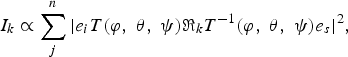
The results of the RMC model were compared with the analytical approach of equation (7) (cf. Fig. 4) on both unpoled and poled piezoceramic polycrystals: The RMC fitting yields nearly the same results as the analytical approach from Okai et al.,
93
with one notable exception: In the poled sample close to the poling axis, the analytically fitted ODF yields higher values at low angles than the RMC fit. This causes an overestimation of the domain distribution at angles close to the poling direction, which could be corrected only by increasing the number of terms in equation (7). Hence, the RMC model seems being more advantageous, since it can reproduce artefact-free ODFs from Raman data.
ODFs calculated by the RMC model of Röhrig et al.
37
(solid black line) and equation (7)
93
(dashed black line) using polarised Raman spectroscopy data measured on both unpoled and poled PZT polycrystalline samples. The theoretical ODF is represented as a thin grey line in both cases. In the poled ceramic, the measured ODF is consistently lower than the saturation value, since the measurements were performed in a remanent state
37
If the material possesses a certain degree of texture that does not vary on the mesoscopic scale, it is possible to use Raman spectroscopy also to measure local domain orientation in spatially resolved fashion. This can be performed with the following procedure: (i) The values of the Raman tensor parameters of equation (4) have to be determined according to a definite texture state.
78
This can be a single-crystalline state but also a textured polycrystalline state, provided that it matches the degree of texture of the material to be investigated. (ii) A spatially resolved analysis (i.e., a linescan or a map) is performed on the surface of the material of interest. (iii) In each investigated point the domain preferential orientation is calculated using equation (4) – where
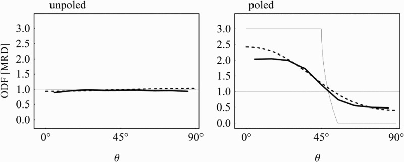
Domain maps by polarised Raman spectroscopy in both a unpoled and b poled PZT polycrystals in the neighbourhood of Vickers indentations showing the domain orientation relative to poling direction and polarisation direction of the laser (collinear with poling direction). In the poled material, domain switching was detected only in proximity of the crack parallel to poling. In the non-poled sample approximately the same amount of domain switching was obtained on both cracks. Reprinted from Ref.47 with permission from Elsevier has to be transformed according to the Euler's angles – and the parameters retrieved in part (i) of the procedure. If the variation of domain orientation is expected to occur only on one angle, it is sufficient to apply equation (4) only to one Raman mode.
47
If all three orientations of the domain vector have to be obtained, a system of equations constructed by applying equation (4) to three distinct Raman modes, or the use of different polarisation configurations, is necessary.
93
Figure 5a and 5b reports Raman maps of in-plane domain orientation obtained in the neighbourhood of the Vickers indentations shown in Fig. 1b and 1c, which were placed on unpoled and poled PZT bulks, respectively. The colour code for the orientation of domains is also indicated. The original orientation, before placing the Vickers indents, was 45° in the case of the unpoled sample and 0° in the poled one. As can clearly be seen, in the poled material the area around the crack parallel to poling underwent domain switching to a much higher extent with respect to the unpoled material or the perpendicular crack, where little or no domain switching occurred. In the unpoled material, domain switching occurred on both cracks up to the same extent. This is very well in accord with the evaluations of CGR reported in chapter 2, thus confirming the role of ferroelastic anisotropy in the toughening of PZT.
47
has to be transformed according to the Euler's angles – and the parameters retrieved in part (i) of the procedure. If the variation of domain orientation is expected to occur only on one angle, it is sufficient to apply equation (4) only to one Raman mode.
47
If all three orientations of the domain vector have to be obtained, a system of equations constructed by applying equation (4) to three distinct Raman modes, or the use of different polarisation configurations, is necessary.
93
Figure 5a and 5b reports Raman maps of in-plane domain orientation obtained in the neighbourhood of the Vickers indentations shown in Fig. 1b and 1c, which were placed on unpoled and poled PZT bulks, respectively. The colour code for the orientation of domains is also indicated. The original orientation, before placing the Vickers indents, was 45° in the case of the unpoled sample and 0° in the poled one. As can clearly be seen, in the poled material the area around the crack parallel to poling underwent domain switching to a much higher extent with respect to the unpoled material or the perpendicular crack, where little or no domain switching occurred. In the unpoled material, domain switching occurred on both cracks up to the same extent. This is very well in accord with the evaluations of CGR reported in chapter 2, thus confirming the role of ferroelastic anisotropy in the toughening of PZT.
47
Discussion
Since modern devices based on ferroelectric ceramics are generally built as composite structures with thin ceramic layers and metal electrodes, the length scale of piezoelectric activity by DW motion is a dominant factor that influences the device's properties. Consequently, the investigation of ferroelectric domain texture across several length scales is mandatory. The techniques we explained in this review can be chosen according to the spatial or volumetric dimensions of the region that has to be analysed.
Macroscopic methods such as indentations are only surface-sensitive, however, the dimensions of the indenter can be varied, and several areas on the surface of piezoelectric devices can be investigated (i.e., the texture difference between active and passive zones in multilayer piezoelectric actuators 96 ). There are several reports on the use of nanoindentation to influence/analyse the domain structure in piezoceramics.97,98
Diffraction-based methods can be chosen depending on the length scale of the area of interest: Laboratory XRD is surface-sensitive and has a spatial resolution of tens of µm; synchrotron XRD averages over the whole thickness of the material, but the location of the beam can be controlled on the µm to sub-µm scale.99,100 Neutron diffraction presents similar capabilities to synchrotron XRD, however the investigation of sub-µm features is at present challenging. 101 EBSD, being it also a surface-sensitive method (up to a maximum penetration of 5 µm 101 ), can be a powerful alternative to laboratory XRD with the capability of producing spatially resolved orientation maps. However, it has the drawback of requiring cumbersome sample preparation.
Raman spectroscopy may overcome the limitations of diffraction techniques. In fact, it is non-destructive, requires little sample preparation, and can detect differences in texture with µm-scale spatial resolution. This method is surface-sensitive, however the depth of penetration can be finely adjusted in semi-transparent materials by using defocussing techniques and a confocal probe. 102 The main problem with Raman is the interpretation of measured data, since a suitable texture-based model for the fitting of the collected spectral intensity is necessary. All in all, the combination of EBSD, laboratory XRD and Raman spectroscopy can be very powerful to analyse scale-dependent texture in piezoceramics, since these methods obtain information on comparable depth but with different spatial resolution.
Lastly, it is worth mentioning PFM. This method is very popular for the determination of the orientation angles of ferroelectric domains on the nanoscale in all three spatial dimensions.103-106 PFM has been also used to study the switching behaviour of DWs in several ferroelectric and multiferroic compositions.104,106 This method, however, has not yet been established to allow reliable determination of a domain ODF. 107 For this reason, PFM has not been reviewed here; the reader is referred to the excellent reviews by S. V. Kalinin et al. 103 ,108
Summary
In this work, several analytical methods to study the microscopic orientation distribution of ferroelectric domains have been reviewed, with a focus on diffraction-based methods and Raman spectroscopy. All methods are distinguished by different capabilities in terms of spatial resolution, penetration depth and requirements for sample preparation. The theoretical background of the methods and the procedure for texture analyses have been detailed, giving also several examples of application. For the study of texture on different length scales, the use of a combination of the presented techniques is the most plausible scenario.
Footnotes
Acknowledgements
The work was supported by the Federal Ministry for Transport, Innovation and Technology (bmvit) and Austrian Science Fund (FWF): TRP 302-N20. Prof. Jacob L. Jones (North Carolina State University) and Dr. Sören Röhrig (Materials Center Leoben) are gratefully acknowledged for fruitful discussions and critical reading of the manuscript.