
Abstract
Selective electron beam melting (SEBM) belongs to the additive manufacturing technologies which are believed to revolutionise future industrial production. Starting from computer-aided designed data, components are built layer by layer within a powder bed by selectively melting the powder with a high power electron beam. In contrast to selective laser melting (SLM), which can be used for metals, polymers and ceramics, the application field of the electron beam is restricted to metallic components since electric conductivity is required. On the other hand, the electron beam works under vacuum conditions, can be moved at extremely high velocities and a high beam power is available. These features make SEBM especially interesting for the processing of high-performance alloys. The present review describes SEBM with special focus on the relationship between process characteristics, material consolidation and the resulting materials and component properties.
Introduction
During the last years, digital manufacturing of metallic components directly from electronic data based on layer-by-layer fabrication has developed from rapid prototyping to additive manufacturing (AM). 1–3 In contrast to conventional fabrication technologies, AM offers much more design freedom. For the first time, the design of the components is no longer strongly restricted by the production method, i.e. individual parts with a high complexity, e.g. cellular structures, complex internal structure or cooling channels, can be realised without taking into account specific design rules. In addition, computer-aided designed (CAD) parts can be subjected to topological optimisation routines 4 and be realised without additional cost. This offers many advantages: complex geometry, weight reduction, short lead time, integration of functions, etc.
Essential for the now starting success of powder bed-based AM of metallic components are the attainable material properties, which were at the beginning poor due to a high level of residual porosity. Nowadays, a variety of metallic alloys and high-performance materials can be successfully processed. The achievable material properties are comparable to those reached in conventional processes such as casting or forming. In addition, there is a high potential of the process-inherent rapid and directed solidification which leads to very fine microstructures and epitaxial growth. Just now, one starts to realise that this opens new possibilities to design components where the local materials properties are adapted to the local requirements. In addition, the high cooling rates open new possibilities in alloy design.
Selective electron beam melting (SEBM) is a powder bed-based AM technology. It was commercialised in 1997 by Arcam AB Corporation in Sweden. At the moment, Arcam is the only company selling SEBM machines. Besides Arcam, there is research activity on self-built SEBM machines, which have up to now not reached the performance of the Arcam machines. 5–8
SEBM belongs to the group of AM technologies that result in fully dense metallic parts. 9,10 It resembles the more common selective laser melting (SLM) process where a laser beam instead of an electron beam is used as heat source. Both are powder bed based layer-by-layer techniques where a powder layer is applied on a building area and selectively molten by a moving heat source. Nevertheless, in detail SEBM and SLM show strong differences resulting from the different nature of the energy that is carried by electrons and photons, respectively. Using electrons as an energy source offers specific advantages and disadvantages. An electron beam can be focused and moved inertia-free by electromagnetic lenses. Thus, the electron beam reaches velocities of up to 105 m/s within the building area, i.e. the beam is able to jump nearly instantaneously from point to point. Hence, with an electron beam innovative heating and melting strategies can be realised. On the other hand, vacuum conditions are necessary and there is a danger of electrostatic charge of the powder, eventually leading to process instabilities. In addition, SEBM is restricted to conductive materials, i.e. metals and alloys.
The aim of this paper is to review the current state-of-the-art of SEBM as used to fabricate metallic components from metals and alloys. The similarities and differences to SLM are discussed. Special emphasis is on the specific properties and possibilities of SEBM. The first part of the paper describes main characteristics of the SEBM process and their implication on the microstructure and materials properties. Based on this, the second part gives an overview of materials that have been investigated by SEBM. In the summary, the application fields where SEBM seems to be inferior to SLM are identified.
Selective electron beam melting
In the following, SEBM is described in detail in order to elucidate the correlation between the SEBM process and the resulting material properties.
Process cycle
Figure 1 shows the building chamber of a SEBM machine and a schematic of the entire process, which is based on CAD data sliced into layers of constant thickness to generate layer information. The process operates under vacuum (10−4–10−5 mbar) which is of particular importance for metals and alloys with a high affinity to gases like oxygen and nitrogen. A small helium pressure (‘controlled vacuum’) of 10−3 mbar is applied to prevent electrostatic charging and so-called smoke events,
5,6
which lead to powder spreading and eventually to process termination. Electrons which are emitted by a hot tungsten filament (Arcam S12, A2, A2x) or a lanthanium hexaboride LaB6 (Arcam Q10, Q20) cathode, are accelerated to 60 keV and focused and deflected with the help of electromagnetic lenses. The beam current is between 1 and 50 mA resulting in a maximum beam power of about 3 kW. In contrast to the tungsten filament, where the beam diameter (ca. 350 µm) strongly increases when the beam power exceeds 1 kW, the beam produced with a LaB6 cathode is much more stable. The width of the beam is nearly constant up to powers of 3 kW. Nevertheless, the LaB6 cathode is very sensitive to smoke events and is actually only applied for processing of titanium. SEBM process. Left: Process chamber. Right: 4-step process for building one layer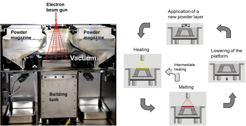
The component is built layer-by-layer. Each layer is generated in four steps, see Fig. 1, right. After completing the last layer, the component cools down within the machine. Cooling is normally accelerated by flooding the process chamber with helium.
Application of the powder
In the first process step, a thin powder layer is applied with a stainless steel rake on the building area (maximum size depends on the machine, ∼ 250 mm × 250 mm). The powder is supplied by two powder magazines which are located above the building plane. The thickness of the powder layer is chosen based on the aimed layer thickness (between 50 and 150 µm). The very first layer is applied on a preheated start plate, typically stainless steel. The preheating temperature is slightly above the building temperature. In order to prevent contamination, especially when processing high-performance materials, the plate material and the building material should be the same or similar.
Generally, the powder properties are essential for process stability and determine resulting materials properties. The flowability of the powder, characterised by the apparent density and the tap density, should be as high as possible. Normally, spherical gas atomised powders are used, see Fig. 2. The recommended powder size is between 40 and 105 µm. Powders with a much smaller mean diameter lead to process instabilities whereas larger ones can be used. The fraction of smaller particles and especially of small satellites should be as small as possible due to a strong reduction of flowability, density and electric conductivity. This is the reason why powders produced by PREP (plasma rotation electrode)
7
are used since their flowability is higher due to a perfect round shape without satellites.
a Typical particle size distribution of a gas atomised powder (here: CMSX-4), b Ti–6Al–V4: SEM of the powder particles. Non-spherical particles, particle agglomerates and satellites are visible. c Sintered powder block (Ti–6Al–4V), d c after removing the powder by sand blasting with the same powder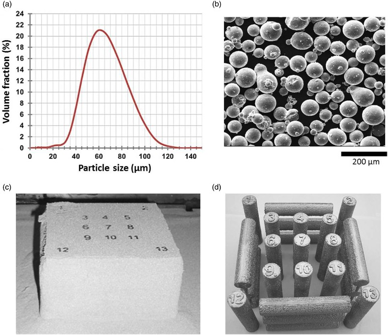
Heating
During the heating step, the applied powder is heated by scanning the electron beam several times across the layer. This step is crucial and has two aims, to deliver energy to maintain the temperature within the building volume, TB, and to sinter the powder particles slightly. The latter is essential to increase electric conductivity of the powder to prevent process instabilities like ‘smoke’ where the powder gets distributed within the machine due to repulsion of the charged powder particles.
11
Normally, a smoke event leads to the termination of the process. During heating, the defocused electron beam scans the building area several times with velocities of about 10 m/s while the beam power P is successively increased to about 3 kW, see Fig. 3
a. Preheating temperatures and strategies not only depend on the metal or alloy but also on the powder properties. Generally, TB (measured with a thermocouple at the starting plate) varies between 300 °C for pure copper
12
and up to 1100 °C for intermetallic phases
13
or some nickel-base alloys. If the fraction of fine particles in the powder is high, preheating has to be performed very carefully in order to prevent smoke. Heating and melting during SEBM. At the top: photograph during the process. At the bottom: schematic of the beam movement. a Heating by quasi-multi-beam scanning of the total building area with a defocused beam, b Melting by hatching, c Quasi-multi-beam contour melting by jumping from point to point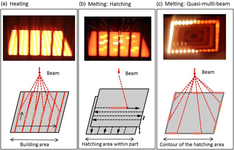
The building temperature and preheating strategy cannot be directly derived from the melting temperature of the alloy. On the one hand, elevated temperature stabilises the powder bed because this provokes sintering. The velocity of the sinter process is governed by the exact alloy composition, since this determines the constitution of the surface oxide layer of the powder particles. On the other hand, heating to high temperatures is also necessary if the alloy is prone to crack formation which depends on the mechanical properties of the alloy and the kinetics of precipitate formation.
The high building temperatures have a high impact on the residual microstructure and stresses. Compared to the laser-based AM processes, 14 which are usually performed at much lower temperatures, the level of residual stresses is lower 15 and the SEBM microstructure is coarser due to the reduced cooling velocities and temperature gradients. 16
As a result of this heating step, the samples are embedded within a slightly sintered powder bed after the build has been finished (see Fig. 2 c). The powder can be removed and separated by sand blasting using the same powder particles as blasting abrasive since the level of sintering is still very low: pronounced sintering necks are not yet present (Fig. 2 d). Generally, the powder can be nearly completely recycled and reused 17 if appropriate processing conditions are applied. Powder loss is very low and mainly the result of partially molten powder particles sticking together. These agglomerates have to be removed by sieving before the powder can be used again. The powder properties change a little bit in each process cycle since the small satellites are more and more removed. This improves flowability and process stability.
Melting
After preheating, the electron beam scans the powder layer with lower velocity (typically 4 m/s) and melts the powder particles where solid material is to form, see Fig. 3 b. Melting of areas and contours is distinguished. There are a plenty of process parameters which have to be defined: beam power P, beam velocity v, distance between lines d, focus offset of the beam, number of contours, etc. Melting of areas is generally by hatching where the direction of the beam changes in each line and also in each layer by 90°. In addition, SEBM allows contours to melt in the so-called quasi-multi-beam mode where the contour is molten quasi simultaneously at up to 100 points by point to point jumping of the beam, see Fig. 3 c. This strategy is applied in order to increase the surface quality, i.e. to reduce roughness.
Material consolidation
SEBM is a deposition welding process with about 102–103 m weld seam per cm3. Thus, SEBM shows phenomena usually observed for welding processes. 18 Generally, the process parameters typically used during SEBM lead to a heat conduction driven welding process with only a small tendency to deep welding. 19
One important difference between SEBM and SLM results from the absorption of the beam. The way how energy is absorbed is essential since it not only determines the amount of energy deposited but also whether superheating and evaporation takes place. The latter determines the welding mode, namely heat conduction welding or keyhole welding, and the resultant composition of the alloy due to selective evaporation. Photons are absorbed or reflected within some nanometers at the surface of the material whereas electrons deposit their kinetic energy within a depth of some micrometers 20 which is about three orders of magnitude larger. Therefore, for SLM strong evaporation and reflection of laser radiation is always an issue, especially for some highly reflective materials such as pure copper and copper alloys.
Energy dissipation of the incident electrons in matter is a function of their energy (the acceleration voltage), the atomic number of the material (the penetration depth decreases with increasing atomic number) and the angle of incidence. 20 A phenomenological model to describe the absorption of an electron beam within a powder bed is described in Klassen et al. 21 The energy is converted into heat and eventually the powder particles melt, coalesce and form an agitated melt pool for some milliseconds. 6,22 Fluid dynamics is mainly driven by capillary forces and back pressure due to evaporation.
In order to obtain completely dense materials, the melt pool must reach a critical depth which is much higher than the layer thickness. In experiments, about 3–4 times the layer thickness has to be molten in order to prevent the formation of faults, i.e. non-molten powder or non-connected layers. 19 Numerical simulation shows that this is related to the surface roughness leading to strong local variations of the thickness of the new powder layer. 23 Nevertheless, applying appropriate process parameters, the density is higher than 99.5 %. Very often, some round pores resulting from enclosed gas bubbles within the powder particles are observed. 9,24 The microstructure and the mechanical properties of the consolidated materials depend strongly on the processing parameters (T0, P, v, scan length, etc.). The same material processed with different parameter sets and scanning strategies may either be isotropic or show a high texture, 25 fine or coarse grained 26–28 and a homogenous or inhomogeneous chemical composition. 7,29,30
Composition inhomogeneities result from selective evaporation of elements with a low vapour pressure. Since heating is up to very high temperatures and the process works under vacuum conditions, evaporation has to be taken into consideration. There are two evaporation effects, which have impact on the material and component quality. On the one hand, the vapour back pressure in combination with the surface tension may relocate material.
30,31
As a consequence, the resulting melt surface is not flat but shows varying depths. This effect is already visible in a single weld seem. Material accumulates at the beginning and is thus missing at the end. The same effect is present during SEBM. It depends on the melting strategy whether pronounced material accumulations develop. If the material displacement is larger than the layer thickness, the new applied powder layer will not cover the bulges. During melting of the following layer, material is displaced again in the same pattern if the melting strategy is not altered. Consequently, the bulges grow with each layer which eventually leads to the termination of the process. Figure 4
a shows a good melt surface compared to one where a characteristic pattern emerges as a function of the processing parameters. This effect is well known and also commercially used under the trade name Surfi-Sculpt® (by TWI) to pattern surfaces by multiple melting. Evaporation effects: a Exemplary melt surfaces of 15 × 15 × 10 mm3 cubic samples. Left: good surface, right: poor surface with a characteristic pattern induced by material displacement, bottom: Simulation to illustrate the mechanism of melt displacement. The beam moves from left to right up to 16 times leaving behind a built-up area and a deep hole. b Element mapping showing the Al distribution in Ti–48Al–2Cr–2Nb, c Layered microstructure as built in Ti–48Al–2Cr–2Nb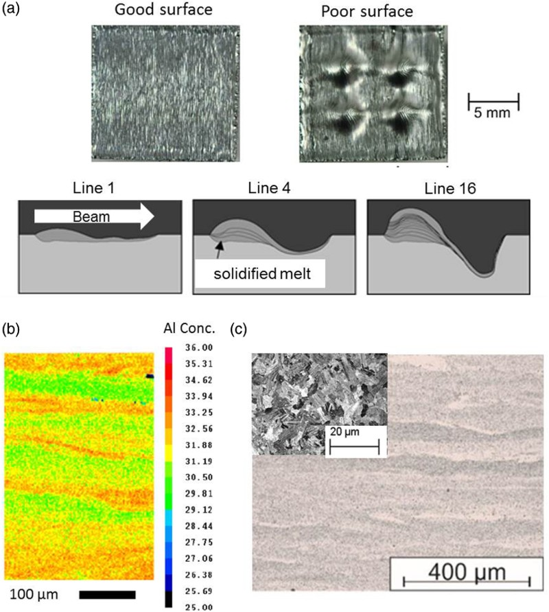
Some elements including aluminium and zinc show a very high vapour pressure. As a result, these elements may strongly deplete at the melt pool surface if the maximum temperature is high (the latter condition is normally fulfilled for standard processing parameters as recommended by Arcam). The resulting composition inhomogeneities 30 are partially compensated by melt convection but lead to element distributions as shown in Fig. 4 b. The total aluminium content is strongly reduced and the aluminium distribution, i.e. the alloy composition, varies in layers. For sensitive materials, e.g. titanium aluminides, this local change of the composition has a strong impact on the as-built microstructure (Biamino S. K., 2014), see Fig. 4 c. The local variation of the aluminium content leads in particular to a variation of the phase transition temperatures and the phase composition.
The successive building process in thin layers by local heat input leads to characteristic microstructures due to rapid and directional solidification. Solidification is mainly directed in building direction and predominantly epitaxial, see Fig. 5.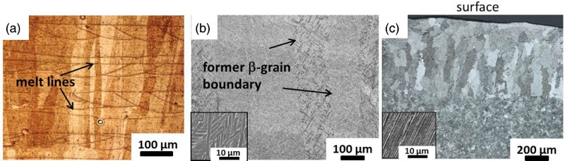
As-built SEBM components reflect their production history. In Fig. 5 a even the melting strategy, i.e. the hatching procedure, is visible. The grains are observed to grow across hundreds of layers, Fig. 5 a and b. As a result, SEBM samples very often show a strong texture combined with anisotropic properties. 25,32,33 Grains with favourable orientation overgrow unfavourable oriented ones. Typically, the grains are oriented in the <001> direction for alloys which solidify starting with a face centred cubic (fcc) or bcc phase. The width of the columnar grains depends on the processing conditions and increases with increasing melt pool size. 34
There are different mechanisms provoking the formation of new grains. New grain formation typically starts at the boundary of the component where partially molten powder particles act as new nuclei. Also specific melting strategies may cause new grain formation. 25 A classical CET (columnar-equiaxed-transition) with the appearance of new grains may be artificially induced by very high energy input but this is generally not observed when using standard building parameters.
Microstructure and in-situ heat treatment
In addition to solidification and cooling, in-situ heat treatment, which is characteristic for SEBM, exerts a strong influence on the resulting microstructure. Generally, SEBM operates at high building temperatures, namely around 300°C (pure Cu), 600°C (Ti) or 1100°C (TiAl). These high temperatures have a high impact on the microstructure and the residual material properties. In addition, the as-built properties are position-dependent due to the different heat treatment conditions within the building chamber. Figure 6 shows a schematic of the temperature-time history at a fixed point of the component. In-situ heat treatment during SEBM: Schematic of the temperature evolution at a fixed point of the component where the beam passes several times in each layer. A simulated temperature evolution at different depths (in steps of 100 µm) for Ti–6Al–4V is shown to visualise the time scale of temperature variation near the surface during and after melting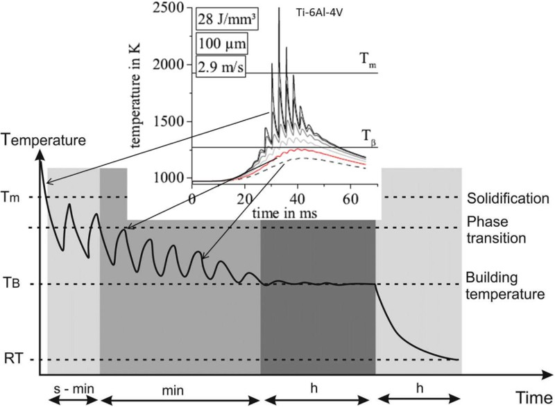
After final solidification (during SEBM, the material is molten several times), the temperature still strongly oscillates due to the melting of neighbouring lines and subsequent layers. A more or less constant building temperature is not reached until 10–20 layers are built upon the observation point. This oscillating temperature period takes about 10–20 minutes. Near the building plane, the temperature approaches several times the solidification temperature and may pass through a number of phase transitions, see simulated temperature evolution in Fig. 6. In addition, homogenisation of the microstructure and aging may take place. The particular processes, e.g. solid state phase transformations, homogenisation, etc., depend on the underlying alloy and the processing parameters.
SEBM of materials with phase transformations in the solid phase provides a means to break up the textured columnar, as-deposited structure. 33,35 During cooling to building temperature, one or more phase transformations may be passed through due to the inherent in-situ heat treatment, see Fig. 6. These phase transitions can destroy or reduce the texture, see Fig. 5 b and c. Since solidification of the titanium alloy Ti–6Al–4V (Fig. 5 b) is via the β phase, the initial columnar β grain structure is still visible although the β phase transforms into a α−β microstructure when the temperature falls below the β transition temperature. 35 This effect is even more pronounced for the titanium aluminide alloy, Fig. 5 c. After the initial epitaxial solidification from the melt (creating columnar grains at the surface), the sample is exposed to successive heat treatments by the deposition of the neighbouring lines and next layers. In this heat-affected zone the material temperature may exceed once or several times the α transition temperature from which it is cooled down into the two phase α−γ region leading to a refining of the microstructure. 13
Generally, the resulting microstructures are very fine and far from equilibrium since SEBM solidification rates and temperature gradients are very high (108–109 K/m, 104–105 m/s from numerical simulation). The solidification rates and the resulting microstructures depend on the amount of energy which is deposited and on the scanning strategy. The dendritic arm spacing is typically a few microns, see Fig. 7
a. These values are somewhat higher than for SLM microstructures where the cooling rates are even higher due to thinner layer thicknesses and smaller laser spot diameters.
2
Nevertheless, SEBM segregations are on such a small length scale that some homogenisation can already take place during the building process due to in-situ heat treatment. Figure 7 displays this effect using the example of the superalloy CMSX-4. The sample depicted in the middle shows the typical columnar grain growth across hundreds of layers. At the top of the sample, i.e. within the last layers which were built, the sample appears opaque due to the presence of strong segregations. Depending on the processing conditions (e.g. building temperature or the beam energy), these segregations become blurred with increasing depth (left bottom).
16
In-situ heat treatment during SEBM: a Nickel-base alloy CMSX-4 (schematic). Middle: Micrograph of the sample with elongated grains. Left: Homogenisation (LOM), Right: Aging of the γ’-particles (SEM) (see also Ref. 16), b Nickel-base alloy IN718: the niobium-rich δ-phase is precipitated in the interdendritic areas with columnar architecture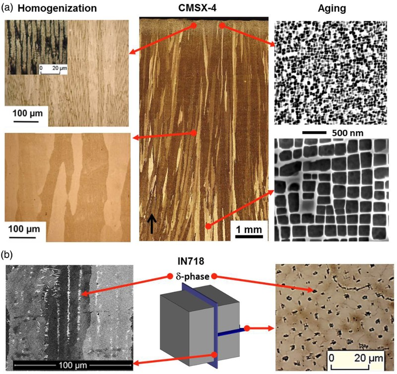
In-situ heat treatment during SEBM can also lead to the nucleation and growth of precipitates. 16,36,37 Figure 7 (right) shows the γ/γ′ microstructure with the typical cuboid-shaped γ′-precipitates in CMSX-4. The growth of the γ′-precipitates with increasing build time, i.e. with increasing distance from the surface, is clearly visible. Due to the long processing times and high temperatures, aging is an issue and has to be taken into account. A further example is the growth of the niobium-rich δ-phase in IN718 (Fig. 7 b) which is even pronounced if cooling from the building temperature to room temperature is artificially slowed down. 36,37 Generally, these phases are distributed not homogenously but form columnar precipitate architectures due to self-organisation phenomena during solidification. 18 Given the high solidification rates, solidification is cellular or only slightly dendritic. Since niobium is segregated during solidification within the interdendritic areas, nucleation of the δ-phase occurs preferably there. As a result, the distribution of the δ-phase reflects the directional columnar solidification structure.
Distortion, residual stresses and surface roughness
Component precision is one of the challenging topics for AM. There are different factors influencing precision: mean powder diameter, beam diameter, shrinking and distortion due to thermal shrinkage and residual stresses. Figure 8 shows a Ti–6Al–4V T-beam with supports where the geometric deviations due to shrinking are clearly demonstrated. The increasing bending of the originally perpendicular supports indicates thermal shrinkage which influences the definition of the edges. The deviation Δx increases linearly with the length l and eventually vanishes with increasing height of the metal beam. Distortion and surface roughness of a T-beam made of Ti–6Al–4V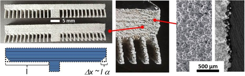
The distortion of the metal beam after it is removed from the start plate is virtually zero or very small since the long building times at high temperature lead to stress-relief annealing and low levels of residual stresses. This is an essential difference to SLM samples which are generally built at much lower temperatures. 15 As a result, there is a high level of residual stresses in SLM materials. In addition, due to this lower stress level induced by SEBM, the number and density of support structures is usually lower compared to SLM.
The process parameter settings and sample thickness have a strong effect on the surface roughness of the produced parts. 38 The effect of the process parameters settings on surface roughness of Ti–6Al–4V is investigated in Syam et al. and Jamshidinia and Kovacevic. 39,40 Generally, the roughness values Ra and Rq vary for the samples of different thickness and for samples built with different parameters. This is why the values given in the literature for Ra and Rq are not coherent. Compared to SLM parts, the SEBM roughness values are much larger. Typical values are Ra = 11 µm and Ra = 25–35 µm for SLM and SEBM, respectively. 1 The higher roughness for SEBM compared to SLM results from larger powder particles, a larger layer thickness and a larger beam diameter.
Materials
SEBM materials
Generally, nearly 100 % density can be reached for metals and alloys if appropriate process parameters are used. Regarding the materials properties, it is essential to differentiate between as-built, heat treated and hot isostatic pressed (HIP) (+ heat treated) materials. In addition, texture may lead to direction-dependent properties. Since the surface roughness is high, there is a strong difference between non-machined and machined samples. Especially for the as-built material, the position within the build chamber has a strong influence on the resulting properties. Nevertheless, during the last decade it has been demonstrated that SEBM materials can reach properties similar or superior to wrought materials due to the rapid cooling conditions leading to a fine microstructure.
Pure iron and steel
From a historical viewpoint, the processing of large and voluminous steel parts was the initial motivation to use an electron beam as energy source. Thus, at the beginning of commercialisation, Arcam’s advertising strategy was based on the high power of the electron beam able to consolidate a large volume of steel per hour. Using SEBM for production of tool steel, injection mould inserts were considered as a promising field of application. Nevertheless, the focus completely changed during the last decade and Arcam’s focus is now on titanium and titanium alloys; steel is now hardly a topic.
Altogether, the literature on SEBM of iron and steel is rather scarce. The microstructure and properties of pure iron processed by SEBM are described by Murr et al. 48 In an initial study Cormier et al. 52 presented a microstructural analysis of H13 tool steel produced via SEBM. The parts exhibited full interlayer bonding with virtually no porosity. Due to the high cooling rates, the as-built material was martensite with a hardness of 48–50 HRC. In Refs. 50 and 51 an Arcam SEBM H13 insert with complex cooling geometries is compared against traditionally cooled inserts. The improved cooling rates shown by SEBM inserts over conventionally cooled core inserts offer improvements with respect to the productivity and dimensional accuracy.
The formability of 316L stainless steel by SEBM was first investigated by Qi et al. 49 Gas atomised powder with particle sizes of 70–100 and 40–63 µm and water atomised powder with particle sizes of 10–40 and 40–63 µm were investigated. Generally, the water atomised powder shows a stronger tendency to balling than gas atomised powder. The microstructure is found to be fine and compact with metallurgical bonding between layers. The latest publication from the same group 14 addresses the influence of the scanning strategy on densification and the surface roughness. Uniform microstructures with densities of about 99.96 % can be reached. Mechanical properties are not reported.
Titanium base alloys
Most of the SEBM research activity is on titanium and its alloys, especially Ti–6Al–4V. The vacuum conditions of SEBM result in a nearly perfect protection against contamination with gases, particularly oxygen. The measured oxygen content within SEBM Ti–6Al–4V fulfils the standard (ASTM F 1108) for Ti–6Al–4V castings. Also multiple use of the powder has been investigated. 17
In SEBM titanium parts, the primary β-grains are still visible although the texture is nearly completely destroyed by the α−β phase transition, see Fig. 5
b. The microstructure is dominantly α/β. The primary β phase firstly transforms into α′-martensite and then decomposes into α/β in continued deposition since α′-martensite is only found within a small thickness near the top.
31
This is different for SLM, where α′-martensite is present all-over the as-built samples due to the higher cooling rates and the lack of in-situ heat treatment.
2
The grain structure and texture in Ti–6Al–4V is comprehensively discussed by Al-Bermani
35
and Antonysamy
33
who reconstructed the primary β-phase from α-phase EBSD data. The far weaker α-texture in the final product arises from the phase transformation during cooling giving a near random distribution of α−lamella across the 12 variants possible from the Burgers relationship. The thickness of the α−lamella is determined by the energy input, the building temperature and the resulting cooling conditions. With increasing energy input or building temperature, the α−lamella thickness increases while the yield stress decreases,
28,31,35,55,79
see Fig. 9. Influence of the building parameters on the microstructure and properties of Ti–6Al–4V. Top: Microstructure for different beam velocities and total energy input per volume. Bottom, left: Thickness of the α–lamella as a function of the volume energy. Bottom, right: Strength as a function of the α–lamella thickness (adapted from Ref. 28)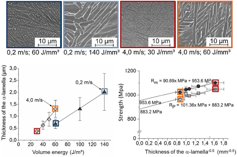
Thus, the mechanical properties vary locally 26 since the local thermal conditions are strongly dependent on the position within the part and the distance from the starting plate. 27,31
Literature data about the mechanical properties of SEBM Ti–6Al–4V show a large spread, 80 especially regarding the elongation to fracture. This is due to the fact that the quality of the tested samples is sometimes insufficient, i.e. there are still binding defects between subsequent layers present. If the process parameters are chosen well, the samples are free of binding defects and SEBM has the ability to produce parts comparable in strength and elongation to the very best titanium wrought products. Elongations achieved by SEBM can be from roughly 23–92 % greater than the average elongation for high-strength Ti–6Al–4V forgings. 27
Fatigue properties determined for as-built specimens (no heat treatment, no surface treatment) show that the rough surface has a strong negative influence on the fatigue resistance. 81 Cracks are initiated from the root of the notch at the grooved surface between the layers, especially if the direction of stress is parallel to the orientation of the electron beam. Therefore, the fatigue properties of as-built samples strongly depend on the direction of load compared to the building direction.
Nickel-base alloys
Currently, nickel-base alloys attract strong attention throughout the AM community. These high-performance alloys are characterised by excellent mechanical properties, a high resistance to creep deformation and corrosion or oxidation. Due to these properties, these alloys are mainly applied in power plants or aero engines. 82
Generally, nickel-base alloys can be roughly divided into weldable and non-weldable alloys. The latter are highly prone to crack formation due to a high amount of the strengthening γ′-phase. Thus, non-weldable alloys are difficult to process by SEBM or SLM, which are basically welding processes. The advantage of SEBM compared to SLM is the possibility to work at very high temperatures (up to 1100°C at the starting plate) by heating the samples with the electron beam from above. In this way, also alloys which are generally considered as non-weldable can be successfully processed by SEBM.
From the group of weldable nickel-base alloys, IN625 and IN718 have been processed by SEBM. IN625 is a commercial columnar-grained, gas turbine alloy characterised by a high strength, excellent workability and excellent corrosion resistance due to its high chromium content. Figure 7 b shows the typical columnar precipitate architecture observed in SEBM processed IN718 (for IN625 see Murr 18 ). Lines of precipitates, parallel to the elongated grains, are present on grain boundaries and within grains. The formation of precipitates is primarily in highly segregated regions resulting from cellular/dendritic solidification where elements like Ti, Nb, Ta and Mo concentrate in the last remaining liquid, triggering the formation of precipitates there. Generally, there is a strong correlation between the orientation of the γ grains and the orientation of precipitates. 18,32 In IN718 or IN625 these precipitates are γ″ Ni3Nb disk platelets coincident with Ni–Cr (fcc) {111} planes, see Fig. 7 b.
Strondl et al. 32 were the first to investigate the microstructure evolution and to perform phase analysis of IN718 produced by SEBM in the as-built state. IN718 consists of a fcc γ-matrix which is strengthened by several phases including carbides and intermetallic compounds (fcc γ′ Ni3(Al, Ti, Nb), ordered tetragonal γ″ Ni3Nb). In addition, topologically close-packed phases such as Laves phases, the orthorhombic δ-phase and the tetragonal σ-phase can develop. The matrix of as-built IN718 consists of columnar γ grains with <001> orientations parallel to the direction of building. A comprehensive discussion of the effect of in-situ heat treatment on microstructural heterogeneity of IN718 is given by Sames et al. 36 The processing window for IN718 and the correlation between different processing parameters within the processing window and the resulting microstructures is described by Helmer et al. 19
The influence of the processing strategy on the grain structure and mechanical properties is investigated by Körner et al.,
25,34
see Fig. 10. Applying specific melting strategies, the grain structure can be either columnar or equiaxed. Thus, switching from an isotropic material to a strongly anisotropic material by changing the processing parameters is possible and can be used for local optimisation of materials properties within components. This opens the future prospect not only to optimise parts with respect to their topology but also with respect to their local materials properties. Influence of different processing strategies on the grain structure of IN718. SEM-micrograph showing a columnar grain structure a and an equiaxed grain structure b in a longitudinal section parallel to the building direction (for details see Ref. 25)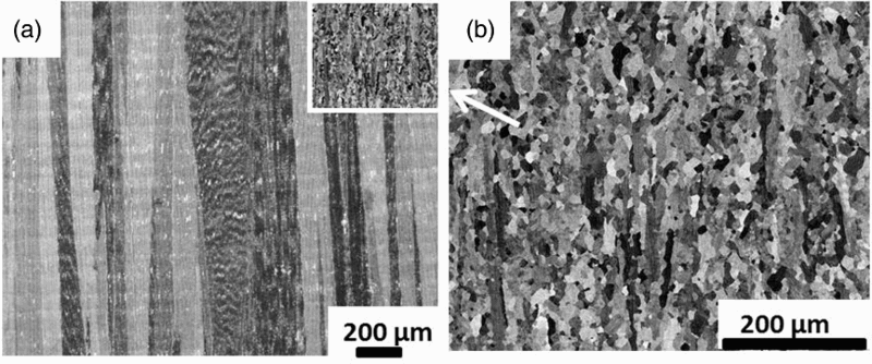
From the group of non-weldable nickel-base alloys, the columnar alloy Rene 142 18,54 and the single crystalline alloy CMSX-4 16 have been investigated. Both alloys show a high volume fraction of γ′ precipitates in the as-build state, see Fig. 7 a. For Rene 142 the γ′ size is reported to be about 275 nm with a volume content of 59 %. 54 The influence of the process-inherent in-situ heat treatment on the size of the γ′ precipitates is not addressed. Solution heat treatment of the single crystalline alloy CMSX-4 produced by SEBM is compared to that of conventional cast CMSX-4 by Ramsperger et al. 16 In SEBM materials, segregations are on the micrometer scale and thus about two orders of magnitude finer than in conventional cast materials. As a result, homogenisation of the material (it is not completely homogenised in the as-built state) can be performed in minutes instead of hours. In principle, SEBM allows the production of components which are essentially free of segregations. The influence of this extreme homogeneity on the mechanical properties is currently under investigation.
Cobalt-base alloys
The first Co-alloy systems, mainly based on Co–Cr–Mo, were developed in the 1930s and are now available under the tradenames Vitallium (60.5 wt.-% Co, 31.5 wt.-% Cr, 6 wt.-% Mo) or Stellite ( Co–Cr–Mo plus W and C). The high amount, about 30 %, of chromium provides these alloys with a high resistance to corrosion and a high hardness. By the addition of carbon, different classes of carbides containing Co, W or Mo in place of Cr are formed, which give these alloys a high strength and further increase in hardness. Typical fields of application are as bearing materials or as high temperature and high wear resistance materials: artificial joints, dental prosthesis, parts of turbo chargers, cutting tools, aerospace fuel nozzles, etc. 82
The traditional way to process Co-base alloys is by casting or forging and subsequent heat treatment in order to adjust the mechanical properties. Although the fabrication of individualised dentures made of cobalt-base alloys by SLM is already performed successfully by several industrial companies (e.g. DeguDent) research activity on this alloy class in the field of SEBM is rather scarce. Fundamental and applied research involving the fabrication of Co–26Cr–6Mo–0.2C components by SEBM is presented in Gaytan et al. 41 and Gaytan et al. 42 The focus of this initial work is on optical microscopy and transmission electron microscopy to investigate the arrangement of carbides and lattice defects. A more comprehensive investigation of Co–Cr–Mo fabricate by SEBM was performed by Sun et al. 43,44
The properties of Co–Cr–Mo alloys are strongly dependent on its microstructure, which is largely determined by the thermal history. At high temperature, the fcc γ-phase is stable whereas the hexagonal ε-phase (hcp) is the stable phase at low temperatures. The temperature-time history is essential for the resulting microstructure since the γ-phase can also be present as a metastable phase at low temperatures. During SEBM, Co–Cr–Mo alloys solidify via the fcc γ-phase which is not or only partially transformed into the stable ε-phase during the building process. The as-built samples show a pronounced texture 43 as a result of epitaxial growth with preferred grain orientation of the γ-phase in <001> direction. The M23C6 precipitates (M = Cr, Mo, Si) are aligned along the build direction with a mutual distance of about a few microns. 41–43 The distribution of the precipitates is the outcome of segregation caused by cellular solidification. The distance between the carbide columns is determined by the solidification conditions, analogous to Fig. 7 b.
After aging at 800°C for 24 h, the γ-phase (fcc) is transformed into the ε-phase (hcp), the grains tend to be equiaxed and the pronounced texture of the as-build sample vanishes. 43 This phase transformation can also occur due to the process-inherent in-situ heat treatment leading to a height-dependent microstructure. 44 Gaytan et al. 41 perform heat treatment according to ASTM F7 CoCr alloy standard consisting of hot isostatic pressing at 1200°C for 4 hours in Ar followed by a quench from a homogenising treatment at 1220°C for 4 hours in Ar at 75°C/min. The resulting microstructure consists of an equiaxed fcc grain structure with the M23C6 precipitates located preferentially at the boundaries of the equiaxed grains and essentially no matrix carbides.
The resulting mechanical properties depend strongly on building and heat treatment conditions. Generally, as-built samples show a strong anisotropy caused by epitaxial solidification leading to a pronounced texture. In addition, the development of precipitates such as carbides is time and temperature dependent. Thus, the properties depend on the z-position (building direction) within the building chamber. The influence of phase composition and grain size inhomogeneity on the creep behaviour of a Co–Cr–Mo alloy is examined in Sun et al. 44 After adequate heat treatment (hot isostatic pressing + homogenisation) Co–Cr–Mo alloys built by SEBM show superior properties compared to wrought or cast alloys. 41
Copper and copper alloys
Copper and its alloys are characterised by a very high electric and thermal conductivity making them ideal candidates for electrical and thermal management systems. These properties combined with the design freedom of AM open new perspectives, especially for complex heat exchanger devices. Generally, AM of copper is challenging due to its high thermal conductivity which leads to a very rapid heat dissipation. In addition, the reflectivity of copper to laser light is very high, which makes SLM of copper difficult 2 and limits the process to copper alloys with a much lower thermal conductivity and lower reflectivity.
In contrast to SLM, SEBM of copper works quite well since the absorption and reflection mechanisms of electrons are different from those of photons. Thus, most of the energy is deposited within the material in SEBM. The energy available is sufficient to consolidate even very pure copper with very high thermal conductivity of 400 W mK−1. In addition, the sintering step, which is obligatory during SEBM, can be extremely short for copper due to its high electric conductivity. Due to the high sintering activity of copper, there is in fact the danger that the powder cannot be removed if preheating is too high or too long. Figure 12 a shows a pure Cu component with a cellular core. Components from Cu are especially interesting for designing effective heat exchangers. Cellular structures from 99.8 % Cu containing Cu2O precipitates and residual oxygen as a consequence of the atomisation production process were investigated by Ramirez et al. 47 In that contribution periodic as well as stochastic open-cell structures are produced and characterised with respect to their stiffness.
Generally, Cu is very sensitive to oxidation and this has to be considered during storage and handling. The effect of a relatively impure (98.5 %) Cu (atomised) precursor powder containing a high concentration of Cu2O was investigated by Ramirez et al. 46 Due to directional solidification during SEBM, precipitation-dislocation architectures are observed. These precipitation-dislocation architectures increase the hardness from a base-plate value of HV 57 to an SEBM product hardness of HV 88.
With increasing oxidation level of the powder, the building temperature (< 400°C for fresh powder 12 ) and preheating time increases and the electric conductivity of the bulk material decreases. Therefore, the quality of the powder is essential. The microstructure of a pure copper sample is depicted in Fig. 5 a. Different layers and individual lines can be distinguished. In addition, epitaxial solidification leads to continuous grain growth across many layers.
Titanium aluminides
γ-TiAl alloys are considered as good candidates for the partial replacement of Ni-base superalloys at temperatures between 600°C and 900°C due to their low density, high specific yield strength, high specific stiffness and good oxidation and creep properties. Classic applications are turbine blades, turbo charger wheels and valves for combustion engines. 83 γ-TiAl-based alloys continue to attract significant attention encouraged by the commercial application of the low pressure turbine blade on the GEnx engine which powers Boeing 787 and 747–8 aircraft. 84
Conventional processing of titanium aluminides is very complicated and represents the main obstacle for a more widespread application of this class of materials. In addition, the properties of γ-TiAl alloys are strongly dependent on their microstructure which can be designed by an appropriate process control and heat treatment. 85 Generally, four different types of microstructures are distinguished: near-gamma, duplex, nearly fully lamellar and fully lamellar.
Also SEBM of titanium aluminides is a challenge since the building temperatures are clearly above 1000°C (∼1100°C). These high temperatures require a sophisticated process strategy and thermal management in order to maintain process stability. Due to the high temperatures, crack formation, observed for SLM,
86
can be completely prevented by SEBM.
7
In a first preliminary paper, Cormier et al.
57
reported the successful fabrication of dense γ-TiAl samples by SEBM using pre-alloyed Ti–47Al–2Cr–2Nb powder. For the processing parameters used by Cormier et al., a significant amount of aluminium (6.1 %) evaporates during densification due to strong local overheating. In the following work of Murr et al.,
58
first results of the microstructure and the hardness of Ti–47Al–2Cr–Nb fabricated by SEBM were presented. The first more systematic approach was made by Biamino et al.
56
for Ti–48Al–2Cr–2Nb. They report that impurity pickup is very low and microporosity can be kept below 2 %. Evaporation leads to aluminium loss of about 1 wt.-% compared to the starting powder. The microstructure is very fine and homogenous due to the high solidification and cooling rates, see Fig. 11. As a result, the materials properties of SEBM γ-TiAl appear very consistent with small scatter. Typical small spherical defect in EBM γ-TiAl specimens a; as-built microstructure after EBM b; microstructure after HIP c; microstructure after thermal treatment d (courtesy of Ref. 56)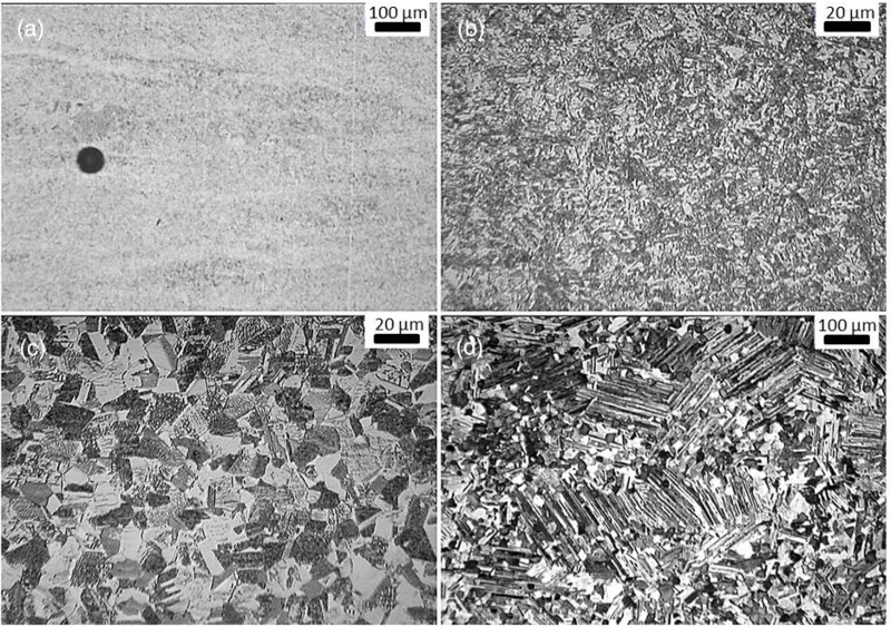
The influence of the processing parameters on the density and as-built microstructure of the samples was first investigated by Schwerdtfeger et al. 13 The line energy necessary to obtain dense samples (porosity < 0.5 %) decreases with increasing beam velocity. The microstructure and the composition of the dense samples are strongly dependent on the total energy input due to the process-inherent heat treatment and maximal temperatures. High line energies lead to a more or less fully lamellar microstructure since the temperature after solidification exceeds the alpha transus temperature. By decreasing the line energy, the lamellar structure disappears gradually. XRD measurements show that the fully lamellar structure present at high line energies transforms to a near-gamma structure with very small grain size at low line energies.
Generally, the as-built samples have to be heat treated to adjust the microstructure and thereby the mechanical properties. A duplex microstructure results from a 2 h heat treatment at 1320°C (below the alpha transus temperature), see Fig. 11 d. If heat treatment is above the alpha transus temperature, a fully lamellar structure develops with a α/γ colony size of several hundred microns.
The major disadvantages of titanium aluminides compared to nickel-based alloys are their poor resistance against fatigue crack growth, their low ductility and low fracture toughness. The investigation of Filippini 87 indicates that γ-TiAl produced by SEBM show a higher fatigue threshold and strength compared to γ-TiAl produce using competing technologies such as casting or powder metallurgy, since typical defects can be avoided. Generally, data now available for SEBM γ-TiAl indicate that it is possible to generate similar or even better mechanical properties by SEBM compared to other fabrication technologies. Nevertheless, the investigations are still at the beginning and more work is needed to generate a comprehensive understanding of the correlation between processing parameters, microstructure and properties for these alloys.
Niobium
Martinez et al. 53 were the first to fabricate niobium SEBM samples. The ability to manufacture Nb components by SEBM may be used for the fabrication of complex superconducting components. SEBM niobium exhibits the typical columnar grain structure (∼ 200 µm) parallel to the build direction. TEM investigations reveal dislocation substructures with densities from 109 to 1010/cm2. There are no dislocation cell structures characteristic for Nb wrought and rolled plate and sheet products. The relatively high dislocation density originates from thermal stress production during melt-solidification processing. 18
Cellular materials
AM does not only allow the realisation of complex dense components but can also be used to fabricate open-cellular materials which are characterised by a high degree of porosity. Cellular materials 88–90 gain their specific properties from their cell architecture which can only be slightly influenced using conventional powder metallurgical or melt fabrication routes.
In contrast to alternative methods, AM allows the realisation of virtually arbitrary open-cellular architectures from high-performance materials. The cell architecture does not develop by a stochastic self-organisation process, e.g. by foaming, but develops by the deterministic printing procedure. That design freedom is essential since it allows to design and realise cellular materials with extraordinary properties using SEBM. 76,91–93 Strictly speaking, cellular materials are complex, periodic components which have to be built without supports since these cannot be removed from the structure. Starting building directly in the powder bed without supports is much easier for SEBM compared to SLM. This is due to powder sintering effect during SEBM: the sintered powder acts as a kind of weak support structure. That supporting effect is missing for SLM thereby restricting geometric freedom. On the other hand, in SLM the powder is not sintered but can be removed more easily from the cellular structure.
The properties and therewith the applications of cellular materials are primarily governed by the cell architecture, the relative density and the material. A variety of cellular structures with different unit cells made from different materials have been reported, see Table 1. Depending on the field of application different properties 90 are emphasised.
Lightweight design
Cellular materials can be used for lightweight constructions. Generally, the elastic modulus E und the yield strength σ
y,0.2 of cellular materials follow the well-known power law relationships,
88


In contrast to stochastic open-cellular foams, periodic cellular structures are highly anisotropic with n and m strongly depending on the direction of load. In specific load directions, where deformation is not governed by bending but by stretching, n = 1 and m = 1. Lower values are not possible. Since n and m are generally larger than one, the specific properties of cellular materials are inferior to compact materials of equal mass. The lightweight potential of cellular materials results from their ability to increase the specific bending stiffness and strength, i.e. they are particularly effective as core material e.g. in sandwich structures. 88
Medical applications
Medical applications mainly aim at implants. 64,66–68,70,71,95,96 SEBM was successfully used to fabricate novel cellular Ti–6Al–4V structures for orthopaedic applications. Microcomputer tomography analysis demonstrated the capability to fabricate three-dimensional structures with an interconnected porosity and pore sizes suitable for tissue ingrowth and vascularisation. 60 The high surface roughness and permeability allows perfect ingrowth and fixation of bones. 74 By variation of the relative density the stiffness of material can be adapted to the stiffness of the surrounding tissue, see Equation 1. 59,61,75
Process engineering
A further field of applications for cellular materials is process engineering where the permeability is used. In this case, the possibility to produce functional parts where a cellular material is integrated serving as heat exchanger,
45,47
mixer or carrier for catalytic materials engineering
72,73,77,97
is utilised, see Fig. 12
a and b. AM allows the realisation of optimised reactors by adapting the local properties to the needs of the chemical processes in order to avoid problems such as hot spots or dead zones.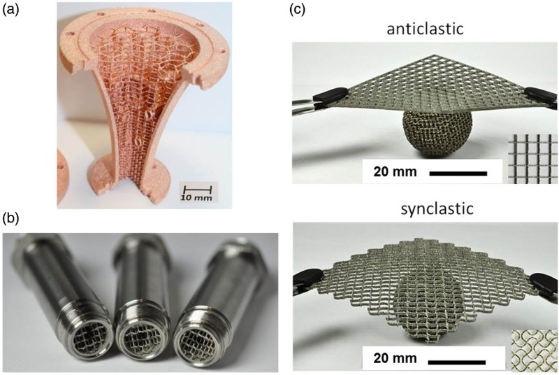
Metamaterials
The inherent design freedom of AM can also be exploited to produce cellular materials with unusual properties, so-called mechanical metamaterials. 98 The specific properties of metamaterials materialise by the design of the unit cell of the cellular structure. SEBM has been used to fabricate so-called auxetic materials which are characterised by a negative Poison’s ratio. 69,99 The response of auxetic materials to external mechanical loads is different from conventional materials, Fig. 12 c. Using mathematical optimisation methods, the properties of cellular materials can be further improved. 91 A systematic approach to identify cellular auxetic materials is described by Körner and Liebold-Ribeiro. 100
Besides the static mechanical properties, also the dynamic properties can be tailored by a specific design of the unit cell. Certain cell architectures develop full phononic band gaps where the propagation of elastic waves within a broad frequency band is completely suppressed. 93,101 Generally, cellular materials consisting of these rather complex unit cells are difficult to realise with conventional methods.
Summary and future prospects
AM, also denoted as 3D-printing, is believed to revolutionise future industrial production. Obvious advantages of AM are the reduction of development times, the production of small quantities or of individual items and last but not least, design freedom. Topologically optimised components can be fabricated, which can hardly or not be realised with conventional methods. The same is true for example for functional parts such as heat exchangers or medical implants.
SEBM belongs to the powder bed based class of AM technologies, where the powder is selectively molten with a high energy beam. It is very similar to SLM, but also different in important aspects. SEBM works under vacuum conditions which results in a better protection against contamination compared to SLM using argon as shielding gas. The main advantage of SEBM is the high power electron beam which can be moved at extremely high velocities and also be used for heating. This allows to apply innovative melting strategies and to work at very high temperatures. Due to stress-relief annealing, the level of residual stresses of SEBM parts is much lower than with SLM components. Thus, SEBM is especially suited for high-performance materials which are otherwise difficult of impossible to process.
Applying suitable processing parameters, the resulting SEBM materials properties are comparable to or better than that can be obtained by conventional production methods. In principle, the local materials properties can be adapted by adapting the local processing parameters. Furthermore, AM opens completely new possibilities to design novel classes of materials (architectured materials, metamaterials) with designed or novel properties and which cannot be realised with conventional processes.
The SEBM process is presently far from being completely developed. The potential of the electron beam is not even close to being fully exploited. This is true for the available beam quality (beam diameter is not constant but increases with increasing beam power), the beam power and also the overall process strategy. At the moment, one has just started to understand the process and to realise the potential of the electron beam. Future development must focus on a better process control in order to make higher beam powers with better beam quality usable. Up to now, alloys, which have been developed and optimised for forming or casting processes, are successfully used. Besides the development of enhanced SEBM machines, new materials and alloys for AM have to be designed in the future.
Footnotes
Acknowledgements
The author would like to acknowledge funding by the German Research Council (DFG) within the Cluster of Excellence ‘Engineering of Advanced Materials', the Collaborative Research Centre 814, project B2 and Collaborative Research Center TR 103, B2, at the University of Erlangen-Nuremberg. In addition, the author thanks the Bavarian State for the financial support in the framework of the technology transfer centre ‘VerTec’. The contributions in form of pictures and knowledge by the following members of the Department of Materials Science of the University Erlangen-Nuremberg and the Joint Institute of Advanced Materials and Processes in Fürth is acknowledged: A. Bauereiß, R. Guschlbauer, P. Heinl, H. Helmer, V. Jüchter, A. Klassen, Y. Liebold-Ribeiro, M. Lodes, M. Ramsperger, T. Scharowsky, J. Schwerdtfeger.