
Abstract
Amethod has been developed for fabricating polymer microstructures based on electric field induced self assembly and pattern formation. A dielectric fluid placed in between two conductive plates experience a force in an applied electric field gradient across the plates, which can induce a diffusive surface instability and self construction of the fluid surface. This process is exploited for the fabrication of self assembled polymer microstructures as well as replicated patterns through the use of pre-patterned plates or electrodes. FEM simulation is used to decide the minimum wavelength and electric gradient distribution of polymer structures. A variety of structures in the micron and nanometer scales including bio-fluidic MEMS, polymer optoelectronic devices can be fabricated using this method.
Introduction
Fabrication of structures in the micron and nanoscale via self assembly has attracted much interest in recent years. Self assembly methods range from fluidic self assembly of optoelectronic devices on silicon substrates (micron scale) to growing islands or quantum dots in heteroepitaxial film systems (nanoscale). These methods offer high throughput and low cost solutions compared to conventional patterning or lithography technologies, and they enable the fabrication of structures with dimensions beyond the wavelength of the light employed in most lithography processes. 1 –4
Self assembly of islands in heteroepitaxial films is based on the formation of a surface instability via surface diffusion at elevated temperatures in a growth reactor. 5 The driving for this process is the biaxial film stress induced by the lattice mismatch between the heteroepitaxial film and the substrate. The energy release rate per unit amplitude A of the surface features (islands or undulations) for this process is given by 6
where Y is called the surface admittance tensor and σ is the biaxial film stress. Surface roughening in heteroepitaxial films via surface diffusion has been studied extensively, and experimental results have shown that the surface evolution process takes place in the form of cycloids, two dimensional undulations and islands. 5 It has been shown theoretically that surface instability could also be induced by electrical loading in piezoelectric materials. The energy release rate for this process is described by, 7
where D is the electric field displacement vector, ε is the dielectric tensor and E is the applied electric field across a capacitor arrangement, as shown in Figure 1(a). Note that an air gap is necessary to provide a path for surface evolution. In this case, the piezoelectric material has a well defined crystallographic structure. It has been predicted that the level of electric fields required to induce cycloid formations on the surface are on the order of 1 GV/m. These theoretical predictions have led us to develop an idea to induce surface roughening as a way of patterning in polymer films (Figure 1(b)). The surface evolution process would require the polymer to be in a semi-liquid state to deform; and this is achieved by heating the polymer to its glass transition temperature (Tg). In this paper, we present this idea as a new self assembly technique for the fabrication of polymer structures based on electric field instability. The same principle can be extended to fabricate well defined and repeatable patterns by using prepatterned top electrode structures, as shown in Figure 1(c). This is termed as template replication.
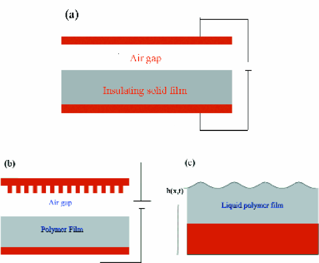
Capacitor arrangements to induce surface roughening in dielectric materials.
Materials and Methods
We have used silicon wafers and transparent ITO (Indium-Tin Oxide) coated quartz substrates to fabricate the capacitor structures. The bottom silicon plate is spin coated with a 100–200 nm thick polystyrene film. The polystyrene solution was prepared by dissolving polystyrene pellets in toluene, at a weight ratio of 11%. Spin coating at 4000 rpm for 30 seconds and subsequent hot plate drying (120C, 5 min) results in a film thickness of 200 nm. The ITO substrate was placed over the polymer surface at a distance to leave a thin air gap using spacers. This gap provides the necessary free space for surface evolution. The applied voltage to induce surface evolution in the polymer strongly depends on the thickness of the air gap. Theoretical predictions state that 10 GV/m is required to induce formations at the polymer surface. For a 100 nm thick air gap, this translates to an applied voltage of 100 V across the plates, and 1000 V for a 1 μm thick air gap. Several choices can be employed as spacers including micromachined spacers integrated in to the top plate or the bottom plate and photosensitive polymers with glass transition temperatures higher than that of polystyrene. In this study, patterned polymer spacers were used, in the thickness range of 100–1000 nm. For directed pattern transfer, ITO substrates were patterned by wet etching in (20% HCl + 5% HNO3) for 1–2 min. at 65C.

The bottom silicon plate had a heavily doped top layer, or n+ Si on the order of 5 microns for increased conductivity. The capacitor arangement was formed in a class-1000 clean room environment to minimize particle contamination. Ultra thin spacer and nanoscale patterning applications may require more stringent clean room conditions (class-10 or class-1). The whole assembly was mounted on a glass slide for handling purposes. An important part in building the capacitors is to form the electrical contacts for applying a bias voltage. For the bottom electrode/plate, a piece of conductive copper tape was applied right before spin coating the polymer (Figure 3A). For the top electrode, conductive copper tape was applied and the capacitor was formed with an offset configuration as shown in Figure 2. Wires are easily attached to the conductive tapes to connect to a voltage supply. The capacitor arrangement was placed over a hot plate and heated above the glass transition temperature of the polymer (Tg=170C). At the same time, the applied voltage was ramped using a constant voltage/current source. The capacitor arrangement was quenched intermittently by moving onto a steel plate and observations were made through the ITO/Quartz layer using an optical microscope.
Cross section of electric potential distribution.
Simulation Analysis
This simulation work thus explores the dynamical stability of dielectric liquid films between two electrically conducting counter-phases. It turns out that these films exhibit, quite generally, an instability driven by the electric field which builds up across the film due to the difference of the electronic work functions of the adjacent media. This leads to the amplification of the thermal surfaces waves and comprises strong mode selection. 8 The equation of motion for the lateral liquids flow in a thin film can be obtained from continuity equation
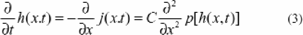
where C is the lateral coordinate, h(x. t) is the local film thickness, and j(x, t) is the lateral liquid flow in the film integrated along the normal coordinate. The shape of the flow profile and the viscosity of the liquid are absorbed into the positive constant C.
In general, a dielectric liquid film subjected to an electric field is unstable with respect to variations in surface shape, and the characteristic wavelength λ of the surface features is given by, 8
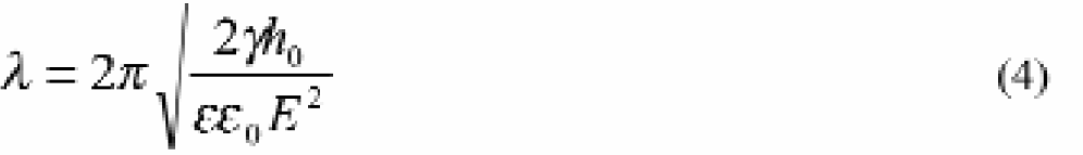
where γ is the polymer surface energy and h0 is the initial thickness of the polymer layer. This equation has been used to predict the size of the surface features as a function of the applied electric field in the self assembly process.
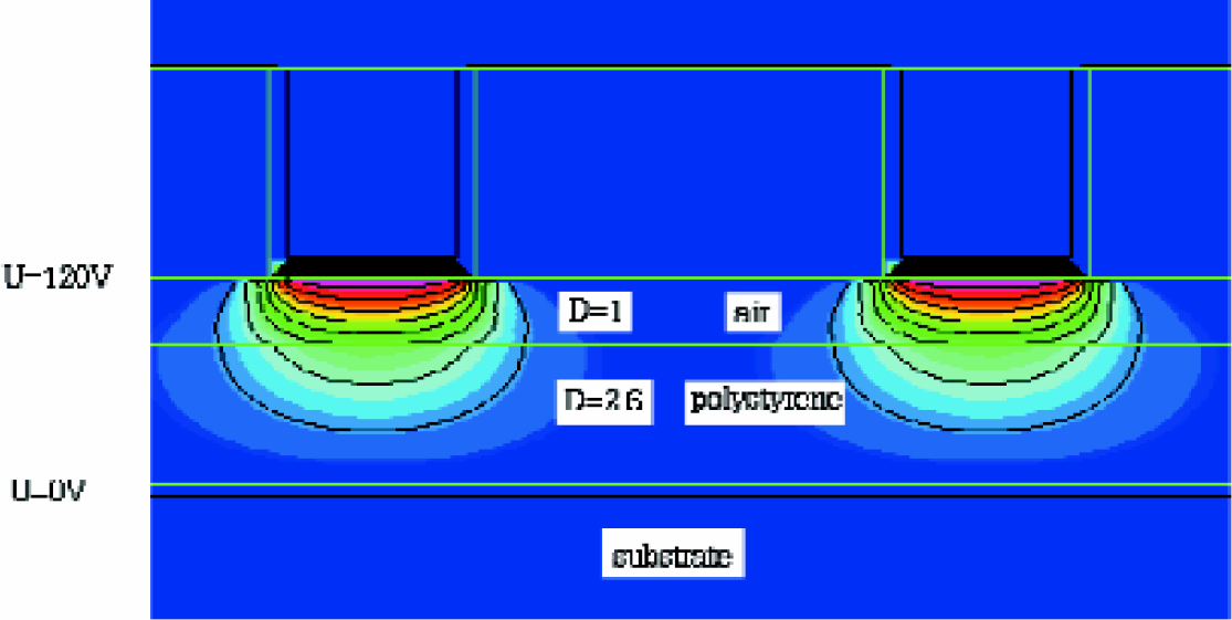
We have used CRDRC™, a multi-physics simulation software to analyze the self assembly process. Figure 3 shows a cross section of the electric field distribution for a 4×4 electrode array. Figure 4 is the minimum wavelength and the potential gradient on the polystyrene substrate.
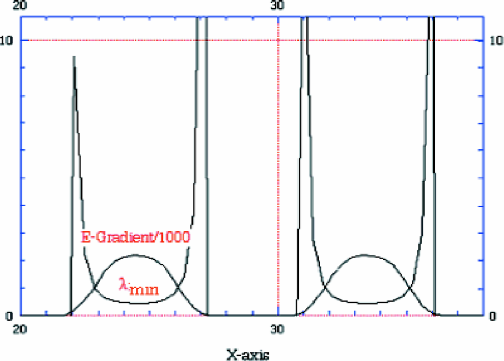
Minimum wavelength and the potential gradient on the polymer surface.
Results and Discussion
Figure 3 shows results from a self assembly experiment for which the initial polystyrene thickness was 200 nm and the spacer thickness was 400 nm. The capacitor arrangement was heated to 170C and a bias voltage of 120 V was applied across the capacitor. In Figure 5(a), heating was applied for 5 minutes, resulting in islands 2 microns in diameter.
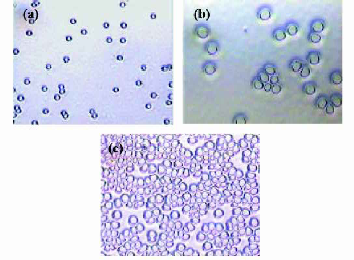
Self assembly of polystyrene structures at 170C and applied bias of 120 V.
After 20 minutes of annealing in Figure 5(b), the average island diameter is 5 microns. Locally close packed arrangement of features were also noted, in the form of a hexagonal arrangement as shown. After 40 minutes of annealing in Figure 5(c), the average island diameter is 18 microns. Additional experiments were conducted to measure the height of the islands using a dektak profiler. After 5 minutes and 40 minutes of annealing, the average height of islands is 345 nm and 375 nm, respectively. Throughout the experiments, a current flow of 100 nA-100 μA were noted through the capacitor arrangement, possibly due to ionic conduction through the polymer film. In general, both the lateral size of surface features and their height increase with annealing time. Further experiments have shown that, for a larger applied bias voltage, the size of the surface features are smaller, in accordance with the equation for characteristic wavelength (λ) given earlier. Similar work for polymer patterning has been cited in references 9 and 10 , for which the evolution or patterning times are on the order of hours, due to the lower applied bias voltages. Here we show that patterning can be accomplished in a time scale of minutes which is very practical in terms being a feasible technology for polymer microfabrication.
Figure 6 shows the results of two pattern replication experiments. For Figures 6(a)-(d), pre-patterned ITO/Quartz top plates were used, where the pattern was formed by conventional photolithography and wet etching. For both experiments, the bottom plate was n+ Si. For the experiment shown in Figures 6(a)-(b), the polystyrene film thickness was 200 nm and the spacer thickness was 600 nm. The capacitor arrangement was heated to 170 C, and a bias of 180 V was applied across the capacitor. The image shown in Figure 6(b) was obtained after 15 minutes of annealing. Dektak measurements have indicated that the features in the top mask were fully replicated on the polystyrene substrate. Average height of the features was 435 nm. In the second experiment (Figures 6(c) and 6(d)), the polystyrene film thickness was 200 nm and the spacer thickness was 500 nm. Again the capacitor setup was heated to 170°C and this time a bias voltage of 130 V was applied. After 5 minutes of anneal time, the setup was quenched to observe the partially completed line segment in Figure 6(c), which reveals undulations similar to that in the self assembly process. Complete formation was observed after 8 minutes of total processing time, as shown in Figure 6(d), and the average height measured was 410 nm. Note that the full spacer height was not obtained as the final feature height since this is a function of the annealing time. Other experiments with longer annealing times have shown that the height of the full gap can be achieved but the replicated polystyrene surface is poor after removal from the bottom plate due to adhesion. This will be addressed in future experiments through the use of proper surfactants as a molding release agent. The electric field instability process is a way of achieving self assembly and template replication in polymers. Reasonable fabrication times are possible by employing sufficiently high bias voltages. We believe that nanoscale fabrication is also very feasible, which will be very useful for many emerging applications in engineering and biology.
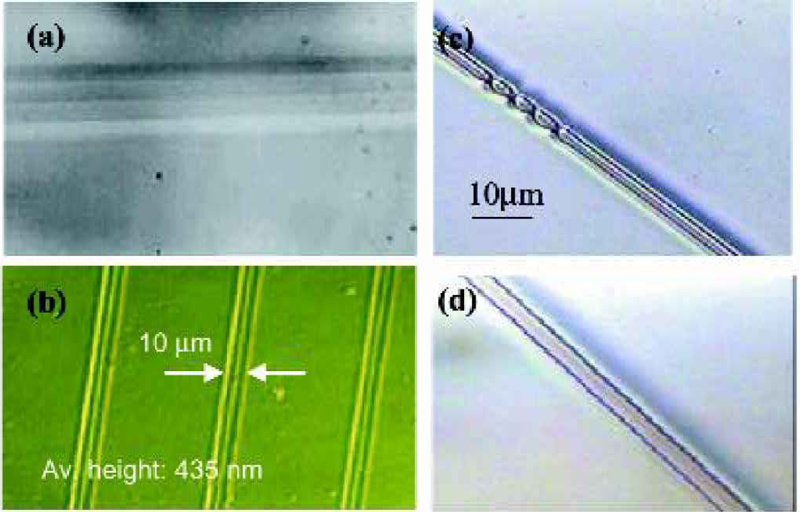
Results of pattern replication experiments in polymers.
Summary and Conclusion
A method has been described for self assembly and template replication in polymers. The method is based on a surface instability induced by an applied electric field. The process is useful for fabricating self assembled polymer microstructures as well as replicated patterns through the use of pre-patterned plates or electrodes. Potential applications of the method in the micron and nanometer scales include bio-fluidic MEMS, polymer optoelectronic devices and patterned templates for nanolithography.