
Abstract
Polymer microfabrication methods are becoming increasingly important as low-cost alternatives to the silicon or glass-based MEMS technologies. Polymer hot embossing and injection molding are replication methods applicable to microreplication of a diversity of materials and microstructures.
Equipment with high precision control of pressure and temperature for hot embossing of polymer materials is now available commercially. These systems have made possible the replication of chips containing microchannels for capillary electrophoresis (CE) and microfluidics devices, microoptical components and microreactors. Stable and reproducible polymer microstructures have been demonstrated in several types of materials with structural and optical properties meeting other biocompatibility and detection requirements. The process involves few variable parameters and results in high structural accuracy suited for a wide range of microfabrication applications.
After demonstrating equivalent and, in cases, improved performance, the alternative use of plastic as the microdevice material addresses needs for rapid prototyping in product development and provides cost advantages in product commercialization. Thus an increasing number of devices have been reported recently in the literature, fabricated on a variety of polymer substrates and using different fabrication methods such as laser ablation, injection molding, silicone rubber casting or embossing for microfabrication.
INTRODUCTION
Microsystems Technology (MST or MEMS) is now in its second decade of development. Some applications of microfabrication technology to bioanalytical systems conceptualized in the early 1990's 1 are now in early commercialization stage. The broad term “BioMEMS” encompasses a diverse number of applications related to molecular biology and the analysis of biological components. More scientifically, BioMEMS describes systems with micron dimensions and/or designed for applications in which the amounts of components involved get reduced to micro-dimensions or lower. For example, a microfluidic system for DNA analysis might be formed by an array of channels 10–50 micron in depth and width, which utilizes microliter volumes of samples for the separation and detection of DNA molecules in nanomolar or picomolar concentrations. In general terms, microarrays, microreactors and microfluidics are areas of BioMEMS being developed since the early 1990's addressing the need in molecular biology for large volume analysis of DNA, protein and other biomolecules. The terms do not exclude the analysis of other biological components for diagnostic applications or the analysis of large numbers of compounds generated through years of pharmaceutical product research. Furthermore, the terms also include the development of systems, which enhance the study of cells and microorganisms.
The use of plastics as structural materials for BioMEMS devices started to appear in scientific discussions and publications in 1994–96. 2,3 Given that plastics are main components in many biomedical devices, that field provides a large amount of data and knowledge supporting the two major reasons why plastic are very desirable materials in the microfabrication of devices in contact with biological systems. First, plastics offer a broad spectrum of adaptable fabrication technologies for product development and large-scale production. Second, given the large number of polymeric materials available based on the chemical and morphological composition, plastics offer a broad spectrum of physical and chemical properties available for the design of biocompatible systems. The range of possible mechanical properties, optical transmission and absorption and the possibilities for surface modification are valuable properties that plastics add to their use in biocompatible systems. The combination of properties and capacity of manufacturing makes plastics very suitable materials for the development of optimum cost-performance BioMEMS products. The broad range of technologies addressing issues related to the use of plastics in MEMS or MST research is identified as plastic microfabrication. 4
This paper summarizes the principles and applications of hot embossing as a technology in plastic microfabrication. Hot embossing plastic microfabrication starts from a single microfabricated master into the preparation of a tool and permits highly accurate replication on a diversity of thermoplastic materials for low and high volume production. The use of a single microfabrication step and the low cost of tooling make hot embossing a technology very suitable for low cost replication of development parts. Feasibility studies have demonstrated better and faster replication results with hot embossing when the devices involve high aspect ratio structures and high density of microcomponents.
HOT EMBOSSING PROCESS AND INSTRUMENTATION
Hot embossing is a form of polymer process related to the more macroscopic process of thermoforming, 5 in which a plastic sheet is manipulated as a rubbery solid or elastic liquid 6 under pressure. To reach the rubbery state the plastic sheet must be thermally equilibrated at a temperature above its glass transition (Tg) temperature. 7
The process of polymer microfabrication involves several steps, which are represented in Figure 1. From a concept or idea of micrometer size features, the design is translated into an electronic file of information prepared following the microfabrication guidelines of the technique to be used in the master generation step.
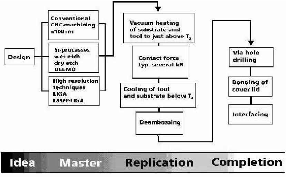
The preparation of a master is determined by the design itself (i.e., dimensions, geometrical parameters of microstructures, aspect ratios, etc.), and by the desired material to be used. Standard silicon wafers, glass, organic polymeric materials and metals have been used in the preparation of masters for hot embossing studies since the early developments of the technology.
After one master is prepared, it must be adapted to become a hot embossing tool. The steps involved in making a tool depend on the microfabrication material, the microfabricated features and the desired durability of the tool for the number of replication cycles. When the tool is fixed in a hot embossing system, the tool must contain the negative image of the desired features. Thus, in the embossing of a channel the tool will have defined ridges.
To initiate the replication stage of the polymer microfabrication chain, the tool is simply attached to the commercial system. With every combination of microfabrication tool and plastic material to use during replication, the experimentalist must tailor and optimize the embossing parameters for accurate and reproducible replication. The programming flexibility of the hot embossing systems allows this process to ocur in 1–2 hours depending on previous experience with the type of microstructures and the plastic material. For best results, plastic substrates should have a thickness of 0.5–2 mm. Vacuum controlled heating, followed by the application of compression force and rapid cooling are the basic elements defining an embossing cycle. After optimization, the replication of a number of parts is achieved by sequential embossing of plastic substrates with the optimized embossing process in cycles of 5–30 minutes of total processing time.
For the ultimate functionality of the microdevice, one or more completion steps may be involved depending on the level of integration.
MASTER MICROFABRICATION
In working with silicon microfabrication processes, it is possible to generate negative and positive microstructures by careful selection of the etching process. Standard wet etching and dry etching techniques are possible 8 for silicon and glass. Beyond standard considerations about design and microstructure dimensions, it is also very important to design the master microfabrication process to provide smooth surface to the final microfabricated features. The logic behind this is the critical role that surface roughness plays in the demolding of the plastic microreplicated part after the completion of the embossing process. Even submicron undercut structures make the process of demolding detrimental to the plastic part or the tool, depending on the forces involved. This is a general consideration for all plastic microfabrication with the exception of work done in elastomeric materials. Elastomeric materials have elastic memory that permits higher levels of surface structure in the microfabricated master due to the possible deformation and recovery that might occur during and after demolding. The considerations of master microfabrication and surface roughness become of utmost importance when the microstructures must have high aspect ratios. 9
The LIGA and Laser-LIGA processes work with organic polymeric materials. In either technique, the generated microstructures correspond to the positive features of the desired plastic microparts. Galvanoforming or electroforming processes can be used to translate a plastic microfabricated master into a metal tool (electroform) to be used in the hot embossing system. Nickel and Nickel-Chromium electroforms are typical for the process.
The use of CNC micromachining is also possible for dimensional structures down to 100 micron in metal substrates. The combination of standard microfabrication and CNC micromachining can be also effective in producing the final tool to build more macroscopic features connecting the microstructures.
Silicon masters are too fragile for typical hot embossing pressures and need some form of reinforcement for the durability of the master for the intended number of replication cycles. Most typically, silicon wafers are reinforced by anodic bonding to glass wafers. This approach is available at most microfabrication centers and MEMS foundries, and provides the sorter cycle time to a hot embossing tool. The tradeoff of using this type of tool is the durability of the tool and the number of possible replication cycles. For greater tool durability and replication performance, the preparation of a metal tool using standard galvanic processes is also recommended. The preparation of electroform replicas of the microfabricated master requires the use of a conductive layer and involves significantly more time for completion.
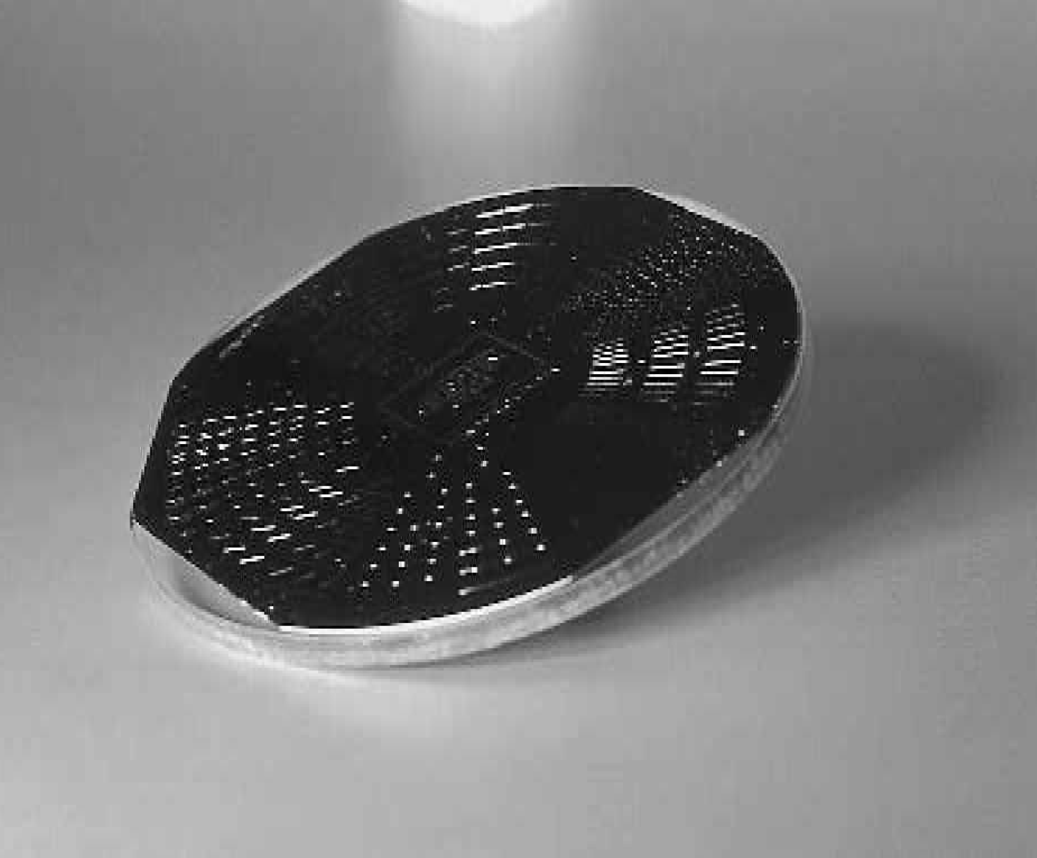
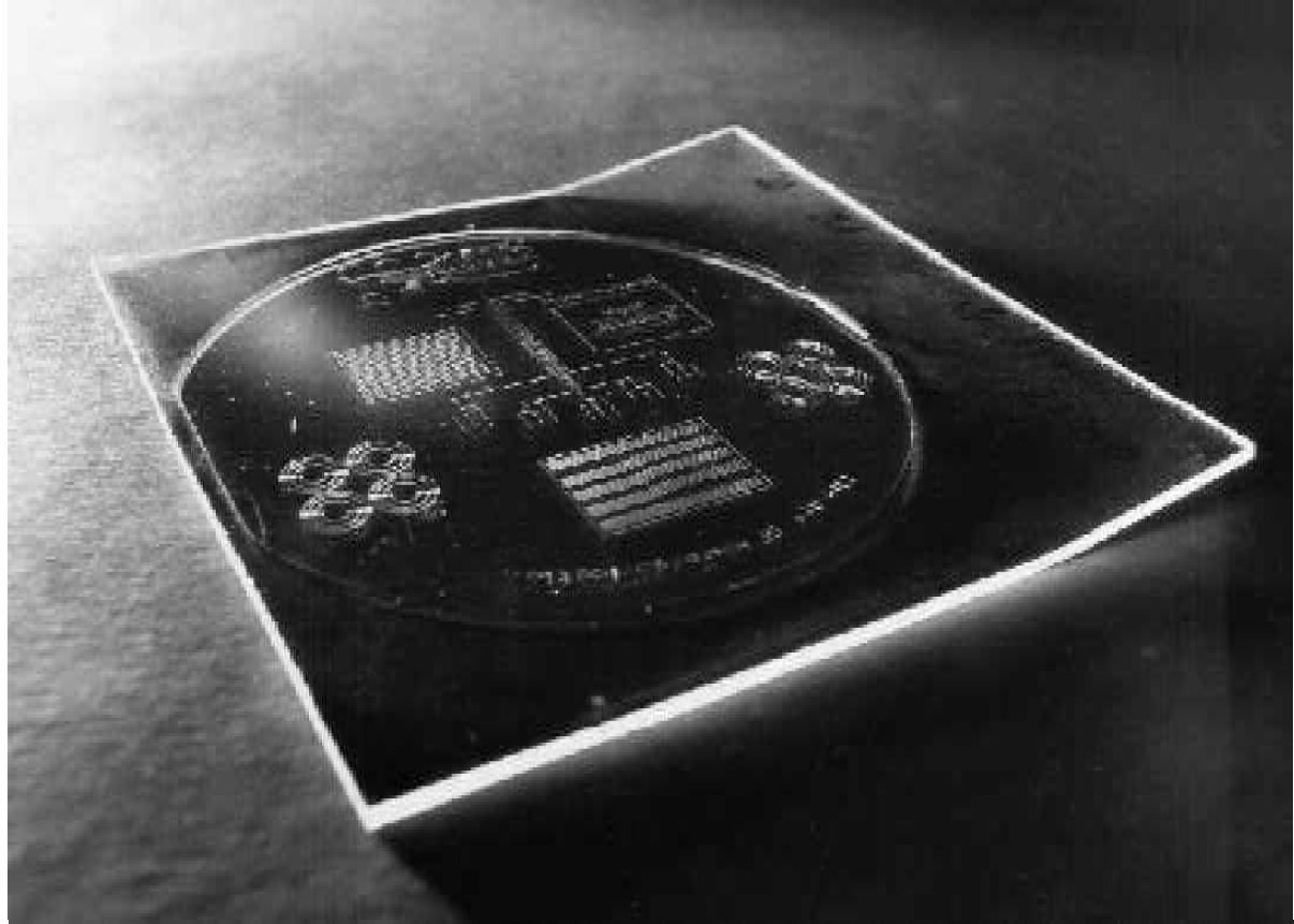
The reader is directed to the literature for more details in all aspects of microfabrication. Figure 2 provides the image of a testing silicon master anodically bonded to a glass wafer. In this case the glass wafer is 5 mm thick and has the exact same diameter as the silicon wafer. The diced areas of the silicon wafer are designed for the fitting of the tool to a tool-holder accessory of a hot embossing system.
PLASTIC CONSIDERATIONS
Hot embossing works with a preformed sheet of thermoplastic or slightly crosslinked plastic material. Plastic sheets of different thickness are available from different manufacturers and distributors of polymeric materials. Flats of customized thickness can be generated using standard injection molding techniques such as resins.
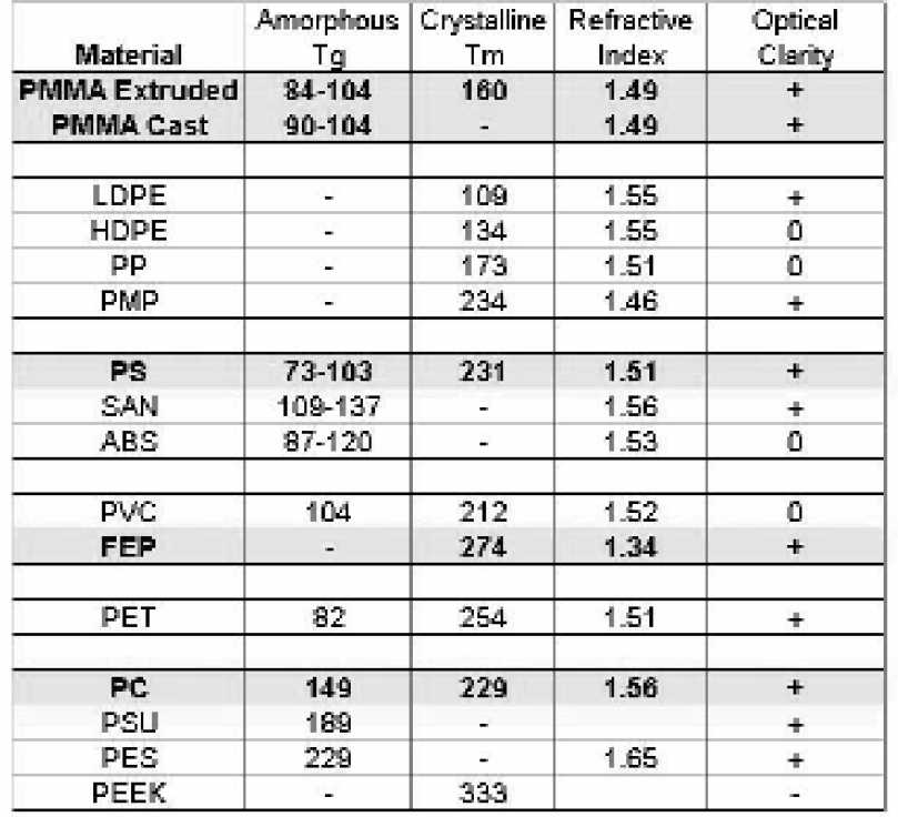
The selection of a plastic substrate for hot embossing must be determined by the performance requirements of the plastic micropart. Optical clarity, optical absorption and transmission at operating frequencies, surface properties and biocompatibility are the most common parameters to use in the selection of plastics for hot embossing. Morphological properties of plastic material such as the level of crystallinity, stress and orientation are also relevant to the optimization of the hot embossing parameters. Amorphous materials such as polymethylmethacrylate (PMMA) behave ideally for most hot embossing replication. In working with partially crystalline materials, the experimentalist has to understand that these will exhibit a second transition between the rubbery state and the melt state. This is a primary type of transition around which slow melting and recrystallization processes of the polymeric material can occur that might result in changes in the final properties of the plastic.
The highly accurate replication results of hot embossing derive from the capacity to work at temperatures right above the Tg. This minimizes the build up of stress and reduces changes in the physical properties of the material. The Table in Figure 3 summarizes glass transition (Tg) and melting temperatures (Tm) for very typical thermoplastic materials. Highlighted materials PMMA, polycarbonate (PC), polystyrene (PS) and fluorinated thermoplastic (FEP) are the most desirable materials for hot embossing of BioMEMS and microoptical components. These materials offer high optical clarity and have a long history as biomedical materials. With most plastics, embossing temperatures of 10–30 degrees above the Tg are sufficient to reach the rubbery state and allow for hot embossing of microfabricated features with practically no stress added during the imprinting process. Other thermoplastic materials listed in Figure 3 are being considered for hot embossing plastic microfabrication due to the interest in development of microdevices offering higher operating temperatures, or chemical resistance or enhanced optical properties. Since in many applications, the polymeric material forms the window to detection, it is important to understand the potential changes in refractive index with different plastics. The absence or presence of additives in the preformed plastic sheet also has to be considered for optimum results.
HOT EMBOSSING PRINCIPLES AND HARDWARE
Hot embossing microreplication is based on the imprinting of microstructures onto a preformed plastic sheet in specially designed presses. The process relies in the careful control of temperatures and pressures needed during the process. Commercially available systems made by Jenoptik Mikrotechnik GmbH for hot embossing are designed with electrically heated plates with embedded coils for re-circulation of special oils used as cooling fluid. These heating plates are fitted to a force frame, which permits the application of up to 250 KN of force over the entire embossed surface. In most configurations, the tool-holder with the microfabrication tool is attached to the upper plate, while the plastic substrate is attached to the lower plate of the force frame. The embossing process takes place in an enclosed chamber designed to maintain down to 0.1 mbar of vacuum pressure. Careful alignment of the plate's planarity and demolding tools added to the careful control of heating rates and times permit the replication quality of microreplication shown in several studies and publications referenced in this publication. A few selective examples of embossing results are given below. The standard equipment for hot embossing has a maximum embossing area of 15×15 cm 2 . Equipment for larger embossing areas is under development.
There are three basic steps in hot embossing. The first step corresponds to the thermal equilibration of the tool and the plastic substrate to a temperature above Tg. For most applications the tool and the substrate are equilibrated to the same temperature, but it is possible to independently control each hot plate to attain optimum replication results. In the second step, the tool is compressed against the substrate to a predesigned maximum force or predefined penetration depth. Ultimate embossing pressures are of the order of several KN/cm 2 . In step three, the already microfabricated part is cooled very rapidly to a temperature below the Tg. Upon reaching thermal equilibration below Tg, the plastic material transitions back to the glassy rigid state providing stable microstructures imprinted on the surface of the plastic substrate. After this step, the part is separated from the tool using demolding elements.
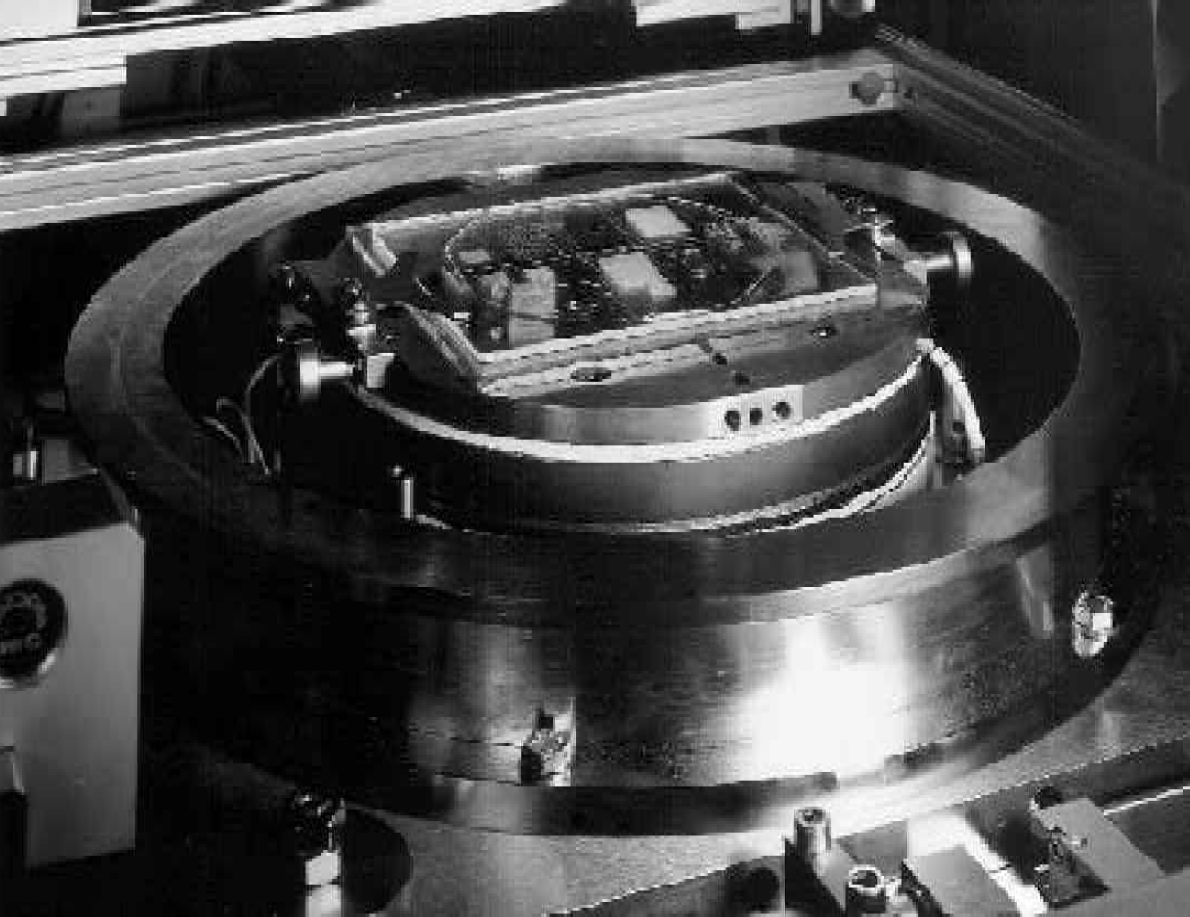
For best deembossing results, the microfabrication tool has to have appropriate surface structure and poor adhesion between the tool and the thermoplastic material. The use of mold release agents facilitates deembossing if possible mold release transferred to the microparts during embossing is compatible with the intended functionality. With most typical materials, the systems permit the optimization of hot embossing cycles of 5–20 minutes per part. Figure 4 is an image of an open hot embossing chamber after completion of the embossing cycle, showing how a micropart remains attached to the lower plate. Figure 5 shows a micropart with several typical microfabricated structures on a PMMA substrate. This micropart is now ready for use or for back end processing depending on the intended application.
BACK-END INTEGRATION
The last step in the plastic microfabrication chain is described in a general way as back-end integration because it encompasses several possible technologies that make possible the ultimate functionality of a micropart and/or the addition of functional elements to the final microdevice. For example in microfluidics, the formation of channels requires the addition of a cover layer that defines the fourth wall delimiting the channel. Several bonding technologies to join similar and dissimilar plastics have been described and proposed in the literature. The challenge of bonding microstructures is set by the dimensions of the surface to build the bonding interfaces and the control of the surface energy that dominates in the structures due to the large surface to volume ratio. For most microfluidic applications, the final devices do not require high bonding strengths provide uniform and tight enclosure of the channels to avoid liquid migration to the interface by capillary action during the utilization of the devices.
As the microparts and microdevices gain complexity and functional capacity, other processes are being added to the total process of plastic microfabrication. Examples include the drilling of holes to access the microstructures from the macroscopic world of sample and reagent addition. Also possible is the metallization of electrical contacts in microdimensions for devices using electric fields or electrochemical sensors. Other back-end processes might involve the addition of reagents and subsequent processing steps for stabilization of reagents during storage. The integration of optical elements for optical detection, the integration of electronic components, the addition of elements in the z-dimension for connectivity to the environment, macroscopic packaging and labeling for device identification and tracking of data.
RESULTS AND APPLICATIONS
Several publications from the technical literature and conference proceedings describe detailed design and experimentation in several plastic microfabrication systems.
MICROREACTORS
Microreactors are defined broadly as microstructures suitable to carry out parallel reactions. This concept could be applied to the area of combinatorial generation of substances and compounds or to the area of micrototal analysis systems (μTAS). 10 In μTAS concepts, the only step carried out outside the microdevice environment is the addition of sample and reagents. Other necessary steps for total analysis might involve analyte isolation, concentration, dilution, amplification, labeling, or incubation. These are all steps that in all cases require some sort of physical interaction or chemical/biochemical reaction. Typical examples of these are the isolation of DNA material from physiological fluids, the amplification of DNA samples using micro PCR, and mixing of fluids and reagents for fluorescence labeling.
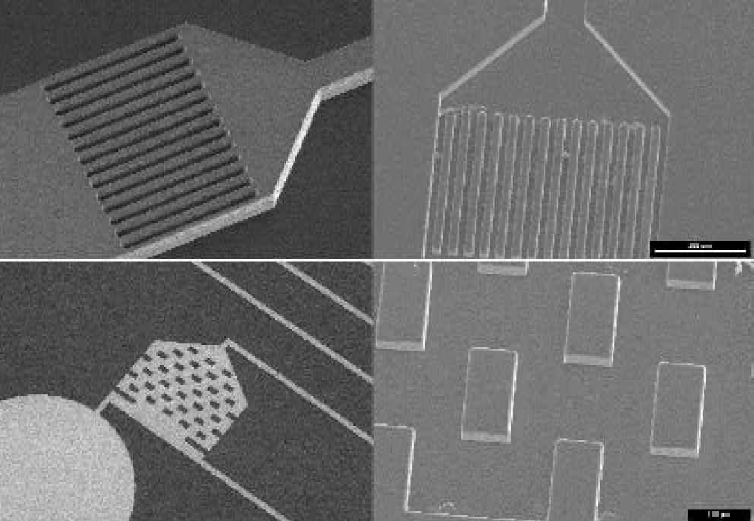
Examples of microstructures designed for these purposes are illustrated in Figure 6. 11 At the left-hand side of Figure 6, SEM images of silicon tools prepared using an advanced DRIE process. The two images on the right hand side of Figure 6 correspond to SEM images taken from hot embossed microparts replicated in PMMA. The upper two images in Figure 6 correspond to a filtration device designed for the separation of cells and particles of different sizes. The lower two images in Figure 6 correspond to the design of mixing elements in a microfluidic layout of channels. In the later case blocks, of 1×1.5 μm 2 were added to a larger cavity area to disrupt the laminar flow typicallyoccurring in microfluidic systems.
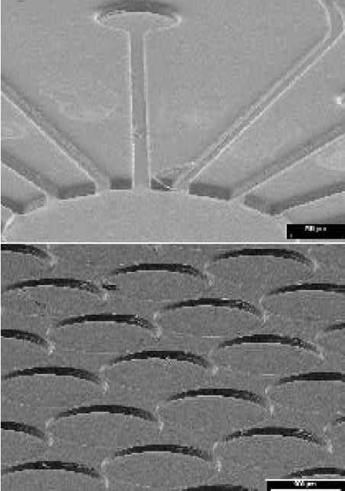
Other examples and structures had been replicated in polycarbonate and polyolefin plastic materials for PCR applications and for single cell analysis work. Figure 7 corresponds to PC embossed structures of an array of microcavities designed for cellular isolation, with microfluidic structures connected to some of the micro-cavities for fluid handling during analysis.
MICROFLUIDICS
Microfluidic systems are intended for the handling of fluids in microdimensional channels and structures. Applications of plastic microfabrication in this field evolved mostly from the adaptation of electrophoretic separations in microcapillary channels built in planar structures. The field evolved from the field of capillary electrophoresis (CE) which was earlier developed using fused silica capillaries. Microfluidic systems controlled by electric fields work with electrophoretic and electroosmotic effects to manage fluid distribution and molecular separation. The use of pneumatic fluid control is also possible with the integration of microvalves, micropumps and more sophisticated microchannel structures. Although initial work in this area was limited to glass microchips, the interest and research directed toward the use of plastics is spreading very fast.
Electrophoresis and electroosmotic flow are phenomena that depend on the presence of electrical charges that can be oriented and controlled in the presence of electric fields. In electrophoretic movement, the mass and charge of individual species define the rate and direction of displacement of individual molecules and this makes it possible to sort or separate based on electrophoretic mobility. Crosslinked and entangled polymer gels can also be used in these systems for the separation of biomolecules based on size. For the electroosmotic effects to take place, the charges must be localized in the surface of the microchannel. Thus when plastics are considered for the replacement of glass in microchip structures, the selection of the material plays a major role in controlling the desired density charges on the surface or from the application of surface modification techniques intended to build surface charges on the walls defining the channels.
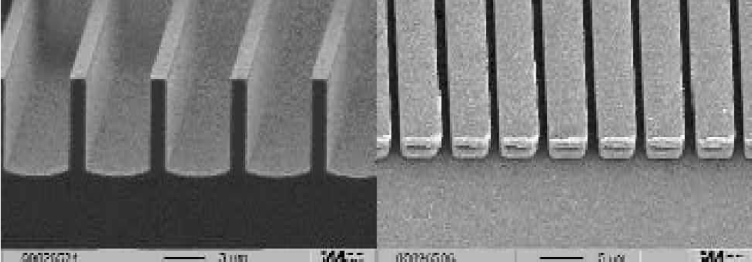
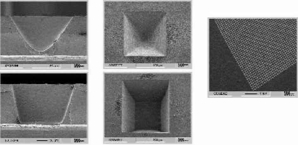
Typical microfluidic structures are formed from the crossing of channels with dimensions in the range of 10–100 μm. 11 These crossecting channels are effectively used under controlled mechanical or electrical fields to measure and dispense nanoliter or picoliter volumes of sample from one channel into the intercepting channel. Plastic microfabricated structures for microfluidics include the wet and dry etching process for master fabrication and a diversity of geometrical distribution of channels to provide channel density for packing of microstructures and channel length needed for separation capacity. Of the numerous types of structures prepared by hot embossing for microfluidic applications, Figure 8 provides the SEM images of the silicon master and the corresponding PMMA replicated micropart. In this example, an array of parallel channels, 1 μm wide and 5 μm high, was replicated in PMMA from a master prepared by a DRIE process on silicon wafers. Replication results are shown in the right hand side of Figure 8; the quality of the silicon master is observed on the left-hand side. This example is characteristic of a replication of high aspect ratio (about 5/1) structures and the replication of highly orthogonal walls with the capacity for packing several structures in very small surface areas.
MICROARRAYS
Plastic microfabrication fits in the now well-developed field of microarrays in two different ways: As microfluidic components to DNA arrays and as substrate structures for proteomics applications. The first has been extensively explored, 13 but proteomics applications are more at the research stage. The capacity for surface modification of plastics plays a major role in proteomic applications.
A second form of microarrays in which hot embossing has shown an advantage over more classical injection molding techniques is in the microfabrication of high density arrays of wells 100–300 micron in diameter for nanoliter volume chemistry. Figure 9 provides SEM images of nanowell crossections and top geometry in a process initiated with the microfabrication of a master using UV-LIGA ablation of PMMA coated over a titanium wafer. 14,15 In the study by Becker and Klotzbücher 10 , the careful selection of the Excimer ablation parameters permitted the generation of very smooth microfabricated surfaces defining the wells. Furthermore, it permitted the control of the slope of the wall at 45–90 degrees for the nanowell as a means to affect the dispensing of liquids and microparticles into the nanowells for the intended functionality of these microarrays. Using this type of geometry, it is possible to build arrays of 100–300 thousand nanowells in standard microtiter plate areas 10 as shown in the furthest right-hand image of Figure 9.
FUTURE DEVELOPMENTS
Having demonstrated hot embossing as an accurate and cost effective polymer microfabrication technology, the next challenge comes in the automation of the replication and back-end integration process toward the fabrication of large volumes of microparts or microdevices ready for delivery to the application lab. We are working toward this objective with the goal of having a pilot line ready for volume production in the first half of the year 2001. This process involves the adaptation and development of robotic systems capable of locating, transporting and allocating microfabricated parts with an accuracy of 10–20 microns. On-going results from the implementation and validation of the pilot line will be presented in future publications and scientific presentations.
ACKNOWLEDGEMENT
The author wishes to express her acknowledgement to the Jenoptik Mikrotechnik team of engineers and scientists. With special acknowledgement to Wolfram Dietz, Ulf Heim, and Oliver Rötting for their experimental contributions to the hot embossing studies. To the continuous support of collaborators and customers always willing to explore the possibilities that the technology offers.
GORE TTY ALONSO-AMIGO
In her function of Head of US Operations for Mildendo GmbH, Dr. Alonso is responsible for marketing plastic microfab-rication technology to companies in the areas of BioMEMS and microoptical communication.
She is a native of Spain, and came to the US for graduate studies. She has a Ph.D., in Polymer Chemistry from University of Detroit-Merci (1988) and a Master in Business (MSTM) from Pepperdine University (1999). She has twelve years of experience in medical devices and microfluidics.